


OP184EP
Table of contents
 Loading...
Analog Devices OP184EP, OP184FS, OP284FP, OP484FP, OP484ES Datasheet
...
Precision Rail-to-Rail Input & Output
1
2
3
45
6
7
8
OUT A
–IN A
+IN A
V–
OP-482
V+
OUT B
–IN B
+IN B
OP284
a
FEATURES
Single-Supply Operation
Wide Bandwidth: 4 MHz
Low Offset Voltage: 65 mV
Unity-Gain Stable
High Slew Rate: 4.0 V/ms
Low Noise: 3.9 nV/√
APPLICATIONS
Battery Powered Instrumentation
Power Supply Control and Protection
Telecom
DAC Output Amplifier
ADC Input Buffer
GENERAL DESCRIPTION
The OP184/OP184/OP284/OP484 are single, dual and quad
single-supply, 4 MHz bandwidth amplifiers featuring rail-to-rail
inputs and outputs. They are guaranteed to operate from +3 to
+36 (or ±1.5 to ±18) volts and will function with a single supply
as low as +1.5 volts.
These amplifiers are superb for single supply applications requiring both ac and precision dc performance. The combination
of bandwidth, low noise and precision makes the OP184/OP284/
OP484 useful in a wide variety of applications, including filters
and instrumentation.
Other applications for these amplifiers include portable telecom
equipment, power supply control and protection, and as amplifiers or buffers for transducers with wide output ranges. Sensors
requiring a rail-to-rail input amplifier include Hall effect, piezo
electric, and resistive transducers.
The ability to swing rail-to-rail at both the input and output enables designers to build multistage filters in single-supply systems and maintain high signal-to-noise ratios.
The OP184/OP284/OP484 are specified over the HOT extended
industrial (–40°C to +125°C) temperature range. The single
and dual are available in 8-pin plastic DIP plus SO surface
mount packages. The quad OP484 is available in 14-pin plastic
DIPs and 14-lead narrow-body SO packages.
Hz
Operational Amplifiers
OP184/OP284/OP484
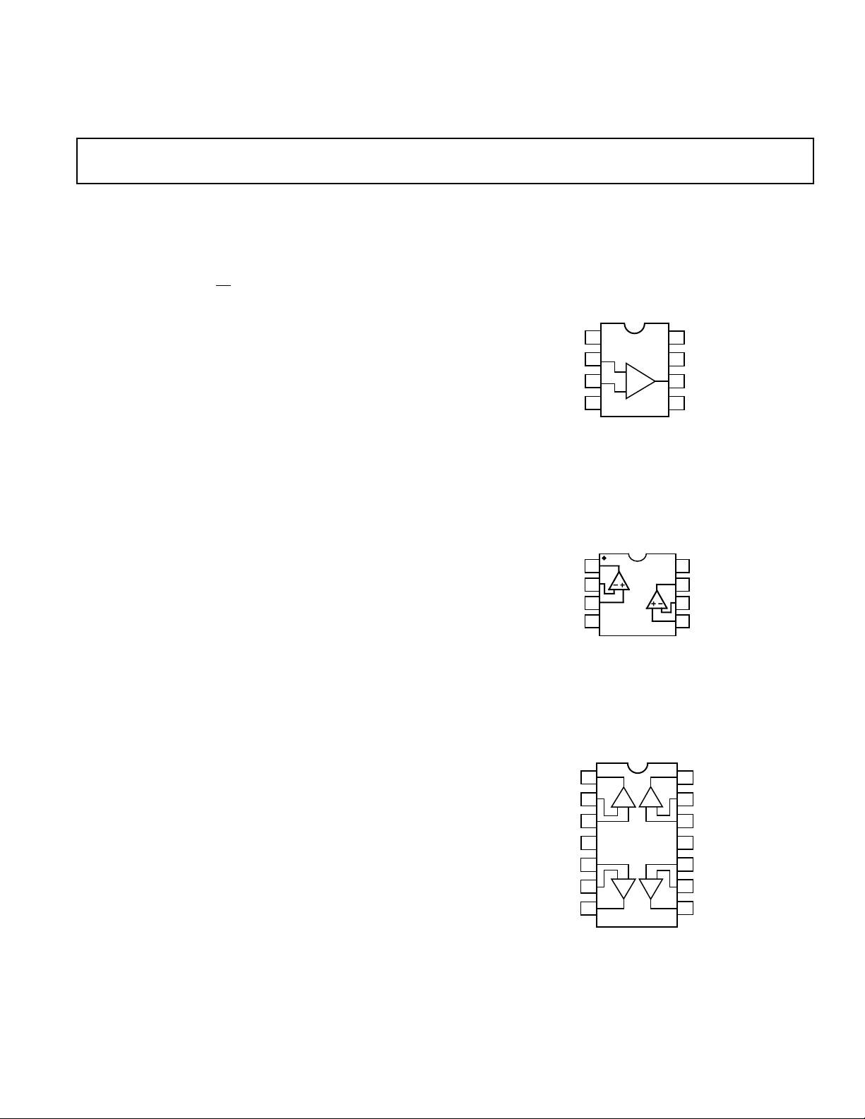
PIN CONFIGURATIONS
8-Lead Epoxy DIP
(P Suffix)
8-Lead SO
(S Suffix)
NULL
1
OP184
2
–IN A
+IN A
V–
–
3
+
4
NC = NO CONNECT
8-Lead Epoxy DIP
(P Suffix)
8-Lead SO
(S Suffix)
14-Lead Epoxy DIP
(P Suffix)
14-Lead Narrow-Body SO
(S Suffix)
OUT A
1
2
–IN A
+IN A
V+
+IN B
–IN B
OUT B
–+
3
4
OP484
5
–+
6
7
NC
8
V+
7
OUT A
6
NULL
5
OUT D
14
13
–
–+
–IN D
12
+IN D
11
V–
+IN C
10
–IN C
9
8
OUT C
+
REV. 0
Information furnished by Analog Devices is believed to be accurate and
reliable. However, no responsibility is assumed by Analog Devices for its
use, nor for any infringements of patents or other rights of third parties
which may result from its use. No license is granted by implication or
otherwise under any patent or patent rights of Analog Devices.
© Analog Devices, Inc., 1996
One Technology Way, P.O. Box 9106, Norwood. MA 02062-9106, U.S.A.
Tel: 617/329-4700 Fax: 617/326-8703

OP184/OP284/OP484–SPECIFICA TIONS
ELECTRICAL CHARACTERISTICS
(@ VS = +5.0 V, VCM = 2.5 V, TA = +258C unless otherwise noted)
Parameter Symbol Conditions Min Typ Max Units
INPUT CHARACTERISTICS
Offset Voltage “OP184/284E” Grade V
Offset Voltage “OP184/284F” Grade V
Offset Voltage OP184 “484E” Grade V
Offset Voltage OP184 “484F” Grade V
Input Bias Current I
Input Offset Current I
OS
OS
OS
OS
B
OS
(Note 1) 65 µV
–40°C ≤ T
≤ +125°C 165 µV
A
125 µV
–40°C ≤ T
≤ +125°C 350 µV
A
75 µV
–40°C ≤ T
≤ +125°C 175 µV
A
150 µV
–40°C ≤ T
≤ +125°C 450 µV
A
60 300 nA
–40°C ≤ T
≤ +125°C 500 nA
A
250nA
–40°C ≤ T
≤ +125°C50nA
A
Input Voltage Range 0+5V
Common-Mode Rejection Ratio CMRR V
Common-Mode Rejection Ratio CMRR V
Large Signal Voltage Gain A
VO
= 0 V to 5 V 60 dB
CM
= 1.0 V to 4.0 V, –40°C ≤ TA ≤ +125°C86 dB
CM
RL = 2 kΩ, 1 V ≤ VO ≤ 4 V 50 240 V/mV
R
= 2 kΩ, –40°C ≤ TA ≤ +125°C 25 V/mV
L
Bias Current Drift ∆IB/∆T 150 pA/°C
OUTPUT CHARACTERISTICS
Output Voltage High V
Output Voltage Low V
Output Currrent I
OH
OL
OUT
IL = 1.0 mA +4.85 V
IL = 1.0 mA 125 mV
± 6.5 mA
POWER SUPPLY
Power Supply Rejection Ratio PSRR V
Supply Current/Amplifier I
Supply Voltage Range V
SY
S
= +2.0 V to +10 V, –40°C ≤ TA ≤ +125°C76 dB
S
VO = 2.5 V, –40°C ≤ TA ≤ +125°C 1.25 mA
+3 +36 V
DYNAMIC PERFORMANCE
Slew Rate SR R
Settling Time t
s
= 2 kΩ 1.65 2.4 V/µs
L
To 0.01%, 1.0 V Step 2.5 µs
Gain Bandwidth Product GBP 3.25 MHz
Phase Margin Øo 45 Degrees
NOISE PERFORMANCE
Voltage Noise e
Voltage Noise Density e
Current Noise Density i
NOTES
1
Input Offset Voltage measurements are performed by automated test equipment approximately 0.5 seconds after application of power.
Specifications subject to change without notice.
p-p 0.1 Hz to 10 Hz 0.3 µV p-p
n
n
n
f = 1 kHz 3.9 nV/√Hz
0.4 pA/√Hz
–2–
REV. 0

OP184/OP284/OP484
ELECTRICAL CHARACTERISTICS
(@ VS = +3.0 V, VCM = 1.5 V, TA = +258C unless otherwise noted)
Parameter Symbol Conditions Min Typ Max Units
INPUT CHARACTERISTICS
Offset Voltage “OP184/284E” Grade V
Offset Voltage “OP184/284F” Grade V
Offset Voltage OP184“484E” Grade V
Offset Voltage OP184“484F” Grade V
Input Bias Current I
Input Offset Current I
OS
OS
OS
OS
B
OS
(Note 1) 65 µV
–40°C ≤ T
≤ +125°C 165 µV
A
125 µV
–40°C ≤ T
≤ +125°C 350 µV
A
100 µV
–40°C ≤ T
≤ +125°C 200 µV
A
150 µV
–40°C ≤ T
≤ +125°C 450 µV
A
60 300 nA
–40°C ≤ T
≤ +125°C 500 nA
A
–40°C ≤ TA ≤ +125°C50nA
Input Voltage Range 0+3V
Common-Mode Rejection Ratio CMRR V
= 0 V to 3 V 60 dB
CM
Common-Mode Rejection Ratio CMRR VCM = 0 V to 3 V, –40°C ≤ TA ≤ +125°C56 dB
OUTPUT CHARACTERISTICS
Output Voltage High V
Output Voltage Low V
OH
OL
IL = 1.0 mA +2.85 V
IL = 1.0 mA 125 mV
POWER SUPPLY
Power Supply Rejection Ratio PSRR V
Supply Current/Amplifier I
SY
= ±1.25 V to ±1.75 V 76 dB
S
VO = 1.5 V, –40°C ≤ TA ≤ +125°C 1.15 mA
DYNAMIC PERFORMANCE
Gain Bandwidth Product GBP 3 MHz
NOISE PERFORMANCE
Voltage Noise Density e
NOTES
1
Input Offset Voltage measurements are performed by automated test equipment approximately 0.5 seconds after application of power.
Specifications subject to change without notice.
n
f = 1 kHz 3.9 nV/√Hz
REV. 0
–3–
OP184/OP284/OP484
ELECTRICAL CHARACTERISTICS
(@ VS = 615.0 V, VCM = 0 V, TA = +258C unless otherwise noted)
Parameter Symbol Conditions Min Typ Max Units
INPUT CHARACTERISTICS
Offset Voltage “OP184/284E” Grade V
Offset Voltage “284F” Grade V
Offset Voltage “484E” Grade V
Offset Voltage “484F” Grade V
Input Bias Current I
Input Offset Current I
OS
OS
OS
OS
B
OS
(Note 1) 100 µV
–40°C ≤ T
≤ +125°C 200 µV
A
175 µV
–40°C ≤ T
≤ +125°C 375 µV
A
150 µV
–40°C ≤ T
≤ +125°C 300 µV
A
250 µV
–40°C ≤ T
≤ +125°C 500 µV
A
80 300 nA
–40°C ≤ T
≤ +125°C 500 nA
A
–40°C ≤ TA ≤ +125°C50nA
Input Voltage Range –15 +15 V
Common-Mode Rejection Ratio CMRR V
Common-Mode Rejection Ratio CMRR V
Large Signal Voltage Gain A
Offset Voltage Drift “E” Grade ∆ V
VO
/∆T 0.2 2.00 µV/°C
OS
= –14.0 V to +14.0 V, –40°C ≤ TA ≤ +125°C86 90 dB
CM
= –15.0 V to +15.0 V 80 dB
CM
RL = 2 kΩ, –10 V ≤ VO ≤ 10 V 150 1000 V/mV
= 2 kΩ, –40°C ≤ TA ≤ +125°C 75 V/mV
R
L
Bias Current Drift ∆IB/∆T 150 pA/°C
OUTPUT CHARACTERISTICS
Output Voltage High V
Output Voltage Low V
Output Current I
OH
OL
OUT
IL = 1.0 mA +14.8 V
IL = 1.0 mA –14.875 V
±10 mA
POWER SUPPLY
Power Supply Rejection Ratio PSRR V
Supply Current/Amplifier I
Supply Current/Amplifier I
SY
SY
= ±2.0 V to ±18 V, –40°C ≤ TA ≤ +125°C90 dB
S
VO = 0 V, –40°C ≤ TA ≤ +125°C 1.75 mA
VS = ± 18 V, –40°C ≤ TA ≤ +125°C 2.0 mA
DYNAMIC PERFORMANCE
Slew Rate SR R
Full-Power Bandwidth BW
Settling Time t
p
S
= 2 kΩ 2.4 4.0 V/µs
L
1% Distortion, RL = 2 kΩ, VO = 29 V p-p 35 kHz
To 0.01%, 10 V Step 4 µs
Gain Bandwidth Product GBP 4.25 MHz
Phase Margin Øo 50 Degrees
NOISE PERFORMANCE
Voltage Noise e
Voltage Noise Density e
Current Noise Density i
NOTES
1
Input Offset Voltage measurements are performed by automated test equipment approximately 0.5 seconds after application of power.
Specifications subject to change without notice.
p-p 0.1 Hz to 10 Hz 0.3 µV p-p
n
n
n
f = 1 kHz 3.9 nV/√Hz
0.4 pA/√Hz
W AFER TEST LIMITS
(@ VS = +5.0 V, VCM = 2.5 V, TA = +258C unless otherwise noted)
Parameter Symbol Conditions Limit Units
Offset Voltage OP284 V
Offset Voltage OP484 V
Input Bias Current I
Input Offset Current I
Input Voltage Range V
Common-Mode Rejection Ratio CMRR V
Power Supply Rejection Ratio PSRR V
Large Signal Voltage Gain A
Output Voltage High V
Output Voltage Low V
Supply Current/Amplifier I
NOTE
Electrical tests and wafer probe to the limits shown. Due to variations in assembly methods and normal yield loss, yield after packaging is not guaranteed for standard
product dice. Consult factory to negotiate specifications based on dice lot qualifications through sample lot assembly and testing.
B
OS
SY
OS
OS
CM
VO
OH
OL
= +1 V to +4 V 86 dB min
CM
= ±2 V to ±18 V 90 dB min
S
RL = 2 kΩ 50 V/mV min
IL = 1.0 mA 4.85 V min
IL = 1.0 mA 125 mV max
VO = 0 V, RL = ∞ 1.25 mA max
–4–
65 µV max
75 µV max
300 nA max
50 nA max
V– to V+ V min
REV. 0
OP184/OP284/OP484
ABSOLUTE MAXIMUM RATINGS
1
Supply Voltage . . . . . . . . . . . . . . . . . . . . . . . . . . . . . . . . .±18 V
Input Voltage . . . . . . . . . . . . . . . . . . . . . . . . . . . . . . . . . .±18 V
Differential Input Voltage
Output Short-Circuit Duration to GND
2
. . . . . . . . . . . . . . . . . . . . . . ±0.6 V
3
. . . . . . . . .Indefinite
Storage Temperature Range
P, S Packages . . . . . . . . . . . . . . . . . . . . . . .–65°C to +150°C
Operating Temperature Range
OP184/OP284/OP484E, F . . . . . . . . . . . . .–40°C to +125°C
Junction Temperature Range
P, S Packages . . . . . . . . . . . . . . . . . . . . . . .–65°C to +150°C
Lead Temperature Range (Soldering 60 sec) . . . . . . . . +300°C
Package Type θ
3
JA
θ
JC
Units
8-Pin Plastic DIP (P) 103 43 °C/W
8-Pin SOIC (S) 158 43 °C/W
14-Pin Plastic DIP (P) 83 39 °C/W
14-Pin SOIC (S) 92 27 °C/W
NOTES
1
Absolute maximum ratings apply to both DICE and packaged parts, unless
otherwise noted.
2
For input voltages greater than 0.6 volts the input current should be limited to less
than 5 mA to prevent degradation or destruction of the input devices.
3
θJA is specified for the worst case conditions; i.e., θ
for cerdip, and P-DIP packages, θ
for SOIC package.
is specified for device soldered in circuit board
JA
is specified for device in socket
JA
OP284 Die Size 0.065 × 0.092 Inch, 5,980 Sq. Mils
Substrate (Die Backside) Is Connected to V–.
Transistor Count, 62.
ORDERING GUIDE
Temperature Package Package
Model Range Description Option
OP184EP –40°C to +125°C 8-Pin Plastic DIP N-8
OP184ES –40 °C to +125°C 8-Pin SOIC SO-8
OP184FP –40°C to +125°C 8-Pin Plastic DIP N-8
OP184FS –40°C to +125°C 8-Pin SOIC SO-8
OP284EP –40°C to +125°C 8-Pin Plastic DIP N-8
OP284ES –40 °C to +125°C 8-Pin SOIC SO-8
OP284FP –40°C to +125°C 8-Pin Plastic DIP N-8
OP284FS –40°C to +125°C 8-Pin SOIC SO-8
OP484EP –40°C to +125°C 14-Pin Plastic DIP N-14
OP484ES –40 °C to +125°C 14-Pin SOIC SO-14
OP484FP –40°C to +125°C 14-Pin Plastic DIP N-14
OP484FS –40°C to +125°C 14-Pin SOIC SO-14
QB5QB6
Q2
QB4
R2
TP
CB1 N+
JB1
P+M
QB1
RB1
–IN +IN
QB2
JB2
R3
Q3
Q1
RB2
R1
R4
QL1
QL2
QB3
Q4
Q7
Q5
CC1
OP484 Die Size 0.080 × 0.110 Inch, 8,800 Sq. Mils
Substrate (Die Backside) Is Connected to V–.
Transistor Count, 120.
V
CC
CFF
QB10
Q13
RB4
R8
Q14
CC2
R11
Q17Q16
Q18
OUT
V
EE
O
C
Q15
R9
R10
Q11
Q9
RB3
Q12
Q8
Q6
QB7
R5
QB9
Q10
R6
R7
QB8
REV. 0
Figure 1. Simplified Schematic
–5–
COMMON MODE VOLTAGE – Volts
INPUT BIAS CURRENT – nA
500
–500
–15 –10 15–5 5 100
400
300
200
100
0
–100
–200
–300
–400
VS = ±15V
LOAD CURRENT – mA
OUTPUT VOLTAGE – mV
1,000
100
10
0.01 0.1 10
1
SOURCE
SINK
VS = ±15V
TEMPERATURE – °C
SUPPLY CURRENT/AMPLIFIER – mA
1.2
0.5
1.1
0.8
0.7
0.6
1.0
0.9
–40 12525 85
VS = ±15V
VS = +5V
VS = +3V
OP184/OP284/OP484–T ypical Performance Characteristics
300
VS = +3V
270
= +25°C
T
A
240
VCM = 1.5V
210
180
150
120
QUANTITY
90
60
30
0
–100 –75 100
–50 –25 0 25 50 75
INPUT OFFSET VOLTAGE – µV
Figure 2. Input Offset Voltage
Distribution
300
VS = +5V
270
TA = +25°C
240
VCM = 2.5V
210
180
150
120
QUANTITY
90
60
30
0
–100 –75 100
–50 –25 0 25 50 75
INPUT OFFSET VOLTAGE – µV
300
250
200
150
QUANTITY
100
50
0
0 0.25 1.50.50 0.75 1.0 1.25
OFFSET VOLTAGE DRIFT, TCVOS – µV/°C
VS = +5V
–40°C ≤ T
≤ +125°C
A
Figure 5. Input Offset Voltage Drift
Distribution
300
250
200
150
QUANTITY
100
50
0
0 0.25 1.50.50 0.75 1.0 1.25
OFFSET VOLTAGE DRIFT, TCVOS – µV/°C
VS = ±15V
–40°C ≤ T
≤ +125°C
A
Figure 8. Input Bias Current vs.
Common-Mode Voltage
Figure 3. Input Offset Voltage
Distribution
200
VS = ±15V
175
T
= +25°C
A
150
125
100
QUANTITY
75
50
25
0
–75 –50 0 50 75 100
–125 –100 125
–25 25
INPUT OFFSET VOLTAGE – µV
Figure 4. Input Offset Voltage
Distribution
Figure 6. Input Offset Voltage Drift
Distribution
–40
–45
–50
–55
–60
–65
–70
INPUT BIAS CURRENT – nA
–75
–80
–40 12525 85
TEMPERATURE – °C
VCM = VS/2
VS = +5V
VS = ±15V
Figure 7. Bias Current vs.
Temperature
–6–
Figure 9. Output Voltage to Supply
Rail vs. Load Current
Figure 10. Supply Current vs.
Temperature
REV. 0
Loading...