


OP481
Ultralow Power, Rail-to-Rail Output
NC = NO CONNECT
8
7
6
5
1
2
3
4
NULL
V+
NULL
NC
OUT A
–IN A
+IN A
V–
OP181
NC = NO CONNECT
NULL
V+
NULL
NC
OUT A
–IN A
+IN A
V–
1
4
5
8
OP181
8
7
6
5
1
2
3
4
OP281
OUT A
V+
+IN B
–IN B
OUT B
–IN A
+IN A
V–
OUT A
V+
OUT B–IN A
+IN A
V–
+IN B
–IN B
1
4
5
8
OP281
14
13
12
11
10
9
8
1
2
3
4
7
6
5
OUT A
V–
+IN D
–IN D
OUT D
–IN A
+IN A
V+
OUT C
–IN C
+IN C
+IN B
–IN B
OUT B
OP481
1
7
8
14
OP481
a
FEATURES
Low Supply Current: 4 mA/Amplifier max
Single-Supply Operation: 2.7 V to 12 V
Wide Input Voltage Range
Rail-to-Rail Output Swing
Low Offset Voltage: 1.5 mV
No Phase Reversal
APPLICATIONS
Comparator
Battery Powered Instrumentation
Safety Monitoring
Remote Sensors
Low Voltage Strain Gage Amplifiers
GENERAL DESCRIPTION
The OP181, OP281 and OP481 are single, dual and quad
ultralow power, single-supply amplifiers featuring rail-to-rail
outputs. All operate from supplies as low as 2.0 V and are
specified at +3 V and +5 V single supply as well as ±5 V dual
supplies.
Fabricated on Analog Devices’ CBCMOS process, the OP181
family features a precision bipolar input and an output that
swings to within millivolts of the supplies and continues to sink
or source current all the way to the supplies.
Applications for these amplifiers include safety monitoring,
portable equipment, battery and power supply control, and
signal conditioning and interface for transducers in very low
power systems.
The output’s ability to swing rail-to-rail and not increase supply
current, when the output is driven to a supply voltage, enables
the OP181 family to be used as comparators in very low power
systems. This is enhanced by their fast saturation recovery time.
Propagation delays are 250 µs.
The OP181/OP281/OP481 are specified over the extended
industrial (–40°C to +85°C) temperature range. The OP181,
single, and OP281, dual, amplifiers are available in 8-pin plastic
DIPs and SO surface mount packages. The OP281 is also
available in 8-lead TSSOP. The OP481 quad is available in 14pin DIPs, narrow 14-pin SO and TSSOP packages.
Operational Amplifiers
OP181/OP281/OP481
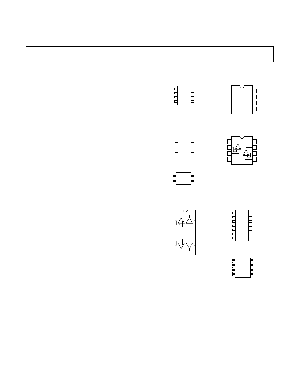
PIN CONFIGURATIONS
8-Lead SO 8-Lead Epoxy DIP
(S Suffix) (P Suffix)
8-Lead SO 8-Lead Epoxy DIP
(S Suffix) (P Suffix)
8-Lead TSSOP
(RU Suffix)
1
8
OP281
4
5
14-Lead Epoxy DIP 14-Lead
(P Suffix) Narrow-Body SO
14-Lead TSSOP
NOTE: PIN ORIENTATION IS EQUIVALENT FOR
EACH PACKAGE VARIATION
(S Suffix)
(RU Suffix)
1
14
OP481
78
REV. 0
Information furnished by Analog Devices is believed to be accurate and
reliable. However, no responsibility is assumed by Analog Devices for its
use, nor for any infringements of patents or other rights of third parties
which may result from its use. No license is granted by implication or
otherwise under any patent or patent rights of Analog Devices.
One Technology Way, P.O. Box 9106, Norwood, MA 02062-9106, U.S.A.
Tel: 617/329-4700 World Wide Web Site: http://www.analog.com
Fax: 617/326-8703 © Analog Devices, Inc., 1996

OP181/OP281/OP481–SPECIFICATIONS
ELECTRICAL SPECIFICATIONS
(@ VS = +3.0 V, VCM = 1.5 V, TA = +258C unless otherwise noted)
Parameter Symbol Conditions Min Typ Max Units
INPUT CHARACTERISTICS
Offset Voltage V
Input Bias Current I
Input Offset Current I
OS
B
OS
Note 1 1.5 mV
–40°C ≤ T
≤ +85°C 2.5 mV
A
–40°C ≤ TA ≤ +85°C310nA
–40°C ≤ TA ≤ +85°C 0.1 7 nA
Input Voltage Range 0 2 V
Common-Mode Rejection Ratio CMRR V
Large Signal Voltage Gain A
Offset Voltage Drift ∆V
Bias Current Drift ∆I
VO
/∆T10µV/°C
OS
/∆T 20 pA/°C
B
= 0 V to 2.0 V,
CM
–40°C ≤ T
R
= 1 MΩ, V
L
–40°C ≤ T
≤ +85°C6595 dB
A
= 0.3 V to 2.7 V 5 13 V/mV
O
≤ +85°C 2 V/mV
A
Offset Current Drift ∆IOS/∆T 2 pA/°C
OUTPUT CHARACTERISTICS
Output Voltage High V
Output Voltage Low V
Short Circuit Limit I
OH
OL
SC
R
= 100 kΩ to GND,
L
–40°C ≤ T
R
= 100 kΩ to V+,
L
–40°C ≤ T
≤ +85°C 2.925 2.96 V
A
≤ +85°C2575mV
A
±1.1 mA
POWER SUPPLY
Power Supply Rejection Ratio PSRR V
Supply Current/Amplifier I
SY
= 2.7 V to 12 V
S
–40°C ≤ T
V
= 0 V 3 4 µA
O
≤ +85°C7695 dB
A
–40°C ≤ TA ≤ +85°C5µA
DYNAMIC PERFORMANCE
Slew Rate SR R
Turn On Time A
Turn On Time A
= 100 kΩ, C
L
= 1, V
V
= 20, V
V
= 1 40 µs
O
O
= 50 pF 25 V/ms
L
= 1 50 µs
Saturation Recovery Time 65 µs
Gain Bandwidth Product GBP 95 kHz
Phase Margin φo 70 Degrees
NOISE PERFORMANCE
Voltage Noise e
Voltage Noise Density e
Current Noise Density i
NOTES
1
VOS is tested under no load condition.
Specifications subject to change without notice.
p-p 0.1 Hz to 10 Hz 10 µV p-p
n
n
n
f = 1 kHz 75 nV/√Hz
<1 pA/√Hz
–2–
REV. 0

OP181/OP281/OP481
ELECTRICAL SPECIFICATIONS
(@ VS = +5.0 V, VCM = 2.5 V, TA = +258C unless otherwise noted1)
Parameter Symbol Conditions Min Typ Max Units
INPUT CHARACTERISTICS
Offset Voltage V
Input Bias Current I
Input Offset Current I
OS
B
OS
Note 1 0.1 1.5 mV
–40°C ≤ T
≤ +85°C 2.5 mV
A
–40°C ≤ TA ≤ +85°C310nA
–40°C ≤ TA ≤ +85°C 0.1 7 nA
Input Voltage Range 0 4 V
Common-Mode Rejection Ratio CMRR V
Large Signal Voltage Gain A
Offset Voltage Drift ∆V
Bias Current Drift ∆I
VO
/∆T –40°C to +85°C10µV/°C
OS
/∆T20pA/°C
B
= 0 V to 4.0 V,
CM
–40°C ≤ T
R
= 1 MΩ , V
L
–40°C ≤ T
≤ +85°C6590 dB
A
= 0.5 V to 4.5 V 5 15 V/mV
O
≤ +85°C 2 V/mV
A
Offset Current Drift ∆IOS/∆T2pA/°C
OUTPUT CHARACTERISTICS
Output Voltage High V
Output Voltage Low V
Short Circuit Limit I
OH
OL
SC
R
= 100 kΩ to GND,
L
–40°C ≤ T
R
= 100 kΩ to V+,
L
–40°C ≤ T
≤ +85°C 4.925 4.96 V
A
≤ +85°C2575mV
A
±3.5 mA
POWER SUPPLY
Power Supply Rejection Ratio PSRR V
Supply Current/Amplifier I
SY
= 2.7 V to 12 V,
S
–40°C ≤ T
V
= 0 V 3.2 4 µA
O
≤ +85°C7695 dB
A
–40°C ≤ TA ≤ +85°C5µA
DYNAMIC PERFORMANCE
Slew Rate SR R
= 100 kΩ, C
L
= 50 pF 27 V/ms
L
Saturation Recovery Time 120 µs
Gain Bandwidth Product GBP 100 kHz
Phase Margin φo 74 Degrees
NOISE PERFORMANCE
Voltage Noise e
Voltage Noise Density e
Current Noise Density i
NOTES
1
VOS is tested under a no load condition.
Specifications subject to change without notice.
p-p 0.1 Hz to 10 Hz 10 µV p-p
n
n
n
f = 1 kHz 75 nV/√Hz
<1 pA/√Hz
REV. 0
–3–

OP181/OP281/OP481–SPECIFICATIONS
ELECTRICAL SPECIFICATIONS
(@ VS = ±5 V, TA = +258C unless otherwise noted)
Parameter Symbol Conditions Min Typ Max Units
INPUT CHARACTERISTICS
Offset Voltage V
Input Bias Current I
Input Offset Current I
OS
B
OS
Note 1 0.1 1.5 mV
–40°C ≤ T
≤ +85°C 2.5 mV
A
–40°C ≤ TA ≤ +85°C310nA
–40°C ≤ TA ≤ +85°C 0.1 7 nA
Input Voltage Range –5 +4 V
Common-Mode Rejection CMRR V
Large Signal Voltage Gain A
Offset Voltage Drift ∆V
Bias Current Drift ∆I
VO
/∆T –40°C to +85°C10µV/°C
OS
/∆T 20 pA/°C
B
= –5.0 V to +4.0 V,
CM
–40°C ≤ T
R
= 1 MΩ, VO = ±4.0 V, 5 13 V/mV
L
–40°C ≤ T
≤ +85°C6595dB
A
≤ +85°C 2 V/mV
A
Offset Current Drift ∆IOS/∆T 2 pA/°C
OUTPUT CHARACTERISTICS
Output Voltage Swing V
Short Circuit Limit I
O
SC
R
= 100 kΩ to GND,
L
–40°C ≤ T
≤ +85°C ±4.925 ±4.98 V
A
12 mA
POWER SUPPLY
Power Supply Rejection Ratio PSRR V
Supply Current/Amplifier I
SY
= ±1.35 V to ±6V,
S
–40°C ≤ T
V
= 0 V 3.3 5 µA
O
≤ +85°C7695dB
A
–40°C ≤ TA ≤ +85°C6µA
DYNAMIC PERFORMANCE
Slew Rate ±SR R
= 100 kΩ, C
L
= 50 pF 28 V/ms
L
Gain Bandwidth Product GBP 105 kHz
Phase Margin φo 75 Degrees
NOISE PERFORMANCE
Voltage Noise e
Voltage Noise Density e
Voltage Noise Density e
Current Noise Density i
NOTES
1
VOS is tested under no load condition.
Specifications subject to change without notice.
p-p 0.1 Hz to 10 Hz 10 µV p-p
n
n
n
n
f = 1 kHz 85 nV/√Hz
f = 10 kHz 75 nV/√Hz
<1 pA/√Hz
–4–
REV. 0

OP181/OP281/OP481
WARNING!
ESD SENSITIVE DEVICE
ABSOLUTE MAXIMUM RATINGS
Supply Voltage . . . . . . . . . . . . . . . . . . . . . . . . . . . . . . . . +16 V
Input Voltage . . . . . . . . . . . . . . . . . . . . . . . . Gnd to V
+ 10 V
S
Differential Input Voltage . . . . . . . . . . . . . . . . . . . . . . . ±3.5 V
Output Short-Circuit Duration to Gnd . . . . . . . . . . Indefinite
Storage Temperature Range
P, S, RU Package . . . . . . . . . . . . . . . . . . . –65°C to +150°C
Operating Temperature Range
OP181/OP281/OP481G . . . . . . . . . . . . . . . –40°C to +85°C
Junction Temperature Range
P, S, RU Package . . . . . . . . . . . . . . . . . . . –65°C to +150°C
Lead Temperature Range (Soldering, 60 sec) . . . . . . . +300°C
Package Type uJA* u
JC
Units
8-Pin Plastic DIP (P) 103 43 °C/W
8-Pin SOIC (S) 158 43 °C/W
8-Pin TSSOP (RU) 240 43 °C/W
14-Pin Plastic DIP (P) 76 33 °C/W
14-Pin SOIC (S) 120 36 °C/W
14-Pin TSSOP (RU) 240 43 °C/W
*θJA is specified for the worst case conditions, i.e., θJA is specified for device in socket
for P-DIP packages; θJA is specified for device soldered in circuit board for TSSOP
and SOIC packages.
ORDERING GUIDE
Temperature Package Package
Model Range Description Option
OP181GP –40°C to +85°C 8-Pin Plastic DIP N-8
OP181GS –40°C to +85°C 8-Pin SOIC SO-8
OP281GP –40°C to +85°C 8-Pin Plastic DIP N-8
OP281GS –40°C to +85°C 8-Pin SOIC SO-8
OP281GRU –40°C to +85°C 8-Pin TSSOP RU-8
OP481GP –40°C to +85°C 14-Pin Plastic DIP N-14
OP481GS –40°C to +85°C 14-Pin SOIC SO-14
OP481GRU –40°C to +85°C 14-Pin TSSOP RU-14
CAUTION
ESD (electrostatic discharge) sensitive device. Electrostatic charges as high as 4000 V readily
accumulate on the human body and test equipment and can discharge without detection. Although
the OP181/OP281/OP481 features proprietary ESD protection circuitry, permanent damage may
occur on devices subjected to high energy electrostatic discharges. Therefore, proper ESD precautions are recommended to avoid performance degradation or loss of functionality.
REV. 0
–5–
 Loading...