


a |
Micropower Single-Supply |
|
Rail-to-Rail Input/Output Op Amps |
||
|
|
OP191/OP291/OP491 |
|
|
|
FEATURES
Single-Supply Operation: 2.7 V to 12 V
Wide Input Voltage Range
Rail-to-Rail Output Swing
Low Supply Current: 300 μA/Amp
Wide Bandwidth: 3 MHz
Slew Rate: 0.5 V/μs
Low Offset Voltage: 700 μV
No Phase Reversal
APPLICATIONS
Industrial Process Control
Battery Powered Instrumentation
Power Supply Control and Protection
Telecom
Remote Sensors
Low Voltage Strain Gage Amplifiers
DAC Output Amplifier
GENERAL DESCRIPTION
The OP191, OP291 and OP491 are single, dual and quad micropower, single-supply, 3 MHz bandwidth amplifiers featuring rail-to-rail inputs and outputs. All are guaranteed to operate from a 3 volt single supply as well as ±5 volt dual supplies.
Fabricated on Analog Devices’ CBCMOS process, the OP191 family has a unique input stage that allows the input voltage to safely extend 10 volts beyond either supply without any phase inversion or latch-up. The output voltage swings to within millivolts of the supplies and continues to sink or source current all the way to the supplies.
Applications for these amplifiers include portable telecom equipment, power supply control and protection, and interface for transducers with wide output ranges. Sensors requiring a rail-to-rail input amplifier include Hall effect, piezo electric, and resistive transducers.
The ability to swing rail-to-rail at both the input and output enables designers to build multistage filters in single-supply systems and maintain high signal-to-noise ratios.
The OP191/OP291/OP491 are specified over the extended industrial (–40°C to +125°C) temperature range. The OP191 single and OP291 dual amplifiers are available in 8-pin plastic DIPs and SO surface mount packages. The OP491 quad is available in 14-pin DIPs and narrow 14-pin SO packages. Consult factory for OP491 TSSOP availability.
REV. 0
Information furnished by Analog Devices is believed to be accurate and reliable. However, no responsibility is assumed by Analog Devices for its use, nor for any infringements of patents or other rights of third parties which may result from its use. No license is granted by implication or otherwise under any patent or patent rights of Analog Devices.
OP191/OP291/OP491 PIN CONFIGURATIONS
8-Lead Narrow-Body SO |
8-Lead Epoxy DIP |
(S Suffix) |
(P Suffix) |
1 |
|
8 |
NC |
1 |
OP191 |
8 |
NC |
|
2 |
OP191 |
7 |
||||||
–INA |
2 |
|
7 |
V+ |
||||
3 |
|
6 |
|
|
|
|
|
|
4 |
|
5 |
+INA |
3 |
|
6 |
OUTA |
|
|
|
|
–V |
4 |
|
5 |
NC |
|
|
|
|
|
|
NC = NO CONNECT |
|
|
8-Lead Narrow-Body SO |
8-Lead Epoxy DIP |
(S Suffix) |
(P Suffix) |
1 |
|
8 |
OUTA |
1 |
OP291 |
8 |
+V |
32 |
|
67 |
|||||
OP291 |
–INA |
2 |
|
7 |
OUTB |
||
4 |
|
5 |
+INA |
3 |
|
6 |
–INB |
|
|
|
–V |
4 |
|
5 |
+INB |
14-Lead Epoxy DIP
(P Suffix)
OUTA |
1 |
|
14 |
OUTD |
–INA |
2 |
|
13 |
–IND |
+INA |
3 |
|
12 |
+IND |
+V |
4 |
OP491 |
11 |
–V |
+INB |
5 |
|
10 |
+INC |
–INB |
6 |
|
9 |
–INC |
OUTB |
7 |
|
8 |
OUTC |
14-Lead SO
(S Suffix)
|
|
|
|
|
OUTA |
1 |
|
14 |
OUTD |
–INA |
|
|
|
–IND |
2 |
|
13 |
||
|
|
|
|
+IND |
+INA |
3 |
|
12 |
|
+V |
|
|
|
–V |
4 |
OP491 |
11 |
||
+INB |
5 |
|
10 |
+INC |
|
|
|
|
–INC |
–INB |
6 |
|
9 |
|
|
|
|
|
OUTC |
OUTB |
7 |
|
8 |
|
|
|
|
|
|
14-Lead TSSOP (RU Suffix)
1 |
14 |
213
312
4 |
OP491 |
11 |
510
69
78
One Technology Way, P.O. Box 9106, Norwood. MA 02062-9106, U.S.A. Tel: 617/329-4700 Fax: 617/326-8703
OP191/OP291/OP491–SPECIFICATIONS
ELECTRICAL SPECIFICATIONS(@ VS = +3.0 V, VCM = 0.1 V, VO = 1.4 V, TA = +25°C unless otherwise noted)
Parameter |
|
Symbol |
Conditions |
Min |
Typ |
Max |
Units |
||
|
|
|
|
|
|
|
|
|
|
INPUT CHARACTERISTICS |
|
|
|
|
|
mV |
|||
Offset Voltage |
OP191G |
VOS |
–40 £ TA £ +125°C |
|
80 |
500 |
|||
|
|
|
|
|
1 |
mV |
|||
|
OP291/OP491G |
VOS |
–40 £ TA £ +125°C |
|
80 |
700 |
mV |
||
Input Bias Current |
|
IB |
|
|
1.25 |
mV |
|||
|
–40 £ TA £ +125°C |
|
30 |
50 |
nA |
||||
Input Offset Current |
IOS |
|
|
70 |
nA |
||||
–40 £ TA £ +125°C |
|
0.1 |
8 |
nA |
|||||
|
|
|
|
|
16 |
nA |
|||
Input Voltage Range |
|
|
0 |
|
3 |
V |
|||
Common-Mode Rejection Ratio |
CMRR |
VCM = 0 V to 2.9 V |
70 |
90 |
|
dB |
|||
|
|
|
–40 £ TA £ +125°C |
65 |
87 |
|
dB |
||
Large Signal Voltage Gain |
AVO |
RL = 10 kW , VO = 0.3 V to 2.7 V |
25 |
70 |
|
V/mV |
|||
|
|
DVOS/DT |
–40 £ TA £ +125°C |
|
50 |
|
V/mV |
||
Offset Voltage Drift |
|
|
1.1 |
|
mV/°C |
||||
Bias Current Drift |
|
DIB/DT |
|
|
100 |
|
pA/°C |
||
Offset Current Drift |
DIOS/DT |
|
|
20 |
|
pA/°C |
|||
OUTPUT CHARACTERISTICS |
|
RL = 100 kW to GND |
|
|
|
|
|
|
|
Output Voltage High |
VOH |
2.95 |
2.99 |
|
V |
||||
|
|
|
–40°C to +125°C |
2.90 |
2.98 |
|
V |
||
|
|
|
RL = 2 kW to GND |
2.8 |
2.9 |
|
V |
||
|
|
|
–40°C to +125°C |
2.70 |
2.8 |
|
V |
||
Output Voltage Low |
VOL |
RL = 100 kW to V+ |
|
4.5 |
10 |
mV |
|||
|
|
|
–40°C to +125°C |
|
|
35 |
mV |
||
|
|
|
RL = 2 kW to V+ |
|
40 |
75 |
mV |
||
Short Circuit Limit |
ISC |
–40°C to +125°C |
± 8.75 |
± 13.5 |
130 |
mV |
|||
Sink/Source |
|
mA |
|||||||
|
|
|
–40°C to +125°C |
± 6.0 |
± 10.5 |
|
mA |
||
Open Loop Impedance |
ZOUT |
f = 1 MHz, AV = 1 |
|
200 |
|
W |
|||
POWER SUPPLY |
|
|
|
|
|
|
|
|
|
Power Supply Rejection Ratio |
PSRR |
VS = 2.7 V to 12 V |
80 |
110 |
|
dB |
|||
|
|
|
–40°C £ TA £ +125°C |
75 |
110 |
|
dB |
||
Supply Current/Amplifier |
ISY |
VO = 0 V |
|
200 |
350 |
mA |
|||
|
|
|
–40°C £ TA £ +125°C |
|
330 |
480 |
mA |
||
DYNAMIC PERFORMANCE |
|
RL = 10 kW |
|
|
|
V/ms |
|||
Slew Rate |
|
+SR |
|
0.4 |
|
||||
Slew Rate |
|
–SR |
RL = 10 kW |
|
0.4 |
|
V/ms |
||
Full-Power Bandwidth |
BWP |
1% Distortion |
|
1.2 |
|
kHz |
|||
Settling Time |
|
tS |
To 0.01% |
|
22 |
|
ms |
||
Gain Bandwidth Product |
GBP |
|
|
3 |
|
MHz |
|||
Phase Margin |
|
qO |
f = 1 kHz, RL = 10 kW |
|
45 |
|
Degrees |
||
Channel Separation |
CS |
|
145 |
|
dB |
||||
NOISE PERFORMANCE |
|
|
|
|
|
mV p-p |
|||
Voltage Noise |
|
en p-p |
0.1 Hz to 10 Hz |
|
2 |
|
|||
Voltage Noise Density |
en |
f = 1 kHz |
|
35 |
|
nV/Ö |
Hz |
|
|
Current Noise Density |
in |
|
|
0.8 |
|
pA/ÖHz |
|||
Specifications subject to change without notice.
–2– |
REV. 0 |
OP191/OP291/OP491
ELECTRICAL SPECIFICATIONS (@ VS = +5.0 V, VCM = 0.1 V, VO = 1.4 V, TA = +25°C unless otherwise noted)
Parameter |
|
Symbol |
Conditions |
Min |
Typ |
Max |
Units |
|||
|
|
|
|
|
|
|
|
|
|
|
INPUT CHARACTERISTICS |
|
|
|
|
|
|
mV |
|||
Offset Voltage |
OP191 |
VOS |
–40 £ TA £ +125°C |
|
80 |
500 |
||||
|
|
|
|
|
1.0 |
mV |
||||
|
OP291/OP491 |
VOS |
–40 £ TA £ +125°C |
|
80 |
700 |
mV |
|||
Input Bias Current |
|
IB |
|
|
1.25 |
mV |
||||
|
–40 £ TA £ +125°C |
|
30 |
50 |
nA |
|||||
Input Offset Current |
IOS |
|
|
60 |
nA |
|||||
–40 £ TA £ +125°C |
|
0.1 |
8 |
nA |
||||||
|
|
|
|
|
16 |
nA |
||||
Input Voltage Range |
|
|
|
0 |
|
5 |
V |
|||
Common-Mode Rejection Ratio |
CMRR |
VCM = 0 V to 4.9 V |
70 |
93 |
|
dB |
||||
|
|
|
–40 £ TA £ +125°C |
65 |
90 |
|
dB |
|||
Large Signal Voltage Gain |
AVO |
RL = 10 kW , VO = 0.3 V to 4.7 V |
25 |
70 |
|
V/mV |
||||
|
|
DVOS/DT |
–40 £ TA |
£ +125°C |
|
50 |
|
V/mV |
||
Offset Voltage Drift |
–40 £ TA |
£ +125°C |
|
1.1 |
|
mV/°C |
||||
Bias Current Drift |
|
DIB/DT |
|
|
|
100 |
|
pA/°C |
||
Offset Current Drift |
DIOS/DT |
|
|
|
20 |
|
pA/°C |
|||
OUTPUT CHARACTERISTICS |
|
RL = 100 kW to GND |
|
|
|
|
|
|
||
Output Voltage High |
VOH |
4.95 |
4.99 |
|
V |
|||||
|
|
|
–40°C to +125°C |
4.90 |
4.98 |
|
V |
|||
|
|
|
RL = 2 kW to GND |
4.8 |
4.85 |
|
V |
|||
|
|
|
–40°C to +125°C |
4.65 |
4.75 |
|
V |
|||
Output Voltage Low |
VOL |
RL = 100 kW to V+ |
|
4.5 |
10 |
mV |
||||
|
|
|
–40°C to +125°C |
|
|
35 |
mV |
|||
|
|
|
RL = 2 kW to V+ |
|
40 |
75 |
mV |
|||
Short Circuit Limit |
ISC |
–40°C to +125°C |
± 8.75 |
± 13.5 |
155 |
mV |
||||
Sink/Source |
|
mA |
||||||||
|
|
|
–40°C to +125°C |
± 6.0 |
± 10.5 |
|
mA |
|||
Open Loop Impedance |
ZOUT |
f = 1 MHz, AV = 1 |
|
200 |
|
W |
||||
POWER SUPPLY |
|
|
|
|
|
|
|
|
|
|
Power Supply Rejection Ratio |
PSRR |
VS = 2.7 V to 12 V |
80 |
110 |
|
dB |
||||
|
|
|
–40 £ TA |
£ +125°C |
75 |
110 |
|
dB |
||
Supply Current/Amplifier |
ISY |
VO = 0 V |
|
|
220 |
400 |
mA |
|||
|
|
|
–40 £ TA £ +125°C |
|
350 |
500 |
mA |
|||
DYNAMIC PERFORMANCE |
|
RL = 10 kW |
|
|
|
V/ms |
||||
Slew Rate |
|
+SR |
|
0.4 |
|
|||||
Slew Rate |
|
–SR |
RL = 10 kW |
|
0.4 |
|
V/ms |
|||
Full-Power Bandwidth |
BWP |
1% Distortion |
|
1.2 |
|
kHz |
||||
Settling Time |
|
tS |
To 0.01% |
|
22 |
|
ms |
|||
Gain Bandwidth Product |
GBP |
|
|
|
3 |
|
MHz |
|||
Phase Margin |
|
qO |
f = 1 kHz, RL = 10 kW |
|
45 |
|
Degrees |
|||
Channel Separation |
CS |
|
145 |
|
dB |
|||||
NOISE PERFORMANCE |
|
|
|
|
|
|
mV p-p |
|||
Voltage Noise |
|
en p-p |
0.1 Hz to 10 Hz |
|
2 |
|
||||
Voltage Noise Density |
en |
f = 1 kHz |
|
|
35 |
|
nV/Ö |
Hz |
|
|
Current Noise Density |
in |
|
|
|
0.8 |
|
pA/ÖHz |
|||
NOTES
+5 V specifications are guaranteed by +3 V and ±5 V testing. Specifications subject to change without notice.
REV. 0 |
–3– |
OP191/OP291/OP491
ELECTRICAL SPECIFICATIONS (@ VO = ±5.0 V, –4.9 V ≤ VCM ≤ +4.9 V, TA = +25°C unless otherwise noted)
Parameter |
|
Symbol |
|
Conditions |
Min |
Typ |
Max |
Units |
|||||||||
|
|
|
|
|
|
|
|
|
|
|
|
|
|
|
|
|
|
INPUT CHARACTERISTICS |
|
|
|
|
|
|
|
|
|
|
|
mV |
|||||
Offset Voltage |
OP191 |
VOS |
|
–40 £ TA £ +125°C |
|
80 |
500 |
||||||||||
|
|
|
|
|
|
|
|
|
|
1 |
mV |
||||||
|
OP291/OP491 |
VOS |
|
–40 £ TA £ +125°C |
|
80 |
700 |
mV |
|||||||||
Input Bias Current |
|
IB |
|
|
|
1.25 |
mV |
||||||||||
|
|
–40 £ TA £ +125°C |
|
30 |
50 |
nA |
|||||||||||
Input Offset Current |
IOS |
|
|
|
70 |
nA |
|||||||||||
|
–40 £ TA £ +125°C |
|
0.1 |
8 |
nA |
||||||||||||
|
|
|
|
|
|
|
|
|
|
16 |
nA |
||||||
Input Voltage Range |
|
|
|
|
|
|
VCM = ± 5 V |
–5 |
|
+5 |
V |
||||||
Common-Mode Rejection |
CMR |
|
75 |
100 |
|
dB |
|||||||||||
|
|
|
|
|
|
|
|
–40 £ TA £ +125°C |
67 |
97 |
|
dB |
|||||
Large Signal Voltage Gain |
AVO |
|
RL = 10 kW, VO = ±4.7 V, |
25 |
70 |
|
|
|
|
|
|
||||||
|
|
DVOS/DT |
|
–40 £ TA £ +125°C |
|
50 |
|
V/mV |
|||||||||
Offset Voltage Drift |
|
|
|
|
|
1.1 |
|
mV/°C |
|||||||||
Bias Current Drift |
|
DIB/DT |
|
|
|
|
100 |
|
pA/°C |
||||||||
Offset Current Drift |
|
DIOS/DT |
|
|
|
|
20 |
|
pA/°C |
||||||||
OUTPUT CHARACTERISTICS |
|
|
|
|
|
|
RL = 100 kW to GND |
± 4.93 |
± 4.99 |
|
|
|
|
|
|
||
Output Voltage Swing |
VO |
|
|
V |
|||||||||||||
|
|
|
|
|
|
|
|
–40°C to +125°C |
± 4.90 |
± 4.98 |
|
V |
|||||
|
|
|
|
|
|
|
|
RL = 2 kW to GND |
± 4.80 |
± 4.95 |
|
V |
|||||
|
|
|
|
|
|
|
|
–40 £ TA £ +125°C |
± 4.65 |
± 4.75 |
|
V |
|||||
Short Circuit Limit |
|
ISC |
|
Sink/Source |
± 8.75 |
± 16 |
|
mA |
|||||||||
|
|
|
|
|
|
|
|
–40°C to +125°C |
± 6 |
± 13 |
|
mA |
|||||
Open Loop Impedance |
ZOUT |
|
f = 1 MHz, AV = 1 |
|
200 |
|
W |
||||||||||
POWER SUPPLY |
|
|
|
|
|
|
|
VS = ± 5 V |
|
|
|
|
|
|
|
|
|
Power Supply Rejection Ratio |
PSRR |
|
80 |
110 |
|
dB |
|||||||||||
|
|
|
|
|
|
|
|
–40 £ TA £ +125°C |
70 |
100 |
|
dB |
|||||
Supply Current/Amplifier |
ISY |
|
VO = 0 V |
|
260 |
420 |
mA |
||||||||||
|
|
|
|
|
|
|
|
–40 £ TA £ +125°C |
|
390 |
550 |
mA |
|||||
DYNAMIC PERFORMANCE |
± SR |
|
RL =10 kW |
|
|
|
V/ms |
||||||||||
Slew Rate |
|
|
|
0.5 |
|
||||||||||||
Full-Power Bandwidth |
BWP |
|
1% Distortion |
|
1.2 |
|
kHz |
||||||||||
Settling Time |
|
tS |
|
To 0.01% |
|
22 |
|
ms |
|||||||||
Gain Bandwidth Product |
GBP |
|
|
|
|
3 |
|
MHz |
|||||||||
Phase Margin |
|
qO |
|
|
|
|
45 |
|
Degrees |
||||||||
Channel Separation |
|
CS |
|
f = 1 kHz |
|
145 |
|
dB |
|||||||||
|
|
|
|
|
|
|
|
|
|
|
|
|
|
|
|
|
|
NOISE PERFORMANCE |
|
|
|
|
|
|
|
|
|
|
|
mV p-p |
|||||
Voltage Noise |
|
en p-p |
|
0.1 Hz to 10 Hz |
|
2 |
|
||||||||||
Voltage Noise Density |
en |
|
f = 1 kHz |
|
35 |
|
nV/Ö |
Hz |
|
||||||||
Current Noise Density |
in |
|
|
|
|
0.8 |
|
pA/Ö |
|
|
|||||||
|
|
|
|
Hz |
|||||||||||||
Specifications subject to change without notice. |
|
|
|
|
|
|
|
|
|
|
|
|
|
|
|
|
|
|
|
|
|
|
|
5V |
VS = ±5V |
|
|
|
|
|
|
|
|
|
|
|
|
|
100 |
|
|
|
RL = 2kΩ |
|
|
|
|
|
|
|
|
|
|
|
|
|
|
|
|
|
|
AV = +1 |
|
|
|
|
|
|
|
|
|
|
|
|
|
90 |
|
|
|
VIN = 20Vp-p |
|
|
|
|
|
|
|
|
|
|
|
INPUT |
|
|
|
|
|
|
|
|
|
|
|
|
|
|
|
|
|
|
|
|
|
|
|
|
|
|
|
|
|
|
|
||
|
|
OUTPUT |
|
|
|
|
|
|
|
|
|
|
|
|
|
|
|
|
|
|
|
|
|
|
|
|
|
|
|
|
|
|
|
|
|
|
|
|
10 |
|
|
|
|
|
|
|
|
|
|
|
|
|
|
|
|
|
|
|
|
|
|
|
|
|
|
|
|
|
|
|
|
|
|
|
0% |
|
|
|
|
|
|
|
|
|
|
|
|
|
|
|
|
|
|
|
|
|
200µs |
|
|
|
|
|
|
|
|
|
|
|
|
|
|
|
|
5V |
|
|
|
|
|
|
|
|
|
||
|
|
|
|
|
|
|
|
|
|
|
|
|
|
|
|
|
|
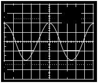
Figure 1. Input and Output with Inputs Overdriven by 5 V
–4– |
REV. 0 |

OP191/OP291/OP491
WAFER TEST LIMITS (@ VS = +3.0 V, VCM = 0.1 V, TA = +25°C unless otherwise noted)
Parameter |
Symbol |
Conditions |
Limit |
Units |
|
|
|
|
|
Offset Voltage |
VOS |
|
±300 |
μV max |
Input Bias Current |
IB |
|
50 |
nA max |
Input Offset Current |
IOS |
|
8 |
nA |
Input Voltage Range |
VCM |
|
V– to V+ |
V min |
Common-Mode Rejection Ratio |
CMRR |
VCM = 0 V to +2.9 V |
70 |
dB min |
Power Supply Rejection Ratio |
PSRR |
V = 2.7 V to +12 V |
80 |
dB min |
Large Signal Voltage Gain |
AVO |
RL = 10 kΩ |
50 |
V/mV min |
Output Voltage High |
VOH |
RL = 2 kΩ to GND |
2.8 |
V min |
Output Voltage Low |
VOL |
RL = 2 kΩ to V+ |
75 |
mV max |
Supply Current/Amplifier |
ISY |
VO = 0 V, RL = ∞ |
350 |
μA max |
NOTE
Electrical tests and wafer probe to the limits shown. Due to variations in assembly methods and normal yield loss, yield after packaging is not guaranteed for standard product dice. Consult factory to negotiate specifications based on dice lot qualifications through sample lot assembly and testing.
ABSOLUTE MAXIMUM RATINGS1
Supply Voltage . . . . . . . . . . . . . . . . . . . . . . . . . . . . . . . . +16 V
Input Voltage . . . . . . . . . . . . . . . . . . . . . . . .GND to VS + 10 V Differential Input Voltage . . . . . . . . . . . . . . . . . . . . . . . . . . 7 V
Output Short-Circuit Duration to GND . . . . . . . . . . Indefinite Storage Temperature Range
P, S, RU Packages . . . . . . . . . . . . . . . . . . . –65°C to +150°C Operating Temperature Range
OP191/OP291/OP491G . . . . . . . . . . . . . . . –40°C to +125°C Junction Temperature Range
P, S, RU Packages . . . . . . . . . . . . . . . . . . . –65°C to +150°C Lead Temperature Range (Soldering 60 sec) . . . . . . . . +300°C
Package Type |
θJA2 |
θJC |
Units |
|
|
|
|
8-Pin Plastic DIP (P) |
103 |
43 |
°C/W |
8-Pin SOIC (S) |
158 |
43 |
°C/W |
14-Pin Plastic DIP (P) |
76 |
33 |
°C/W |
14-Pin SOIC (S) |
120 |
36 |
°C/W |
14-Pin TSSOP (RU) |
180 |
35 |
°C/W |
NOTES
1Absolute maximum ratings apply to both DICE and packaged parts, unless otherwise noted.
2θJA is specified for the worst case conditions; i.e., θJA is specified for device in socket for P-DIP packages; θJA is specified for device soldered in circuit board for TSSOP and SOIC packages.
ORDERING GUIDE
|
Temperature |
Package |
Package |
Model |
Range |
Description |
Option |
|
|
|
|
OP191GP |
–40°C to +125°C |
8-Pin Plastic DIP |
N-8 |
OP191GS |
–40°C to +125°C |
8-Pin SOIC |
SO-8 |
OP191GBC |
+25°C |
DICE |
|
OP291GP |
–40°C to +125°C |
8-Pin Plastic DIP |
N-8 |
OP291GS |
–40°C to +125°C |
8-Pin SOIC |
SO-8 |
OP291GBC |
+25°C |
DICE |
|
OP491GP |
–40°C to +125°C |
14-Pin Plastic DIP |
N-14 |
OP491GS |
–40°C to +125°C |
14-Pin SOIC |
SO-14 |
OP491HRU |
–40°C to +125°C |
14-Pin TSSOP |
RU-14 |
OP491GBC |
+25°C |
DICE |
|
2 |
1 |
14 |
13 |
DICE CHARACTERISTICS
7
2
6
3
4
OP191 Die Size 0.047 × 0.066 Inch, 3,102 Sq. Mils. Substrate (Die Backside) Is Connected to V+.
Transistor Count, 74.
1 |
8 |
7 |
|
|
|
|||||
2 |
|
|
|
|
|
|
|
|
|
6 |
|
|
|
|
|
|
|
||||
|
|
|
|
|
|
|
||||
3 |
|
|
|
|
|
|
|
|
5 |
|
|
|
|
|
|
|
|||||
|
|
|
|
|
|
|
|
|
|
|
|
|
|
|
|
|
|
|
|
|
|
|
|
|
|
4 |
|
|
|
|
|
|
OP291 Die Size 0.070 × 0.070 Inch, 4,900 Sq. Mils. Substrate (Die Backside) Is Connected to V+.
Transistor Count, 146
3 |
|
|
|
|
12 |
|
|
|
|||
4 |
|
|
11 |
||
|
|||||
5 |
|
|
|
|
|
|
|
|
|
|
10 |
|
|
|
|
|
|
|
|
||||
|
|
|
|
|
|
|
|
|
|||
|
|
|
|
|
|
|
|
|
|
||
6 |
7 |
8 |
9 |
|
|
||||||
OP491 Die Size 0.070 × 0.110 Inch, 7,700 Sq. Mils. Substrate (Die Backside) Is Connected to V+. Transistor Count, 290.
REV. 0 |
–5– |

OP191/OP291/OP491–Typical Performance Characteristics
UNITS
180
VS = +3V 160 TA = +25°C
BASED ON 1200 140 OP AMPS
120
100
80
60
40
20
0 


 –0.18 –0.10 –0.02 0.06 0.14 0.22
INPUT OFFSET VOLTAGE – mV
UNITS
120
VS = +3V
100  –40°C < TA < +125°C
BASED ON 600 OP AMPS
80
60 |
|
|
|
|
|
|
|
40 |
|
|
|
|
|
|
|
20 |
|
|
|
|
|
|
|
0 |
|
|
|
|
|
|
|
0 |
1 |
2 |
3 |
4 |
5 |
6 |
7 |
|
|
INPUT OFFSET VOLTAGE – µV/ °C |
|
||||
|
0 |
|
|
|
|
VS = +3V |
|
|
|
– mV |
–0.02 |
|
VCM = 0.1V |
|
|
|
|
|
|
VOLTAGE |
–0.04 |
|
|
|
–0.06 |
|
VCM = 0V |
|
|
|
|
|
||
|
|
VCM = 3V |
|
|
OFFSET |
|
|
|
|
–0.08 |
|
|
|
|
–0.1 |
|
|
|
|
INPUT |
|
|
|
|
|
|
VCM = 2.9V |
|
|
–0.12 |
|
|
|
|
|
|
|
|
|
|
–0.14 |
|
85 |
|
|
–40 |
25 |
125 |
|
|
|
TEMPERATURE – °C |
|
|
Figure 2. OP291 Input Offset Voltage
Distribution, VS = +3 V |
|
|
||
|
40 |
|
VCM = 3V |
|
|
30 |
|
|
|
|
|
|
|
|
nA |
20 |
|
VCM = 2.9V |
|
– |
10 |
|
|
|
CURRENT |
|
|
||
|
|
|
||
0 |
VS = +3V |
|
|
|
–10 |
|
|
||
|
|
|
||
BIAS |
–20 |
|
VCM = 0.1V |
|
|
|
|
||
|
|
|
|
|
INPUT |
–30 |
|
|
|
–40 |
|
|
|
|
|
|
|
|
|
|
–50 |
|
VCM = 0V |
|
|
|
|
|
|
|
–60 |
|
|
|
|
–40 |
25 |
85 |
125 |
|
|
TEMPERATURE – °C |
|
|
Figure 5. Input Bias Current vs.
Temperature, VS = +3 V |
|
|
||
|
3.00 |
|
|
|
|
|
+VO @ RL = 100k |
|
|
– Volts |
2.95 |
|
|
|
2.90 |
|
|
|
|
SWING |
|
|
|
|
|
+VO @ RL = 2k |
|
|
|
|
|
|
|
|
OUTPUT |
2.85 |
|
|
|
2.80 |
|
|
|
|
|
|
|
|
|
|
|
VS = +3V |
|
|
|
2.75 |
|
|
|
|
–40 |
25 |
85 |
125 |
|
|
TEMPERATURE – °C |
|
|
Figure 8. Output Voltage Swing vs. Temperature, VS = +3 V
Figure 3. OP291 Input Offset Volt- |
Figure 4. Input Offset Voltage vs. |
age Drift Distribution, VS = +3 V |
Temperature, VS = +3 V |
|
|
|
||||||||
|
0 |
|
|
|
36 |
|
|
|
|
|
|
|
nA– |
–0.2 |
VS = +3V |
|
nA |
30 |
VS = +3V |
|
|
|
|
|
|
–0.4 |
VCM = 0.1V |
24 |
|
|
|
|
|
|
|
|||
|
|
|
|
|
|
|
|
|
|
|
||
CURRENTOFFSETINPUT |
|
|
VCM = 2.9V |
CURRENTBIASINPUT– |
18 |
|
|
|
|
|
|
|
|
|
–24 |
|
|
|
|
|
|
|
|||
–0.6 |
|
|
|
|
|
|
|
|
|
|||
|
|
VCM = 3V |
|
12 |
|
|
|
|
|
|
|
|
|
–0.8 |
|
|
6 |
|
|
|
|
|
|
|
|
|
|
|
|
|
|
|
|
|
|
|
||
|
|
VCM = 0V |
|
|
|
|
|
|
|
|
|
|
|
–1.0 |
|
|
0 |
|
|
|
|
|
|
|
|
|
|
|
|
–6 |
|
|
|
|
|
|
|
|
|
|
|
|
|
|
|
|
|
|
|
|
|
|
–1.2 |
|
|
|
–12 |
|
|
|
|
|
|
|
|
–1.4 |
|
|
|
–18 |
|
|
|
|
|
|
|
|
|
|
|
|
|
|
|
|
|
|
|
|
|
–1.6 |
|
|
|
–30 |
|
|
|
|
|
|
|
|
|
|
|
|
|
|
|
|
|
|
|
|
|
–1.8 |
|
|
|
–36 |
|
|
|
|
|
|
|
|
–40 |
25 |
85 |
125 |
0 |
0.30 0.60 0.90 1.2 |
1.5 |
1.8 |
2.1 |
2.4 |
2.7 |
3.0 |
|
|
INPUT COMMON MODE VOLTAGE – Volts |
||||||||||
|
|
TEMPERATURE – °C |
|
|
||||||||
Figure 6. Input Offset Current |
Figure 7. Input Bias Current vs. |
vs. Temperature, VS = +3 V |
Common-Mode Voltage, VS = +3 V |
|
160 |
|
|
|
|
|
|
|
1200 |
|
|
|
|
|
|
|
|
|
|
|
|
|
|
|
|
|
140 |
|
|
|
VS = +3V |
|
|
|
|
RL = 100kΩ, |
|
|
|
|
|
|
|
° |
|
|
|
1000 |
VCM = 2.9V |
|
|
|
|
|
|
|
TA = +25 C |
|
|
|
|
|
|
|
dB–GAINLOOP-OPEN |
120 |
|
|
|
|
|
Degrees–SHIFTPHASE |
–V/mVGAINLOOP-OPEN |
|
RL = 100kΩ, |
|
|
100 |
|
|
|
|
|
800 |
|
|
||||
|
|
|
|
|
|
|
|
VCM = 0.1V |
|
|
||
|
|
|
|
|
|
|
|
|
|
|
||
|
80 |
|
|
|
|
0 |
|
|
|
|
|
|
|
|
|
|
|
|
|
|
|
|
|
|
|
|
60 |
|
|
|
|
45 |
|
|
600 |
|
|
|
|
|
|
|
|
|
|
|
|
|
|
||
|
40 |
|
|
|
|
90 |
|
|
400 |
|
|
|
|
20 |
|
|
|
|
135 |
|
|
|
|
|
|
|
|
|
|
|
|
|
|
|
|
|
||
|
0 |
|
|
|
|
180 |
|
|
200 |
|
|
|
|
|
|
|
|
|
|
|
|
|
|
||
|
–20 |
|
|
|
|
225 |
|
|
|
VS = 3V, VO = 0.3V / 2.7V |
|
|
|
–40 |
1k |
10k |
100k |
1M |
270 |
|
|
0 |
25 |
85 |
125 |
|
100 |
10M |
|
|
–40 |
|||||||
|
|
|
FREQUENCY – Hz |
|
|
|
|
TEMPERATURE – °C |
|
|||
Figure 9. Open-Loop Gain & Phase |
Figure 10. Open-Loop Gain vs. |
vs. Frequency, VS = +3 V |
Temperature, VS = +3 V |
–6– |
REV. 0 |
 Loading...