


 Loading...
Analog Devices SSM2161S-REEL, SSM2161S, SSM2161P, SSM2160S-REEL, SSM2160S Datasheet
...
6- and 4-Channel, Serial Input
a Master/Balance Volume Controls
SSM2160/SSM2161
FEATURES
Clickless Digitally Controlled Level Adjustment SSM2160: Six Channels
SSM2161: Four Channels
7-Bit Master Control Gives 128 Levels of Attenuation 5-Bit Channel Controls Give 32 Levels of Gain Master/Channel Step Size Set by External Resistors 100 dB Dynamic Range
Automatic Power On Mute Excellent Audio Characteristics:
0.01% THD+N
0.001% IMD (SMPTE)
–90 dBu Noise Floor
–80 dB Channel Separation 90 dB SNR
Single and Dual Supply Operation
APPLICATIONS
Home Theater Receivers
Surround Sound Decoders
Circle Surround* and AC-3* Decoders
DSP Soundfield Processors
HDTV and Surround TV Audio Systems
Automotive Surround Sound Systems
Multiple Input Mixer Consoles and Amplifiers
GENERAL DESCRIPTION
The SSM2160 and SSM2161 allow digital control of volume of six and four audio channels, respectively, with a master level control and individual channel controls. Low distortion VCAs (Voltage Controlled Amplifiers) are used in the signal path. By using controlled rate-of-change drive to the VCAs, the “clicking” associated with switched resistive networks is eliminated in the Master control. Each channel is controlled by a dedicated 5-bit DAC providing 32 levels of gain. A master 7-bit DAC feeds every control port giving 128 levels of attenuation. Step sizes are nominally 1 dB and can be changed by external resistors. Channel balance is maintained over the entire master control range. Upon power-up, all outputs are automatically muted. A threeor four-wire serial data bus enables interfacing with most popular microcontrollers. Windows* software and an evaluation board for controlling the SSM2160 are available.
The SSM2160 can be operated from single supplies of +10 V to +20 V or dual supplies from ±5 V to ±10 V. The SSM2161 can be operated from single supplies of +8.5 V to +20 V (for automotive applications) or dual supplies from ±4.25 V to
±10 V. An on-chip reference provides the correct analog common voltage for single supply applications. Both models come in P-DIP and SO packages. See the Ordering Guide for more details.
REV. 0
Information furnished by Analog Devices is believed to be accurate and reliable. However, no responsibility is assumed by Analog Devices for its use, nor for any infringements of patents or other rights of third parties which may result from its use. No license is granted by implication or otherwise under any patent or patent rights of Analog Devices.
FUNCTIONAL BLOCK DIAGRAM
V+ |
POWER |
|
|
|
|
CH1 IN |
|
|
SUPPLY AND |
|
|
V– |
|
|
|
REFERENCE |
|
|
|
|
GENERATOR |
|
|
VREF |
|
VCA |
CH1 OUT |
|
5-BIT |
å |
|
|
CHANNEL |
|
|
|
DAC |
|
|
|
|
|
CH2 IN |
|
|
VCA |
CH2 OUT |
|
5-BIT |
å |
|
|
CHANNEL |
|
|
|
DAC |
|
|
|
|
|
CH3 IN |
|
|
VCA |
CH3 OUT |
|
5-BIT |
å |
|
|
CHANNEL |
|
|
|
DAC |
|
|
|
|
|
CH4 IN |
|
|
VCA |
CH4 OUT |
|
5-BIT |
å |
|
|
CHANNEL |
|
|
|
DAC |
|
|
|
|
|
CH5 IN |
|
|
VCA |
CH5 OUT |
|
5-BIT |
å |
|
|
CHANNEL |
|
|
|
DAC |
|
|
|
|
|
CH6 IN |
|
|
VCA |
CH6 OUT |
|
5-BIT |
å |
|
|
CHANNEL |
|
|
|
DAC |
|
CH SET |
|
|
|
|
|
7-BIT |
STEP SIZE |
MSTR SET |
|
ADJUST |
||
|
MASTER |
|
|
|
DAC |
|
MSTR OUT |
CLK |
SHIFT REGISTER |
|
|
DATA |
|
|
|
AND |
|
|
|
|
ADDRESS |
|
|
LD |
DECODER |
|
|
WRITE |
|
|
|
*Circle Surround is a registered trademark of Rocktron Corporation. AC-3 is a registered trademark of Dolby Labs, Inc. Windows is a registered trademark of Microsoft Corp.
One Technology Way, P.O. Box 9106, Norwood, MA 02062-9106, U.S.A.
Tel: 617/329-4700 |
World Wide Web Site: http://www.analog.com |
Fax: 617/326-8703 |
© Analog Devices, Inc., 1996 |

SSM2160/SSM2161–SPECIFICATIONS |
(VS = 66 V, TA = +258C, AV = 0 dB, fAUDIO = 1 kHz, fCLOCK = |
||||||
250 kHz, RL = 10 kV, unless otherwise noted) |
|
|
|||||
Parameter |
Symbol |
Conditions |
|
Min |
Typ |
Max |
Units |
|
|
|
|
|
|
|
|
AUDIO PERFORMANCE |
|
VIN = GND, BW= 20 kHz, AV = 0 dB1 |
|
|
|
|
|
Noise floor |
NFL |
|
–90 |
|
dBu |
||
Total Harmonic Distortion + Noise |
THD+N |
2nd & 3rd Harmonics Only, VOUT = 0 dBu2 |
|
|
|
|
|
|
|
AV = 0 dB |
|
|
0.01 |
0.035 |
% |
Channel Separation |
|
Any Channel to Another |
|
80 |
|
dB |
|
Dynamic Range |
|
NFL to Clip Point |
|
|
100 |
|
dB |
|
|
|
|
|
|
|
|
ANALOG INPUT |
|
VS = ±10 V |
|
|
|
|
|
Maximum Level |
VIN max |
|
|
|
1.8 |
V rms |
|
Impedance |
ZIN |
Any Channel |
|
|
10 |
|
kΩ |
ANALOG OUTPUT |
|
VS = ±10 V, All Conditions of Master |
|
|
|
|
|
Maximum Level3 |
|
|
|
|
|
||
|
|
Attenuation and Channel Gain |
|
|
1.8 |
V rms |
|
Impedance |
ZOUT |
|
|
|
10 |
|
Ω |
Offset Voltage |
|
|
|
|
20 |
|
mV |
Minimum Resistive Load |
RL min |
|
|
10 |
|
|
kΩ |
Maximum Capacitive Load |
CL max |
|
|
|
|
50 |
pF |
MASTER ATTENUATOR ERROR |
|
Measured from Best Fit of All Channels |
|
|
|
|
|
|
|
from 0 dB and –127 dB (or Noise Floor) |
|
±0.5 |
|
|
|
AV = 0 dB |
|
Channel Gain = 0 dB |
|
|
dB |
||
AV = –20 dB |
|
Channel Gain = 0 dB |
|
±1.0 |
|
dB |
|
AV = –40 dB |
|
Channel Gain = 0 dB |
|
±2.0 |
|
dB |
|
AV = –60 dB |
|
Channel Gain = 0 dB |
|
±2.5 |
|
dB |
|
CHANNEL MATCHING |
|
|
|
|
±1.0 |
|
dB |
|
|
|
|
|
|
|
|
CHANNEL GAIN ERROR |
|
Master Attenuation = 0 dB |
|
±0.5 |
|
|
|
AV = 0 dB |
|
|
|
|
|
dB |
|
AV = +10 dB |
|
|
|
|
±1.0 |
|
dB |
AV = +31 dB |
|
|
|
|
±2.0 |
|
dB |
MUTE ATTENUATION |
|
VIN = 0 dBu |
|
|
–95 |
|
dB |
|
|
|
|
|
|
|
|
VOLTAGE REFERENCE |
VREF |
|
|
|
|
|
|
Accuracy |
|
Percent of (V +) +(V – ) |
|
±5 |
|
% |
|
|
|
2 |
|
|
|
|
Ω |
Output Impedance |
|
|
|
|
5 |
|
|
|
|
|
|
|
|
|
|
CONTROL LOGIC |
|
|
|
|
|
|
|
Logic Thresholds |
|
|
|
|
|
|
|
High (1) |
|
Re: DGND |
|
2.0 |
|
|
V |
Low (0) |
|
|
|
|
±1 |
0.8 |
V |
Input Current |
|
|
|
|
|
μA |
|
Clock Frequency |
|
|
|
1 |
1000 |
|
kHz |
Timing Characteristics |
|
See Timing Diagrams |
|
|
|
|
|
|
|
|
|
|
|
|
|
POWER SUPPLIES |
|
|
|
|
|
|
|
Voltage Range |
|
|
|
|
|
|
|
SSM2160 |
VS |
Single Supply |
|
+10 |
|
+20 |
V |
SSM2161 |
|
|
|
+8.5 |
|
+20 |
V |
SSM2160 |
V+, V– |
Dual Supply |
|
± 5 |
|
±10 |
V |
SSM2161 |
|
|
|
±4.25 |
|
±10 |
V |
Supply Current |
|
No Load |
|
|
20 |
28 |
mA |
|
|
|
|
|
|
|
|
NOTES
1Master = 0 dB; Channel = 0 dB.
2Input level adjusted accordingly. 0 dBu = 0.775 V rms. 3For other than ±10 V supplies, maximum is VS/4.
Specifications subject to change without notice.
–2– |
REV. 0 |
SSM2160/SSM2161
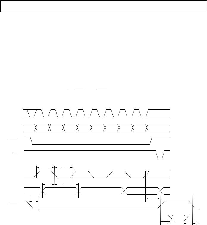
Timing Characteristics
Timing |
|
|
|
|
|
Symbol |
Description |
Min |
Typ |
Max |
Units |
|
|
|
|
|
|
tCL |
Input Clock Pulse Width, Low |
200 |
|
|
ns |
tCH |
Input Clock Pulse Width, High |
200 |
|
|
ns |
tDS |
Data Setup Time |
50 |
|
|
ns |
tDH |
Data Hold Time |
75 |
|
|
ns |
tCW |
Positive CLK Edge to End of Write |
100 |
|
|
ns |
tWC |
Write to Clock Setup Time |
50 |
|
|
ns |
tLW |
End of Load Pulse to Next Write |
50 |
|
|
ns |
tWL |
End of Write to Start of Load |
50 |
|
|
ns |
tL |
Load Pulse Width |
250 |
|
|
ns |
tW3 |
Load Pulse Width (3-Wire Mode) |
250 |
|
|
ns |
NOTES
1.An idle HI (CLK-HI) or idle LO (CLK-LO) clock may be used. Data is latched on the negative edge.
2.For SPI or microwire three-wire bus operation, tie LD to WRITE, and use WRITE pulse to drive both pins. (This generates an automatic internal load signal.)
3.If an idle HI clock is used, tCW and tWL are measured from the final negative transition to the idle state.
4.The first data byte selects an address (MSB HI), and subsequent MSB LO states set gain/attenuation levels. Refer to the Address/Data Decoding Truth Table.
5.Data must be sent MSB first.
0
CLK
1
1
DATA |
D7 |
D6 |
D5 |
D4 |
D3 |
D2 |
D1 |
D0 |
0
1
WRITE |
|
|
0 |
|
|
1 |
|
|
LD |
|
|
0 |
|
|
tCH |
|
tCL |
1 |
|
|
CLK |
|
|
0 |
|
|
tDS |
tDH |
|
1 |
|
|
DATA |
D7 |
|
0 |
|
|
MSB |
tCW |
|
tWC |
|
|
1 |
|
|
WRITE |
|
|
0 |
|
|
1 |
|
|
|
|
|
|
tL |
|
|
|
|
||
|
|
|
|
|
|
|
|
|
|||||
LD |
|
|
|
|
|
|
|
|
|
|
|
||
|
|
|
|
|
|
|
|
|
|
||||
0 |
tWL |
|
|
|
|
|
|
|
|
t |
|||
|
|
|
|
|
|||||||||
|
|
|
|
|
|
|
|
|
|
||||
|
|
|
|
|
|
||||||||
|
|
|
|
|
|
|
|
|
|
|
|
LW |
|
Figure 1. Timing Diagrams
REV. 0 |
–3– |

SSM2160/SSM2161
ABSOLUTE MAXIMUM RATINGS1
Supply Voltage
Dual Supply . . . . . . . . . . . . . . . . . . . . . . . . . . . . . . . . . . ±18 V Single . . . . . . . . . . . . . . . . . . . . . . . . . . . . . . . . . . . . . . . +36 V Logic Input Voltage . . . . . . . . . . . . . . . . . . . . . –0.3 V to +5 V Operating Temperature Range . . . . . . . . . . . . . 0°C to +70°C Storage Temperature Range . . . . . . . . . . . . –65°C to +150°C Junction Temperature Range . . . . . . . . . . . . –65°C to +165°C Lead Temperature Range (Soldering, 60 sec) . . . . . . .+300°C
ESD Ratings |
|
|
|
|
|
883 (Human Body) Model |
. . . . . . . . . . . . . . . . . . . . . . 2.5 kV |
||||
PACKAGE THERMAL INFORMATION |
|
|
|||
|
|
|
|
|
|
Package Type3 |
|
uJA |
|
uJC |
Units |
24-Pin Plastic P-DIP |
|
60 |
|
30 |
°C/W |
24-Pin SOIC |
|
71 |
|
23 |
°C/W |
20-Pin Plastic P-DIP |
|
65 |
|
26 |
°C/W |
20-Pin SOIC |
|
84 |
|
24 |
°C/W |
NOTES
1Absolute maximum ratings apply at +25°C unless otherwise noted. 2VS is the total supply span from V+ to V–.
3θJA is specified for the worst case conditions, i.e., for device in socket for P-DIP, packages and for device soldered onto a circuit board for SOIC packages.
ORDERING GUIDE
|
Temperature |
Package |
Package |
Model |
Range |
Description |
Option |
|
|
|
|
SSM2160P |
0°C to +70°C |
24-Lead Plastic DIP |
N-24 |
SSM2160S |
0°C to +70°C |
24-Lead SOL |
R-24 |
SSM2160S-REEL |
0°C to +70°C |
24-Lead SOL |
R-24 |
SSM2161P |
0°C to +70°C |
20-Lead Plastic DIP |
N-20 |
SSM2161S |
0°C to +70°C |
20-Lead SOL |
R-20 |
SSM2161S-REEL |
0°C to +70°C |
20-Lead SOL |
R-20 |
|
|
|
|
PIN CONFIGURATIONS
24-Lead Epoxy DIP and SOIC
|
|
|
|
|
|
|
24 |
|
|
|
V+ |
1 |
|
CH SET |
|||
|
|
|
|
|
|
|
23 |
|
|
AGND |
2 |
|
MSTR OUT |
||||
|
VREF |
|
|
22 |
|
|||
|
3 |
|
MSTR SET |
|||||
|
|
|
|
|
|
|
|
|
VOUT1 |
4 |
|
21 |
VOUT2 |
||||
|
|
|
|
|
|
|
|
|
|
VIN1 |
5 |
SSM2160 |
20 |
VIN2 |
|||
|
|
|
|
|
|
|
|
|
VOUT3 |
6 |
TOP VIEW |
19 |
VOUT4 |
||||
|
|
|
|
|
|
|
|
|
|
VIN3 |
7 |
(Not to Scale) |
18 |
VIN4 |
|||
|
|
|
|
|
|
|
|
|
VOUT5 |
8 |
|
17 |
VOUT6 |
||||
|
|
|
|
|
|
|
|
|
|
VIN5 |
9 |
|
16 |
VIN6 |
|||
|
|
|
|
|
|
|
|
|
|
WRITE |
|
|
10 |
|
15 |
DATA |
|
|
|
|
|
|
|
14 |
|
|
|
|
LD |
|
11 |
|
CLK |
||
|
|
|
|
|
|
|
|
|
|
|
V– |
12 |
|
13 |
DGND |
||
|
|
|
|
|
|
|
|
|
20-Lead Epoxy DIP and SOIC
V+ |
|
|
|
|
1 |
|
20 |
CH SET |
|
AGND |
|
|
|
|
2 |
|
19 |
MSTR OUT |
|
VREF |
|
|
|
|
3 |
|
18 |
MSTR SET |
|
VOUT1 |
|
|
|
|
4 |
|
17 |
VOUT2 |
|
VIN1 |
|
|
|
|
5 |
SSM2161 |
16 |
VIN2 |
|
VOUT3 |
|
TOP VIEW |
|
|
6 |
15 |
VOUT4 |
||
VIN3 |
|
(Not to Scale) |
|
VIN4 |
7 |
|
14 |
||
|
|
|
|
DATA |
WRITE |
8 |
|
13 |
|
|
|
|
|
CLK |
LD |
9 |
|
12 |
|
V– |
|
|
|
DGND |
10 |
|
11 |
||
|
|
|
|
|
–4– |
REV. 0 |
|
|
|
|
|
|
|
|
|
|
|
|
|
|
SSM2160/SSM2161 |
|
|
|
|
|
|
|
|
|
|
|
|
|
|
|
|
|
|
|
|
|
PIN DESCRIPTIONS |
||||||||
|
|
|
|
|
|
|
|
|
|
|
|
|
|
|
SSM2160 |
SSM2161 |
|
|
|
|
|
|
|
|
|
|
|
|
|
Pin No. |
Pin No. |
|
Name |
Function |
||||||||||
|
|
|
|
|
|
|
|
|
|
|
|
|
|
|
1 |
1 |
|
V+ |
V+ is the positive power supply pin. Refer to the Power Supply Connections section for more |
||||||||||
|
|
|
|
|
|
information. |
||||||||
2 |
2 |
|
AGND |
AGND is the internal ground reference for the audio circuitry. When operating the SSM2160 |
||||||||||
|
|
|
|
|
|
from dual supplies, AGND should be connected to ground. When operating from a single |
||||||||
|
|
|
|
|
|
supply, AGND should be connected to VREF, the internally generated voltage reference. AGND |
||||||||
|
|
|
|
|
|
may also be connected to an external reference. Refer to the Power Supply Connections section |
||||||||
|
|
|
|
|
|
for more details. |
||||||||
3 |
3 |
|
VREF |
VREF is the internally generated ground reference for the audio circuitry obtained from a buffered |
||||||||||
|
|
|
|
|
|
divider between V+ and V–. In a dual-supply application with the AGND pin connected to |
||||||||
|
|
|
|
|
|
ground, VREF should be left floating. In a single supply application, VREF should be connected to |
||||||||
|
|
|
|
|
|
AGND. Refer to the Power Supply Connections section for more details. |
||||||||
4 |
4 |
|
CH1 OUT |
Audio Output from Channel 1. |
||||||||||
5 |
5 |
|
CH1 IN |
Audio Input to Channel 1. |
||||||||||
6 |
6 |
|
CH3 OUT |
Audio Output from Channel 3. |
||||||||||
7 |
7 |
|
CH3 IN |
Audio Input to Channel 3. |
||||||||||
8 |
– |
|
CH5 OUT |
Audio Output from Channel 5. |
||||||||||
9 |
– |
|
CH5 IN |
Audio Input to Channel 5. |
||||||||||
10 |
8 |
|
|
|
|
A logic LOW voltage enables the SSM2160 to receive information at the DATA input (Pin 15). |
||||||||
WRITE |
||||||||||||||
|
|
|
|
|
|
A logic HIGH applied to |
WRITE |
retains data at their previous settings. See Timing Diagrams. |
||||||
|
|
|
|
|
|
Serves as CHIP SELECT. |
||||||||
11 |
9 |
|
|
|
Loads the information retained by |
|
|
into the SSM2160 at logic LOW. See Timing |
||||||
LD |
WRITE |
|||||||||||||
|
|
|
|
|
|
Diagrams. |
||||||||
12 |
10 |
|
V– |
V– is the negative power supply pin. Connect to ground if using in a single supply application. |
||||||||||
|
|
|
|
|
|
Refer to the Power Supply Connections section for more details. |
||||||||
13 |
11 |
|
DGND |
DGND is the digital ground reference for the SSM2160. This pin should always be connected to |
||||||||||
|
|
|
|
|
|
ground. All digital inputs, including |
|
, |
|
, CLK, and DATA are TTL input compatible; |
||||
|
|
|
|
|
|
WRITE |
LD |
|||||||
|
|
|
|
|
|
drive currents are returned to DGND. |
||||||||
14 |
12 |
|
CLK |
CLK is the clock input. It is positive edge triggered. See Timing Diagrams. |
||||||||||
15 |
13 |
|
DATA |
Channel and Master control information flows MSB first into the DATA pin. Refer to Address/ |
||||||||||
|
|
|
|
|
|
Data Decoding Truth Table, Figure 19, for information on how to control the VCAs. |
||||||||
16 |
– |
|
CH6 IN |
Audio Input to Channel 6. |
||||||||||
17 |
– |
|
CH6 OUT |
Audio Output from Channel 6. |
||||||||||
18 |
14 |
|
CH4 IN |
Audio Input to Channel 4. |
||||||||||
19 |
15 |
|
CH4 OUT |
Audio Output from Channel 4. |
||||||||||
20 |
16 |
|
CH2 IN |
Audio Input to Channel 2. |
||||||||||
21 |
17 |
|
CH2 OUT |
Audio Output from Channel 2. |
||||||||||
22 |
18 |
|
MSTR SET |
MSTR SET is connected to the inverting input of an I-V converting op amp used to generate a |
||||||||||
|
|
|
|
|
|
Master Control voltage from the Master Control DAC current output. A resistor connected |
||||||||
|
|
|
|
|
|
from MSTR OUT to MSTR SET reduces the step size of the Master control. See the Adjusting |
||||||||
|
|
|
|
|
|
Step Sizes section for more details. A 10 μF capacitor should be connected from MSTR OUT to |
||||||||
|
|
|
|
|
|
MSTR SET to eliminate the zipper noise in the Master control. |
||||||||
23 |
19 |
|
MSTR OUT |
MSTR OUT is connected to the output of the I-V converting op amp. See MSTR SET |
||||||||||
|
|
|
|
|
|
description. |
||||||||
24 |
20 |
|
CH SET |
The step size of the Channel Control can be increased by connecting a resistor from CH SET to |
||||||||||
|
|
|
|
|
|
V+. No connection to CH SET is required if the default value of 1 dB per step is desired. Mini- |
||||||||
|
|
|
|
|
|
mum of 10 Ω external resistor. See the Adjusting Step Sizes section for more details. |
||||||||
REV. 0 |
–5– |
Loading...