


OP193FS-REEL
Table of contents
 Loading...
Analog Devices OP193FS-REEL, OP193ES, OP293ES, OP493FS, OP493ES-REEL Datasheet
...
Precision, Micropower
NC = NO CONNECT
1
2
3
4
8
7
6
5
OUT A
V+
NULL
NC
NULL
–IN A
+IN A
V–
OP193
OP193
OUT A
V+
NULL
NCNULL
–IN A
+IN A
V–
14
13
12
11
10
9
8
1
2
3
4
5
6
7
OP493
OUT A
–IN A
+IN A
V+
+IN B
–IN B
OUT B
OUT D
–IN D
+IN D
V–
+IN C
–IN C
OUT C
OP493
OUT D
–IN D
+IN D
V–
+IN C
–IN C
OUT C
NC
OUT A
–IN A
+IN A
V+
+IN B
–IN B
OUT B
NC
NC = NO CONNECT
a
FEATURES
Operates from +1.7 V to ⴞ18 V
Low Supply Current: 15 A/Amplifier
Low Offset Voltage: 75 V
Outputs Sink and Source: ⴞ8 mA
No Phase Reversal
Single- or Dual-Supply Operation
High Open-Loop Gain: 600 V/mV
Unity-Gain Stable
APPLICATIONS
Digital Scales
Strain Gages
Portable Medical Equipment
Battery-Powered Instrumentation
Temperature Transducer Amplifier
GENERAL DESCRIPTION
The OP193 family of single-supply operational amplifiers features a combination of high precision, low supply current and
the ability to operate at low voltages. For high performance in
single-supply systems the input and output ranges include
ground, and the outputs swing from the negative rail to within
600 mV of the positive supply. For low voltage operation the
OP193 family can operate down to 1.7 volts or ±0.85 volts.
The combination of high accuracy and low power operation
make the OP193 family useful for battery-powered equipment.
Its low current drain and low voltage operation allow it to
continue performing long after other amplifiers have ceased
functioning either because of battery drain or headroom.
The OP193 family is specified for single +2 volt through dual
±15 volt operation over the HOT (–40°C to +125°C) temperature
range. They are available in plastic DIPs, plus SOIC surfacemount packages.
Operational Amplifiers
OP193/OP293/OP493
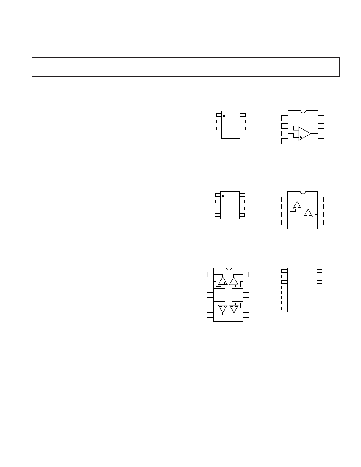
PIN CONFIGURATIONS
8-Lead SO
(S Suffix)
8-Lead SO
(S Suffix)
OUT A
–IN A
OP293
+IN A
V–
14-Lead Epoxy DIP
(P Suffix)
V+
OUT B
–IN B
+IN B
*
8-Lead Epoxy DIP
(P Suffix)
8-Lead Epoxy DIP
(P Suffix)
1
OUT A
–IN A
+IN A
V–
OP293
2
3
4
16-Lead Wide Body SOL
(S Suffix)
8
7
6
5
V+
OUT B
–IN B
+IN B
REV. B
Information furnished by Analog Devices is believed to be accurate and
reliable. However, no responsibility is assumed by Analog Devices for its
use, nor for any infringements of patents or other rights of third parties that
may result from its use. No license is granted by implication or otherwise
under any patent or patent rights of Analog Devices.
One Technology Way, P.O. Box 9106, Norwood, MA 02062-9106, U.S.A.
Tel: 781/329-4700www.analog.com
Fax: 781/326-8703 © Analog Devices, Inc., 2002

OP193/OP293/OP493–SPECIFICATIONS
ELECTRICAL SPECIFICATIONS
(@ VS = ⴞ15.0 V, TA = 25ⴗC unless otherwise noted)
“E” Grade “F” Grade
Parameter Symbol Conditions Min Typ Max Min Typ Max Unit
INPUT CHARACTERISTICS
Offset Voltage V
OS
OP193 75 150 µV
OP193, –40°C ≤ T
≤ +125°C 175 250 µV
A
OP293 100 250 µV
OP293, –40°C ≤ T
≤ +125°C 200 350 µV
A
OP493 125 275 µV
OP493, –40°C ≤ T
Input Bias Current I
B
V
= 0 V,
CM
–40°C ≤ T
Input Offset Current I
OS
VCM = 0 V,
–40°C ≤ T
Input Voltage Range V
CM
Common-Mode Rejection CMRR –14.9 ≤ V
≤ +125°C1520nA
A
≤ +125°C24nA
A
CM
≤ +125°C 225 375 µV
A
–14.9 +13.5 –14.9 +13.5 V
≤ +14 V 100 116 97 116 dB
–14.9 ≤ VCM ≤ +14 V,
Large Signal Voltage Gain A
VO
–40°C ≤ T
RL = 100 kΩ,
–10 V ≤ V
≤ +125°C9794dB
A
≤ +10 V 500 500 V/mV
OUT
–40°C ≤ TA ≤ +85°C 300 300 V/mV
Large Signal Voltage Gain A
VO
–40°C ≤ T
RL = 10 kΩ,
–10 V ≤ V
≤ +125°C 300 300 V/mV
A
≤ +10 V 350 350 V/mV
OUT
–40°C ≤ TA ≤ +85°C 200 200 V/mV
Large Signal Voltage Gain A
VO
–40°C ≤ T
RL = 2 kΩ,
–10 V ≤ V
≤ +125°C 150 150 V/mV
A
≤ +10 V 200 200 V/mV
OUT
–40°C ≤ TA ≤ +85°C 125 125 V/mV
–40°C ≤ TA ≤ +125°C 100 100 V/mV
Long Term Offset Voltage V
OS
Note 1 150 300 µV
Offset Voltage Drift ∆VOS/∆T Note 2 0.2 1.75 µV/°C
OUTPUT CHARACTERISTICS
Output Voltage Swing High V
OH
IL = 1 mA 14.1 14.2 14.1 14.2 V
I
= 1 mA,
L
–40°C ≤ TA ≤ +125°C 14.0 14.0 V
I
= 5 mA 13.9 14.1 13.9 14.1 V
Output Voltage Swing Low V
OL
L
IL = –1 mA –14.7 –14.6 –14.7 –14.6 V
I
= –1 mA,
L
–40°C ≤ TA ≤ +125°C –14.4 –14.4 V
I
= –5 mA +14.2 –14.1 +14.2 –14.1 V
Short Circuit Current I
SC
L
±25 ±25 mA
POWER SUPPLY
Power Supply Rejection Ratio PSRR V
= ±1.5 V to ± 18 V 100 120 97 120 dB
S
V
= ±1.5 V to ± 18 V,
S
–40°C ≤ TA ≤ +125°C9794dB
Supply Current/Amplifier I
SY
–40°C ≤ TA ≤ +125°C, RL = ∞
V
= 0 V, VS = ±18 V 30 30 µA
OUT
NOISE PERFORMANCE
Voltage Noise Density e
Current Noise Density i
n
n
f = 1 kHz 65 65 nV/√Hz
f = 1 kHz 0.05 0.05 pA/√Hz
Voltage Noise en p-p 0.1 Hz to 10 Hz 3 3 µV p-p
DYNAMIC PERFORMANCE
Slew Rate SR R
= 2 kΩ 15 15 V/ms
L
Gain Bandwidth Product GBP 35 35 kHz
Channel Separation V
= 10 V p-p,
OUT
RL = 2 kΩ, f = 1 kHz 120 120 dB
NOTES
1
Long term offset voltage is guaranteed by a 1000 hour life test performed on three independent lots at 125 °C, with an LTPD of 1.3.
2
Offset voltage drift is the average of the –40°C to +25°C delta and the +25°C to +125°C delta.
Specifications subject to change without notice.
–2–
REV. B

OP193/OP293/OP493
ELECTRICAL SPECIFICATIONS
(@ VS = 5.0 V, VCM = 0.1 V, TA = 25ⴗC unless otherwise noted)
“E” Grade “F” Grade
Parameter Symbol Conditions Min Typ Max Min Typ Max Unit
INPUT CHARACTERISTICS
Offset Voltage V
OS
OP193 75 150 µV
OP193, –40°C ≤ T
≤ +125°C 175 250 µV
A
OP293 100 250 µV
OP293, –40°C ≤ T
≤ +125°C 200 350 µV
A
OP493 125 275 µV
OP493, –40°C ≤ T
Input Bias Current I
Input Offset Current I
Input Voltage Range V
B
OS
CM
–40°C ≤ TA ≤ +125°C1520nA
–40°C ≤ TA ≤ +125°C24nA
Common-Mode Rejection CMRR 0.1 ≤ V
≤ 4 V 100 116 96 116 dB
CM
≤ +125°C 225 375 µV
A
0404V
0.1 ≤ VCM ≤ 4 V,
Large Signal Voltage Gain A
VO
–40°C ≤ T
RL = 100 kΩ,
0.03 ≤ V
≤ +125°C92 92 dB
A
≤ 4.0 V 200 200 V/mV
OUT
–40°C ≤ TA ≤ +85°C 125 125 V/mV
Large Signal Voltage Gain A
VO
–40°C ≤ T
RL = 10 kΩ,
0.03 ≤ V
≤ +125°C 130 130 V/mV
A
≤ 4.0 V 75 75 V/mV
OUT
–40°C ≤ TA ≤ +85°C 50 50 V/mV
Long Term Offset Voltage V
OS
–40°C ≤ T
Note 1 150 300 µV
≤ +125°C 70 70 V/mV
A
Offset Voltage Drift ∆VOS/∆T Note 2 0.2 1.25 µV/°C
OUTPUT CHARACTERISTICS
Output Voltage Swing High V
OH
IL = 100 µA 4.4 4.4 V
I
= 1 mA 4.1 4.4 4.1 4.4 V
L
IL = 1 mA,
–40°C ≤ T
≤ +125°C 4.0 4.0 V
A
IL = 5 mA 4.0 4.4 4.0 4.4 V
Output Voltage Swing Low V
OL
IL = –100 µA 140 160 140 160 mV
IL = –100 µA,
–40°C ≤ T
≤ +125°C 220 220 mV
A
No Load 5 5 mV
I
= –1 mA 280 400 280 400 mV
L
IL = –1 mA,
–40°C ≤ T
≤ +125°C 500 500 mV
A
IL = –5 mA 700 900 700 900 mV
Short Circuit Current I
SC
±8 ±8mA
POWER SUPPLY
Power Supply Rejection Ratio PSRR V
= ±1.7 V to ± 6.0 V 100 120 97 120 dB
S
VS = ±1.5 V to ± 18 V,
Supply Current/Amplifier I
–40°C ≤ T
SY
VCM = 2.5 V, RL = ∞ 14.5 14.5 µA
≤ +125°C94 90 dB
A
NOISE PERFORMANCE
Voltage Noise Density e
Current Noise Density i
n
n
f = 1 kHz 65 65 nV/√Hz
f = 1 kHz 0.05 0.05 pA/√Hz
Voltage Noise en p-p 0.1 Hz to 10 Hz 3 3 µV p-p
DYNAMIC PERFORMANCE
Slew Rate SR R
= 2 kΩ 12 12 V/ms
L
Gain Bandwidth Product GBP 35 35 kHz
NOTES
1
Long term offset voltage is guaranteed by a 1000 hour life test performed on three independent lots at 125 °C, with an LTPD of 1.3.
2
Offset voltage drift is the average of the –40°C to +25°C delta and the +25°C to +125°C delta.
Specifications subject to change without notice.
REV. B
–3–

OP193/OP293/OP493
ELECTRICAL SPECIFICATIONS
(@ VS = 3.0 V, VCM = 0.1 V, TA = 25ⴗC unless otherwise noted)
“E” Grade “F” Grade
Parameter Symbol Conditions Min Typ Max Min Typ Max Unit
INPUT CHARACTERISTICS
Offset Voltage V
OS
OP193 75 150 µV
OP193, –40°C ≤ T
≤ +125°C 175 250 µV
A
OP293 100 250 µV
OP293, –40°C ≤ T
≤ +125°C 200 350 µV
A
OP493 125 275 µV
OP493, –40°C ≤ T
Input Bias Current I
Input Offset Current I
Input Voltage Range V
B
OS
CM
–40°C ≤ TA ≤ +125°C1520nA
–40°C ≤ TA ≤ +125°C24nA
Common-Mode Rejection CMRR 0.1 ≤ V
≤ 2 V 97 116 94 116 dB
CM
≤ +125°C 225 375 µV
A
0202V
0.1 ≤ VCM ≤ 2 V,
Large Signal Voltage Gain A
VO
–40°C ≤ T
RL = 100 kΩ, 0.03 ≤ V
–40°C ≤ T
≤ +125°C9087dB
A
≤ +85°C 75 75 V/mV
A
≤ 2 V 100 100 V/mV
OUT
–40°C ≤ TA ≤ +125°C 100 100 V/mV
Long Term Offset Voltage V
OS
Note 1 150 300 µV
Offset Voltage Drift ∆VOS/∆T Note 2 0.2 1.25 µV/°C
OUTPUT CHARACTERISTICS
Output Voltage Swing High V
OH
IL = 1 mA 2.1 2.14 2.1 2.14 V
IL = 1 mA,
–40°C ≤ T
≤ +125°C 1.9 1.9 V
A
IL = 5 mA 1.9 2.1 1.9 2.1 V
Output Voltage Swing Low V
OL
IL = –1 mA 280 400 280 400 mV
IL = –1 mA
–40°C ≤ T
≤ +125°C 500 500 mV
A
IL = –5 mA 700 900 700 900 mV
Short Circuit Current I
SC
±8 ±8mA
POWER SUPPLY
Power Supply Rejection Ratio PSRR V
= +1.7 V to +6 V, 100 97
S
–40°C ≤ TA ≤ +125°C9490dB
Supply Current/Amplifier I
SY
VCM = 1.5 V, RL = ∞ 14.5 22 14.5 22 µA
–40°C ≤ TA ≤ +125°C2222µA
Supply Voltage Range V
S
+2 ±18 +2 ± 18 V
NOISE PERFORMANCE
Voltage Noise Density e
Current Noise Density i
n
n
f = 1 kHz 65 65 nV/√Hz
f = 1 kHz 0.05 0.05 pA/√Hz
Voltage Noise en p-p 0.1 Hz to 10 Hz 3 3 µV p-p
DYNAMIC PERFORMANCE
Slew Rate SR R
= 2 kΩ 10 10 V/ms
L
Gain Bandwidth Product GBP 25 25 kHz
Channel Separation V
= 10 V p-p,
OUT
RL = 2 kΩ, f = 1 kHz 120 120 dB
NOTES
1
Long term offset voltage is guaranteed by a 1000 hour life test performed on three independent lots at 125 °C, with an LTPD of 1.3.
2
Offset voltage drift is the average of the –40°C to +25°C delta and the +25°C to +125°C delta.
Specifications subject to change without notice.
–4–
REV. B

OP193/OP293/OP493
ELECTRICAL SPECIFICATIONS
(@ VS = 2.0 V, VCM = 0.1 V, TA = 25ⴗC unless otherwise noted)
“E” Grade “F” Grade
Parameter Symbol Conditions Min Typ Max Min Typ Max Unit
INPUT CHARACTERISTICS
Offset Voltage V
OS
OP193 75 150 µV
OP193, –40°C ≤ T
≤ +125°C 175 250 µV
A
OP293 100 250 µV
OP293, –40°C ≤ T
≤ +125°C 175 350 µV
A
OP493 125 275 µV
Input Bias Current I
Input Offset Current I
Input Voltage Range V
Large Signal Voltage Gain A
B
OS
CM
VO
OP493, –40°C ≤ T
–40°C ≤ TA ≤ +125°C1520nA
–40°C ≤ TA ≤ +125°C24nA
RL = 100 kΩ, 0.03 ≤ V
≤ +125°C 225 375 µV
A
0101V
≤ 1 V 60 60 V/mV
OUT
–40°C ≤ TA ≤ +125°C 70 70 V/mV
Long Term Offset Voltage V
OS
Note 1 150 300 µV
POWER SUPPLY
Power Supply Rejection Ratio PSRR V
Supply Current/Amplifier I
Supply Voltage Range V
SY
S
= 1.7 V to 6 V, 100 97
S
–40°C ≤ T
≤ +125°C9490dB
A
VCM = 1.0 V, RL = ∞ 13.2 20 13.2 20 µA
–40°C ≤ T
≤ +125°C2525µA
A
+2 ±18 +2 ± 18 V
NOISE PERFORMANCE
Voltage Noise Density e
Current Noise Density i
n
n
f = 1 kHz 65 65 nV/√Hz
f = 1 kHz 0.05 0.05 pA/√Hz
Voltage Noise en p-p 0.1 Hz to 10 Hz 3 3 µV p-p
DYNAMIC PERFORMANCE
Slew Rate SR R
= 2 kΩ 10 10 V/ms
L
Gain Bandwidth Product GBP 25 25 kHz
Specifications subject to change without notice.
REV. B
–5–
Loading...