


 Loading...
a |
Trimless |
Voltage Controlled Amplifiers |
|
|
SSM2018T/SSM2118T* |
FEATURES
117 dB Dynamic Range
0.006% Typical THD+N (@ 1 kHz, Unity Gain)
140 dB Gain Range
No External Trimming Required
Differential Inputs
Complementary Gain Outputs
Buffered Control Port
I–V Converter On-Chip (SSM2018T)
Differential Current Outputs (SSM2118T)
Low External Parts Count
Low Cost
GENERAL DESCRIPTION
The SSM2018T and SSM2118T represent continuing evolution of the Frey Operational Voltage Controlled Element (OVCE) topology that permits flexibility in the design of high performance volume control systems. Voltage (SSM2018T) and differential current (SSM2118T) output versions are offered, both laser-trimmed for gain core symmetry and offset. As a result, the SSM2018T is the first professional audio quality VCA to offer trimless operation. The SSM2118T is ideal for low noise summing in large VCA based systems.
Due to careful gain core layout, the SSM2018T/SSM2118T combine the low noise of Class AB topologies with the low distortion of Class A circuits to offer an unprecedented level of sonic transparency. Additional features include differential inputs, a 140 dB gain range, and a high impedance control port. The SSM2018T provides an internal current-to-voltage converter; thus no external active components are required. The SSM2118T has fully differential current outputs that permit high noise-immunity summing of multiple channels.
Both devices are offered in 16-pin plastic DIP and SOIC packages and guaranteed for operation over the extended industrial temperature range of –40°C to +85°C.
*Protected by U.S. Patent Nos. 4,471,320 and 4,560,947.
REV. A
Information furnished by Analog Devices is believed to be accurate and reliable. However, no responsibility is assumed by Analog Devices for its use, nor for any infringements of patents or other rights of third parties which may result from its use. No license is granted by implication or otherwise under any patent or patent rights of Analog Devices.
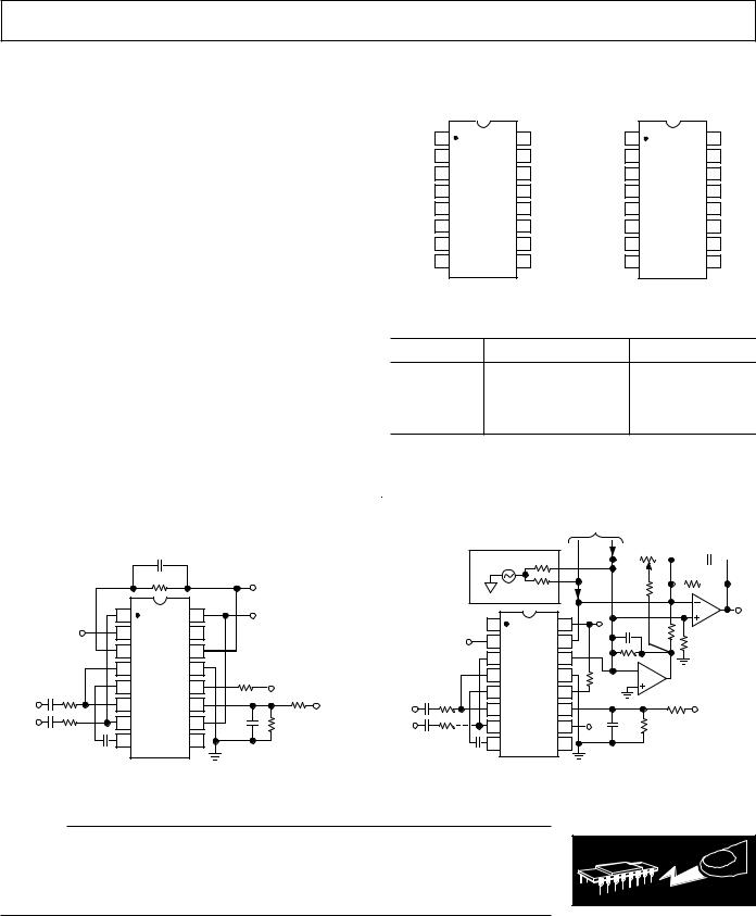
FUNCTIONAL BLOCK DIAGRAMS
VC |
|
SSM-2018T |
|
|
|
|
G |
VG |
+IN |
GAIN |
–IG |
|
CORE |
|
–IN |
|
|
|
1–G |
V1–G |
|
|
–I1–G |
VC |
|
SSM-2118T |
|
|
|
|
|
+IG |
|
G |
|
|
|
–IG |
+IN |
GAIN |
|
|
|
|
|
CORE |
|
–IN |
|
|
|
1–G |
V1–G |
|
|
–I1–G |
One Technology Way, P.O. Box 9106, Norwood. MA 02062-9106, U.S.A. Tel: 617/329-4700 Fax: 617/326-8703
SSM1018T/SSM2118T–SPECIFICATIONS
ELECTRICAL SPECIFICATIONS [VS = ±15 V, AV = 0 dB, RL = 100 kΩ, f = 1 kHz, 0 dBu = 0.775 V rms, simple VCA application circuit with 18 kΩ resistors, –VIN floating, and Class AB gain core bias (RB = 150 kΩ), –40°C < TA < +85°C, unless otherwise noted. Typical specifications apply at TA = +25°C.]
Parameter |
Conditions |
Min |
Typ |
Max |
Units |
|
|
|
|
|
|
AUDIO PERFORMANCE1 |
|
|
|
|
|
Noise |
VIN = GND, 20 kHz Bandwidth |
|
–95 |
–93 |
dBu |
Headroom |
Clip Point = 1% THD+N |
|
+22 |
|
dBu |
Total Harmonic Distortion plus Noise |
2nd and 3rd Harmonics Only (+25°C to +85°C) |
|
|
|
|
|
AV = 0 dB, VIN = +10 dBu |
|
0.006 |
0.025 |
% |
|
AV = +20 dB, VIN = –10 dBu |
|
0.013 |
0.04 |
% |
|
AV = –20 dB, VIN = +10 dBu2 |
|
0.013 |
0.04 |
% |
INPUT AMPLIFIER |
|
|
|
|
μA |
Bias Current |
VCM = 0 V |
|
0.25 |
1 |
|
Offset Voltage |
VCM = 0 V |
|
1 |
15 |
mV |
Offset Current |
VCM = 0 V |
|
10 |
100 |
nA |
Input Impedance |
|
|
4 |
|
MΩ |
Common-Mode Range |
|
|
±13 |
|
V |
Gain Bandwidth |
VCA Configuration |
|
0.7 |
|
MHz |
|
VCP Configuration |
|
14 |
|
MHz |
Slew Rate |
|
|
5 |
|
V/μs |
OUTPUT AMPLIFIER (SSM2018T) |
|
|
|
|
|
Offset Voltage |
VIN = 0 V, VC = +4 V |
|
1.0 |
15 |
mV |
Output Voltage Swing |
IOUT = 1.5 mA |
|
|
|
|
|
Positive |
+10 |
+13 |
|
V |
|
Negative |
–10 |
–14 |
|
V |
Minimum Load Resistance |
For Full Output Swing |
|
9 |
|
kΩ |
CONTROL PORT |
|
|
|
|
μA |
Bias Current |
|
|
0.36 |
1 |
|
Input Impedance |
|
|
1 |
|
MΩ |
Gain Constant |
Device Powered in Socket > 60 sec |
|
–30 |
|
mV/dB |
Gain Constant Temperature Coefficient |
|
|
–3500 |
±4 |
ppm/°C |
Control Feedthrough |
0 dB to –40 dB Gain Range |
|
±1 |
mV |
|
Maximum Attenuation |
VC = +4 V |
|
100 |
|
dB |
POWER SUPPLIES |
|
±5 |
|
±18 |
|
Supply Voltage Range |
|
|
V |
||
Supply Current |
|
|
11 |
15 |
mA |
Power Supply Rejection Ratio |
|
|
80 |
|
dB |
|
|
|
|
|
|
NOTES
1SSM2118T tested and characterized using OP275 as current-to-voltage converter, see figure next page. 2Guaranteed by characterization data and testing at AV = 0 dB.
Specifications subject to change without notice.
–2– |
REV. A |
SSM2018T/SSM2118T
ABSOLUTE MAXIMUM RATINGS1
Supply Voltage
Dual Supply . . . . . . . . . . . . . . . . . . . . . . . . . . . . . . . . .±18 V
Input Voltage . . . . . . . . . . . . . . . . . . . . . . . . . . . . . . . . . . . ±VS Operating Temperature Range . . . . . . . . . . . . .–40°C to +85°C
Storage Temperature . . . . . . . . . . . . . . . . . . . –65°C to +150°C Junction Temperature (TJ) . . . . . . . . . . . . . . . . . . . . . +150°C Lead Temperature (Soldering, 60 sec) . . . . . . . . . . . . . +300°C
THERMAL CHARACTERISTICS
Thermal Resistance2
16-Pin Plastic DIP
θJA . . . . . . . . . . . . . . . . . . . . . . . . . . . . . . . . . . . . . . 76°C/W θJC . . . . . . . . . . . . . . . . . . . . . . . . . . . . . . . . . . . . . . 33°C/W
16-Pin SOIC
θJA . . . . . . . . . . . . . . . . . . . . . . . . . . . . . . . . . . . . . . 92°C/W θJC . . . . . . . . . . . . . . . . . . . . . . . . . . . . . . . . . . . . . . 27°C/W
TRANSISTOR COUNT
Number of Transistors
SSM2018T . . . . . . . . . . . . . . . . . . . . . . . . . . . . . . . . . . 125 SSM2118T . . . . . . . . . . . . . . . . . . . . . . . . . . . . . . . . . . 108
ESD RATINGS |
|
883 (Human Body) Model . . . . . . . . . . . . . . . . . . . . . . . |
500 V |
EIAJ Model . . . . . . . . . . . . . . . . . . . . . . . . . . . . . . . . . . . |
100 V |
1Stresses above those listed under “Absolute Maximum Ratings” may cause permanent damage to the device. This is a stress rating only and functional operation of the device at these or any other conditions above those indicated in the operation section of this specification is not implied. Exposure to absolute maximum rating conditions for extended periods may affect device reliability.
2θJA is specified for worst-case conditions, i.e., θJA is specified for device in socket for P-DIP and device soldered in circuit board for SOIC package.
50pF
18k
|
|
|
|
|
VOUT |
|
|
1 |
16 |
|
V– |
|
V+ |
2 |
15 |
|
|
|
|
3 |
14 |
|
|
|
|
4 |
SSM2018T 13 |
150k |
|
1 F |
|
|
|
|
|
18k |
5 |
12 |
|
V+ |
|
|
|
|
|
||
VIN+ |
|
6 |
11 |
|
VCONTROL |
VIN– |
|
7 |
10 |
1 F |
3k |
|
1k |
||||
1 F |
18k |
8 |
9 |
|
|
|
|
|
|
||
|
|
47pF |
|
|
|
SSM2018T Typical Application Circuit
|
|
|
PIN CONFIGURATIONS |
|
|
|
||||||
16-Lead Plastic DIP |
16-Lead Plastic DIP |
|||||||||||
|
|
and SOL |
|
|
|
|
and SOL |
|
|
|
||
+I1–G |
1 |
|
|
16 |
V1–G |
BAL |
1 |
|
|
16 |
V+ |
|
V+ |
2 |
|
|
15 |
BAL |
V1–G |
2 |
|
|
15 |
–IG |
|
–IG |
3 |
|
|
14 |
VG |
+I1–G |
3 |
|
|
14 |
+IG |
|
–I1–G |
4 SSM2018T 13 |
GND |
–I1–G |
4 |
SSM2118T |
|
13 |
GND |
||||
COMP 1 |
5 |
TOP VIEW |
12 |
MODE |
COMP 1 |
5 |
TOP VIEW |
|
12 |
MODE |
||
(Not to Scale) |
(Not to Scale) |
|||||||||||
|
|
|
|
|
|
|
|
|||||
+IN |
6 |
|
|
11 |
VC |
+IN |
6 |
|
|
11 |
VC |
|
–IN |
7 |
|
|
10 |
V– |
–IN |
7 |
|
|
10 |
V– |
|
COMP 2 |
8 |
|
|
9 |
COMP 3 |
COMP 2 |
8 |
|
|
9 |
COMP 3 |
|
|
|
|
|
ORDERING GUIDE |
|
|
|
|
||||
Model |
|
|
Temperature Range |
|
Package Option* |
|||||||
SSM2018TP |
–40°C to +85°C |
|
N-16 |
|
|
|
||||||
SSM2018TS |
–40°C to +85°C |
|
R-16 |
|
|
|
||||||
SSM2118TP |
–40°C to +85°C |
|
N-16 |
|
|
|
||||||
SSM2118TS |
–40°C to +85°C |
|
R-16 |
|
|
|
||||||
*N = Plastic DIP; R = SOL. |
|
|
|
|
|
|
|
|||||
|
|
|
|
|
|
FROM |
|
|
|
|
|
|
|
|
|
|
|
|
ADDITIONAL |
|
|
|
|
||
|
|
|
|
|
|
SSM2118Ts |
|
GLOBAL |
|
|
|
|
|
|
|
|
|
|
|
|
SYMMETRY |
|
|
|
|
|
|
|
|
|
|
|
|
TRIM |
50pF |
|
||
|
|
|
OPTIONAL |
47k |
|
|
500k |
|
||||
|
|
|
|
|
|
|
|
|
||||
|
|
|
TRIM |
|
|
|
|
18k |
|
|
|
|
|
|
|
|
|
|
|
|
|
|
|
||
|
|
|
|
|
47k |
|
470k |
|
|
|
||
|
|
|
|
|
|
|
|
|
|
|
||
|
|
|
|
|
|
V+ |
|
A2 |
VOUT |
|||
|
|
|
1 |
|
16 |
50pF* |
|
|
||||
|
|
|
|
|
|
|
||||||
|
V– |
2 |
|
15 |
|
|
10k |
|
|
|
||
|
|
|
|
18k |
|
|||||||
|
|
|
|
|
|
|
|
|
||||
|
|
|
3 |
|
14 |
10k |
|
|
|
|
||
|
|
|
4 SSM2118T 13 |
|
|
|
|
|||||
|
|
|
150k |
|
A1 |
|
|
|
||||
|
|
|
|
|
|
|
|
|
|
|||
1 F 18k |
|
5 |
|
12 |
|
|
A1, A2: OP275 |
|||||
|
|
|
|
|
|
|
|
|||||
|
|
|
|
|
|
|
|
|
|
|||
VIN+ |
|
|
6 |
|
11 |
V– |
1 F |
3k |
|
VCONTROL |
||
VIN– |
|
|
|
|
|
|
|
|
||||
|
|
7 |
|
10 |
|
1k |
|
|
|
|||
1 F 18k |
|
8 |
|
9 |
|
|
|
|
|
|
||
|
|
|
|
|
|
|
|
|
|
|||
|
|
|
47pF |
|
|
*FOR MORE THAN 2 SSM2118Ts |
||||||
SSM2118T Typical Application Circuit
CAUTION
ESD (electrostatic discharge) sensitive device. Electrostatic charges as high as 4000 V readily accumulate on the human body and test equipment and can discharge without detection. Although the SSM2018T/SSM2118T features proprietary ESD protection circuitry, permanent damage may occur on devices subjected to high energy electrostatic discharges. Therefore, proper ESD precautions are recommended to avoid performance degradation or loss of functionality.
WARNING!
ESD SENSITIVE DEVICE
REV. A |
–3– |

SSM2018T/SSM2118T–Typical Characteristics
0.1 |
|
|
|
|
|
|
|
|
|
TA = +25°C |
|
|
|
|
|
|
|
|
VS = ±15V |
|
|
|
|
|
|
|
|
RF = 18kΩ |
|
|
|
AV = +20dB |
|
|
|
+ N – % |
|
|
|
|
|
|
||
|
|
|
|
|
|
|
|
|
|
|
|
|
|
|
|
|
|
0.010 |
|
|
|
AV = –20dB |
|
|
|
|
THD |
|
|
|
|
|
|
||
|
|
|
|
|
|
|
|
|
|
|
|
|
|
|
|
||
|
|
|
AV = 0dB |
|
|
|||
0.001 |
100 |
|
|
1k |
10k |
20k |
||
20 |
|
|
||||||
FREQUENCY – Hz
1
TA = +25°C
VS = ±15V
RF = 18kΩ
0.1
THD + N – %
0.010
0.001
10m
0.1 |
1 |
2 |
AMPLITUDE – VRMS
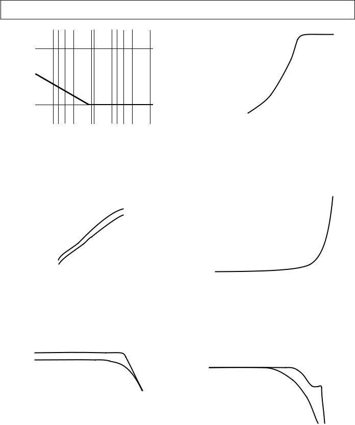
Figure 1. SSM2018T THD + N Frequency (80 kHz Low-Pass Filter, for AV = 0 dB, VIN = 3 V rms; for AV = +20 dB,
VIN = 0.3 V rms; for AV = –20 dB, VIN = 3 V rms)
100
90TA = +25°C AV = 0dB
|
80 |
|
300 UNITS |
|
|
|
|
|
|
|
|
|
|
|
|
|
||
|
|
VIN = 10dBu |
|
|
|
|
|
|
|
|
|
|
|
|
|
|||
|
|
|
|
|
|
|
|
|
|
|
|
|
|
|
|
|||
|
70 |
|
V |
S = ±15V |
|
|
|
|
|
|
|
|
|
|
|
|
|
|
|
|
|
|
|
|
|
|
|
|
|
|
|
|
|
||||
UNITS |
60 |
|
|
|
|
|
|
|
|
|
|
|
|
|
|
|
|
|
50 |
|
|
|
|
|
|
|
|
|
|
|
|
|
|
|
|
|
|
|
|
|
|
|
|
|
|
|
|
|
|
|
|
|
|
|
|
|
|
40 |
|
|
|
|
|
|
|
|
|
|
|
|
|
|
|
|
|
|
30 |
|
|
|
|
|
|
|
|
|
|
|
|
|
|
|
|
|
|
|
|
|
|
|
|
|
|
|
|
|
|
|
|
|
|
|
|
|
|
|
|
|
|
|
|
|
|
|
|
|
|
|
|
|
|
|
|
20 |
|
|
|
|
|
|
|
|
|
|
|
|
|
|
|
|
|
|
|
|
|
|
|
|
|
|
|
|
|
|
|
|
|
|
|
|
|
10 |
|
|
|
|
|
|
|
|
|
|
|
|
|
|
|
|
|
|
|
|
|
|
|
|
|
|
|
|
|
|
|
|
|
|
|
|
|
0 |
|
|
|
|
|
|
|
|
|
|
|
|
|
|
|
|
|
|
|
|
|
|
|
|
|
|
|
|
|
|
|
|
|
|
|
|
|
0.000 |
0.005 |
0.010 |
0.015 |
0.020 |
|
0.025 |
|||||||||||
DISTORTION – %
Figure 2. SSM2018T Distortion Distribution
1
TA = +25°C
RF = 18kΩ
VS = ±15V
0.1
THD + N – %
0.010 |
|
|
|
0.001 |
1 |
10 |
20 |
0.1 |
AMPLITUDE – VRMS
Figure 3. SSM2018T THD + N vs. Amplitude (Gain = 0 dB, fIN = 1 kHz, 80 kHz Low-Pass Filter)
Figure 4. SSM2018T THD + N vs. Amplitude (Gain = +20 dB, fIN =1 kHz, 80 kHz Low-Pass Filter)
1.0
TA = +25°C
VS = ±15V
RF = 18kΩ
0.1
THD + N – %
0.01
0.001 |
|
|
|
|
|
–60 |
–40 |
–20 |
0 |
20 |
40 |
GAIN – dB
Figure 5. SSM2018T THD + N vs. Gain (fIN = 1 kHz;
for –60 dB ≤ AV ≤ –20 dB, VIN = 10 V rms; for 0 dB ≤ AV ≤ +20 dB, VIN = 1 V rms)
0.1
TA = +25°C
RF = 18kΩ
%–
N+ 0.01 THD
0.001
0 |
±3 |
±6 |
±9 |
±12 |
±15 |
±18 |
SUPPLY VOLTAGE – Volts
Figure 6. SSM2018T THD + N vs. Supply Voltage
(AV = 0 dB, VIN = 1 V rms, fIN = 1 kHz, 80 kHz Low-Pass Filter)
–4– |
REV. A |
|
|
|
500 |
|
|
|
|
|
|
|
|
|
|
|
|
|
|
|
|
|
|
|
|
|
|
|
|
|
|
|
|
|
|
|
|
|
|
TA = +25°C |
|
|
|
|
|
|
|
|
|
|
VS = ±15V |
|
|
|
|
|
|
|
|
400 |
|
|
|
|
|
|
|
|
|
nV/√Hz |
300 |
|
|
|
|
|
|
|
|
|
|
|
|
|
|
|
|||
|
|
|
|
|
|
|
|
|||
|
|
DENSITY – |
|
|
|
|
|
|
|
|
|
|
200 |
|
|
|
|
|
|
|
|
|
|
NOISE |
100 |
|
|
|
|
|
|
|
|
|
|
|
|
|
|
|
|
|
|
|
|
|
0 |
|
|
|
|
|
|
|
|
|
|
|
|
|
|
|
|
|
|
|
|
|
10 |
100 |
1k |
10k |
100k |
|||
FREQUENCY – Hz
Figure 7. SSM2018T Noise Density vs. Frequency
|
|
|
|
|
|
|
|
|
|
|
|
|
|
|
|
RF = 18kΩ |
|
|
|
|
|
|
|
|
|
PEAK |
|
TA = +25°C |
|
|
|
|
|
|
|
|
||
– V |
±20 |
|
|
|
|
|
|
|
|
|
|
|
|
|
|
|
|
|
|
RL = ∞Ω |
|
|
|||
|
|
|
|
|
|
|
|
|
|
|||
SWING |
|
|
|
|
|
|
|
|
|
|
||
±15 |
|
|
|
|
|
|
|
|
|
|
|
|
VOLTAGE |
|
|
|
|
|
|
|
|
|
|
|
|
|
|
|
|
|
|
|
|
|
|
|
|
|
±10 |
|
|
|
|
|
|
|
|
RL = 10kΩ |
|
||
|
|
|
|
|
|
|
|
|
|
|||
OUTPUT |
|
|
|
|
|
|
|
|
|
|
|
|
|
|
|
|
|
|
|
|
|
|
|
||
±5 |
|
|
|
|
|
|
|
|
|
|
|
|
|
|
|
|
|
|
|
|
|
|
|
|
|
|
0 |
|
|
|
|
|
|
|
|
|
|
|
|
±5 |
±10 |
±15 |
±20 |
|
|||||||
|
0 |
|
||||||||||
SUPPLY VOLTAGE – Volts
Figure 8. SSM2018T Maximum Output Swing vs. Supply Voltage (THD = 1% max)
|
|
|
|
|
|
|
|
|
|
|
|
|
|
|
|
|
|
|
|
|
RF = |
18kΩ |
|
|
|
|
|
|
|
|
|
||||
PEAK |
±15 |
|
TA = +25°C |
|
|
|
|
|
RL = ∞ |
|
|
|
|
|
|
||
|
VS = ±15V |
|
|
|
|
|
|
|
|
|
|
|
|||||
– V |
|
|
|
|
|
|
|
|
|
|
|
|
|
|
|||
|
|
|
|
|
|
|
|
|
|
|
|
|
|
|
|
|
|
|
|
|
|
|
|
|
|
|
|
|
|
|
|
|
|
|
|
SWING |
±12 |
|
|
|
|
|
|
|
|
|
|
|
|
|
|
|
|
|
|
|
|
|
|
|
|
|
|
|
|
|
|
|
|
||
|
|
|
|
|
|
|
|
|
|
|
|
|
|
|
|
|
|
|
|
|
|
|
|
|
|
|
RL = 10k |
|
|
|
|
|
|||
|
|
|
|
|
|
|
|
|
|
|
|
|
|
|
|||
OUTPUT |
±9 |
|
|
|
|
|
|
|
|
|
|
|
|
|
|
|
|
|
|
|
|
|
|
|
|
|
|
|
|
|
|
|
|
|
|
MAXIMUM |
±6 |
|
|
|
|
|
|
|
|
|
|
|
|
|
|
|
|
|
|
|
|
|
|
|
|
|
|
|
|
|
|
|
|
||
±3 |
|
|
|
|
|
|
|
|
|
|
|
|
|
|
|
|
|
|
|
|
|
|
|
|
|
|
|
|
|
|
|
|
|
||
|
0 |
|
|
|
|
|
|
|
|
|
|
|
|
|
|
|
|
|
|
|
|
|
|
|
|
|
|
|
|
|
|
|
|
|
|
|
1k |
|
|
|
|
|
10k |
|
100k |
||||||||
|
|
|
|
|
|
FREQUENCY – Hz |
|
|
|
|
|||||||
Figure 9. SSM2018T Maximum Output Swing vs. Frequency (THD = 1 % max)
SSM2018T/SSM2118T
|
±15 |
|
|
|
|
|
|
|
|
|
|
|
|
|
|
|
|
|
|
|
|
|
RF |
= 18kΩ |
|
|
|
|
|
|
|
|
|
|
|
|
|
|
|
|
|
|
TA = +25°C |
|
|
|
|
|
|
|
|
|
|
|
|
|
|
||
PEAK |
±12 |
|
VS = ±15V |
|
|
|
|
|
|
|
|
|
|
|
|
|
|
||
– V |
|
|
|
|
|
|
|
|
|
|
|
|
|
|
|
|
|
|
|
OUTPUTSWING |
±6 |
|
|
|
|
|
|
|
|
|
|
|
|
|
|
|
|
|
|
MAXIMUM |
±9 |
|
|
|
|
|
|
|
|
|
|
|
|
|
|
|
|
|
|
±3 |
|
|
|
|
|
|
|
|
|
|
|
|
|
|
|
|
|
|
|
|
|
|
|
|
|
|
|
|
|
|
|
|
|
|
|
|
|
||
|
|
|
|
|
|
|
|
|
|
|
|
|
|
|
|
|
|
|
|
|
0 |
|
|
|
|
|
|
|
|
|
|
|
|
|
|
|
|
|
|
|
|
|
|
|
|
|
|
|
|
|
|
|
|
|
|
|
|
|
|
|
100 |
|
|
|
|
|
1k |
|
|
|
10k |
|
|
100k |
|||||
|
|
|
|
|
|
|
|
LOAD RESISTANCE – Ω |
|
|
|
|
|
||||||
Figure 10. SSM2018T Maximum Output Swing vs. Load Resistance, (THD = 1 % max)
|
100 |
|
|
|
|
|
|
|
|
|
|
|
|
|
|
|
|
|
|
|
|
|
|
|
|
|
|
|
|
|
|
|
|
|
|
|
|
|
|
|
|
|
90 |
|
TA = +25°C |
|
|
|
|
|
|
|
|
|
|
|
|
|
|
|
|
|
|
|
|
|
|||
|
80 |
|
VS = ±15V |
|
|
|
|
|
|
|
|
|
|
mV |
70 |
|
|
|
|
|
|
|
|
|
|
|
|
|
|
|
|
|
|
|
|
|
|
|
|
||
– |
|
|
|
|
|
|
|
|
|
|
|
|
|
OFFSET |
60 |
|
|
|
|
|
|
|
|
|
|
|
|
|
|
|
|
|
|
|
|
|
|
|
|
|
|
OUTPUT |
50 |
|
|
|
|
|
|
|
|
|
|
|
|
|
|
|
|
|
|
|
|
|
|
|
|
||
30 |
|
|
|
|
|
|
|
|
|
|
|
|
|
|
40 |
|
|
|
|
|
|
|
|
|
|
|
|
|
20 |
|
|
|
|
|
|
|
|
|
|
|
|
|
|
|
|
|
|
|
|
|
|
|
|
|
|
|
10 |
|
|
|
|
|
|
|
|
|
|
|
|
|
|
|
|
|
|
|
|
|
|
|
|
|
|
|
0 |
|
|
|
|
|
|
|
|
|
|
|
|
|
|
|
|
|
|
|
|
|
|
|
|
|
|
|
–80 |
–60 |
–40 |
–20 |
0 |
20 |
40 |
||||||
GAIN – dB
Figure 11. SSM2018T Output Offset vs. Gain
|
+10 |
|
|
|
|
|
|
|
|
|
|
|
|
|
|
|
|
|
|
|
|
|
|
|
|
|
|
|
|
|
|
|
|
|
|
|
|
|
|
|
|
|
|
|
|
|
|
|
|
|
|
|
|
|
|
|
|
|
|
|
TA |
= +25°C |
|
|
|
|
|
|
|
|
|
|
|
|
|
|
|
|
|
|
|
|
|
|
||
|
|
|
VS = ±15V |
|
|
|
|
|
|
|
|
|
|
|
|
|
|
|
|
|
|
|
|
|
|
|||
|
+5 |
|
|
|
|
|
|
|
|
|
|
|
|
|
|
|
|
|
|
|
|
|
|
|
|
|
0 |
Degrees |
|
|
|
|
|
|
|
|
|
|
|
|
|
|
|
|
|
|
|
|
|
|
|
|
|
|
|||
dB– |
0 |
|
|
|
|
|
|
|
|
|
|
|
|
|
|
|
|
|
|
|
|
|
|
|
|
|
||
|
|
|
|
|
|
|
|
|
|
|
|
|
|
|
|
|
|
|
|
|
|
|
|
|
|
|
||
|
|
|
|
|
|
|
|
|
|
|
|
|
|
|
|
|
|
|
|
|
|
|
GAIN |
|
|
|
|
|
GAIN |
|
|
|
|
|
|
|
|
|
|
|
|
|
|
|
|
|
|
|
|
|
|
|
|
|
|
|
PHASE– |
|
|
|
|
|
|
|
|
|
|
|
|
|
|
PHASE |
|
|
|
|
|
|
|
|
|
|
||||
|
|
|
|
|
|
|
|
|
|
|
|
|
|
|
|
|
|
|
|
|
|
|
|
|
|
|||
|
–5 |
|
|
|
|
|
|
|
|
|
|
|
|
|
|
|
|
|
|
|
|
|
|
|
|
|
–45 |
|
|
|
|
|
|
|
|
|
|
|
|
|
|
|
|
|
|
|
|
|
|
|
|
|
|
|
|
||
|
–10 |
|
|
|
|
|
|
|
|
|
|
|
|
|
|
|
|
|
|
|
|
|
|
|
|
|
–90 |
|
|
|
|
|
|
|
|
|
|
|
|
|
|
|
|
|
|
|
|
|
|
|
|
|
|
|
|
||
|
–15 |
|
|
|
|
|
|
|
|
|
|
|
|
|
|
|
|
|
|
|
|
|
|
|
|
|
–135 |
|
|
|
|
|
|
|
|
|
|
|
|
|
|
|
|
|
|
|
|
|
|
|
|
|
|
|
|
||
|
100 |
|
|
|
|
|
1k |
|
|
10k |
|
|
|
|
100k |
|
|
|
1M |
|
||||||||
FREQUENCY – Hz
Figure 12. SSM2018T Gain/Phase vs. Frequency
REV. A |
–5– |
Loading...