


SSM2166S
Table of contents
 Loading...
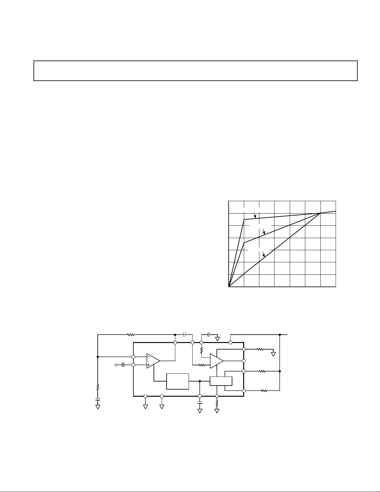
a
SSM2166*
Microphone Preamplifier with
Variable Compression and Noise Gating
Information furnished by Analog Devices is believed to be accurate and
reliable. However, no responsibility is assumed by Analog Devices for its
use, nor for any infringements of patents or other rights of third parties
which may result from its use. No license is granted by implication or
otherwise under any patent or patent rights of Analog Devices.
FEATURES
Complete Microphone Conditioner in a 14-Lead Package
Single +5 V Operation
Adjustable Noise Gate Threshold
Compression Ratio Set by External Resistor
Automatic Limiting Feature—Prevents ADC Overload
Adjustable Release Time
Low Noise and Distortion
Power-Down Feature
20 kHz Bandwidth (ⴞ1 dB)
Low Cost
APPLICATIONS
Microphone Preamplifier/Processor
Computer Sound Cards
Public Address/Paging Systems
Communication Headsets
Telephone Conferencing
Guitar Sustain Effects Generator
Computerized Voice Recognition
Surveillance Systems
Karaoke and DJ Mixers
20 dB; this gain is in addition to the variable gain in other com-
pression settings. The input buffer can also be configured for front-
end gains of 0 dB to 20 dB. A downward expander (noise gate)
prevents amplification of noise or hum. This results in opti-
mized signal levels prior to digitization, thereby eliminating the
need for additional gain or attenuation in the digital domain
that could add noise or impair accuracy of speech recognition
algorithms. The compression ratio and time constants are set
externally. A high degree of flexibility is provided by the VCA
Gain, Rotation Point, and Noise Gate adjustment pins.
The SSM2166 is an ideal companion product for audio codecs
used in computer systems, such as the AD1845 and AD1847.
The device is available in 14-lead SOIC and P-DIP packages,
and guaranteed for operation over the extended industrial tempera-
ture range of –40°C to +85°C. For similar features/performance
in an 8-lead package, please refer to the SSM2165.
INPUT – dBu
–70 0–60 –50 –40 –30 –20 –10
10
OUTPUT – dBu
0
–30
–40
–50
–60
–10
–20
RATIO = 10:1
RATIO = 2:1
RATIO = 1:1
Figure 1. SSM2166 Compression and Gating Characteris-
tics with 10 dB of Fixed Gain (The Gain Adjust Pin Can Be
Used to Vary This Fixed Gain Amount)
REV. A
*Patents pending.
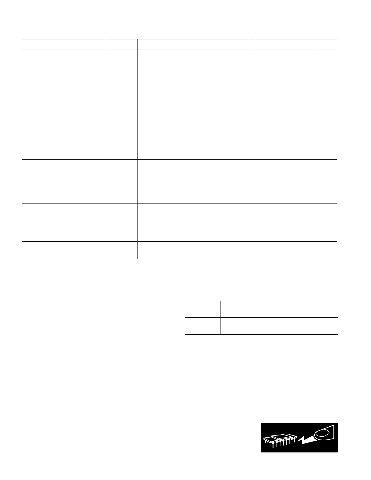
Figure 2. Functional Block Diagram and Typical Speech Application
GENERAL DESCRIPTION
The SSM2166 integrates a complete and flexible solution for
conditioning microphone inputs in computer audio systems. It
is also excellent for improving vocal clarity in communications
and public address systems. A low noise voltage controlled
amplifier (VCA) provides a gain that is dynamically adjusted by
a control loop to maintain a set compression characteristic. The
compression ratio is set by a single resistor and can be varied
from 1:1 to over 15:1 relative to a user defined “rotation
point;” signals above the rotation point are limited to prevent
overload and eliminate “popping.” In the 1:1 compression set-
ting the SSM2166 can be programmed with a fixed gain of up to
One Technology Way, P.O. Box 9106, Norwood, MA 02062-9106, U.S.A.
Tel: 781/329-4700 World Wide Web Site: http://www.analog.com
Fax: 781/326-8703 © Analog Devices, Inc., 1999
CONTROL
AUDIO
+IN
0.1mF
6
BUF
OUT
53
10mF
*
13
V
OUT
9
NOISE GATE
SET
V+
11
ROTATION
POINT SET
10
8
1
GND
22mF
COMPRESSION
RATIO
SET
25kV
2
2.3kV
14
500kV
17kV
1kV
VCA
R
7
LEVEL
DETECTOR
BUFFER
VCA1kV
VCA
IN
SSM2166
4
10mF
R1 = 10kV
R2 = 10kV
1mF
+
12
POWER
DOWN
AVG
CAP
+
++
*OPTIONAL
V+
VCA GAIN
ADJ
Parameter Symbol Conditions Min Typ Max Units
AUDIO SIGNAL PATH
Voltage Noise Density
e
n
15:1 Compression 17 nV/√Hz
Noise 20 kHz Bandwidth, V
IN
= GND –109 dBu
1
Total Harmonic Distortion THD+N 2nd and 3rd Harmonics, V
IN
= –20 dBu 0.25 0.5 %
22 kHz Low-Pass Filter
Input Impedance Z
IN
180 kΩ
Output Impedance Z
OUT
75 Ω
Load Drive Resistive 5 kΩ
Capacitive 2 nF
Buffer
Input Voltage Range 1% THD 1 V rms
Output Voltage Range 1% THD 1 V rms
VCA
Input Voltage Range 1% THD 1 V rms
Output Voltage Range 1% THD 1.4 V rms
Gain Bandwidth Product 1:1 Compression, VCA G = 60 dB 30 MHz
CONTROL SECTION
VCA Dynamic Gain Range 60 dB
VCA Fixed Gain Range –60 to +19 dB
Compression Ratio, Min 1:1
Compression Ratio, Max See Figure 5 for R
COMP
/R
ROT
15:1
Control Feedthrough 15:1 Compression, Rotation Point = –10 dBu ±5mV
POWER SUPPLY
Supply Voltage Range V
S
4.5 5.5 V
Supply Current I
SY
7.5 10 mA
Quiescent Output Voltage Level 2.2 V
Power Supply Rejection Ratio PSRR 50 dB
POWER DOWN
Supply Current Pin 12 = V+
2
10 100 µA
NOTES
1
0 dBu = 0.775 V rms.
2
Normal operation: Pin 12 = 0 V.
Specifications subject to change without notice.
REV. A
– 2 –
CAUTION
ESD (electrostatic discharge) sensitive device. Electrostatic charges as high as 4000 V readily
accumulate on the human body and test equipment and can discharge without detection.
Although the SSM2166 features proprietary ESD protection circuitry, permanent damage may
occur on devices subjected to high energy electrostatic discharges. Therefore, proper ESD
precautions are recommended to avoid performance degradation or loss of functionality.
SSM2166–SPECIFICATIONS
ORDERING GUIDE
Temperature Package Package
Model Range Description Option
SSM2166P –40°C to +85°C Plastic DIP N-14
SSM2166S –40°C to +85°C Narrow SOIC SO-14
ABSOLUTE MAXIMUM RATINGS
Supply Voltage . . . . . . . . . . . . . . . . . . . . . . . . . . . . . . . . .+10 V
Audio Input Voltage . . . . . . . . . . . . . . . . . . . . .Supply Voltage
Operating Temperature Range . . . . . . . . . . . . –40°C to +85°C
Storage Temperature Range . . . . . . . . . . . . . –65°C to +150°C
Junction Temperature (T
J
) . . . . . . . . . . . . . . . . . . . . . +150°C
Lead Temperature (Soldering, 60 sec) . . . . . . . . . . . . +300°C
ESD RATINGS
883 (Human Body) Model . . . . . . . . . . . . . . . . . . . . . . 2.0 kV
THERMAL CHARACTERISTICS
Thermal Resistance
14-Lead Plastic DIP
θ
JA
. . . . . . . . . . . . . . . . . . . . . . . . . . . . . . . . . . . . 83°C/W
θ
JC
. . . . . . . . . . . . . . . . . . . . . . . . . . . . . . . . . . . . 39°C/W
14-Lead SOIC
θ
JA
. . . . . . . . . . . . . . . . . . . . . . . . . . . . . . . . . . . 120°C/W
θ
JC
. . . . . . . . . . . . . . . . . . . . . . . . . . . . . . . . . . . . 36°C/W
(V+ = +5 V, f = 1 kHz, R
L
= 100 kΩ, R
GATE
= 600 kΩ, R
ROTATION
= 3 kΩ, R
COMP
= 0 Ω,
R1 = 0 Ω, R2
= ∞⍀, T
A
= +25ⴗC, unless otherwise noted, V
IN
= 300 mV rms.)
WARNING!
ESD SENSITIVE DEVICE

SSM2166
REV. A
–3–
PIN DESCRIPTION
Pin # Mnemonic Function
1 GND Ground
2 GAIN ADJUST VCA Gain Adjust Pin. A resistor from this pin to ground sets the fixed gain of the VCA. To
check the setting of this pin the compression pin (Pin 10) should be grounded for no com-
pression. The gain can be varied from 0 dB to 20 dB. For 20 dB leave the pin open. For
0 dB of fixed gain, a typical resistor value is approximately 1 kΩ. For 10 dB of fixed gain, the
resistor value is approximately 2 kΩ–3␣ kΩ. For resistor values < 1 kΩ, the VCA can attenu-
ate or mute. Refer to Figure 6.
3 VCA
IN
VCA Input Pin. A typical connection is a 10 µF capacitor from the buffer output pin (Pin 5)
to this pin.
4 VCA
R
Inverting Input to the VCA. This input can be used as a nonground reference for the audio
input signal (see application notes).
5 BUF OUT Input Buffer Amplifier Output Pin. Must not be loaded by capacitance to ground.
6 –IN Inverting Input to the Buffer. A 10 kΩ feedback resistor R1 from the buffer output Pin 5 to
this input pin, and a resistor R2, from this pin through a 1 µF to ground gives gains of 6 dB
to 20 dB for R2 = 10 kΩ to 1.1 kΩ.
7 AUDIO +IN Input Audio Signal. The input signal should be ac-coupled (0.1 µF typical) into this pin.
8 AVG CAP Detector Averaging Capacitor. A capacitor, 2.2 µF–22 µF, to ground from this pin is the
averaging capacitor for the detector circuit.
9 NOISE GATE SET Noise Gate Threshold Set Point. A resistor to V+ sets the level below which input signals are
downward-expanded. For a 0.7 mV threshold, the resistor value is approximately 380 kΩ.
Increasing the resistor value reduces the threshold. See Figure 4.
10 COMP RATIO SET Compression Ratio Set Pin. A resistor to ground from this pin sets the compression ratio as
shown in Figure 1. Figure 5 gives resistor values for various rotation points.
11 ROTATION SET Rotation Point Set Pin. This is set by a resistor to the positive supply. This resistor together
with the gain adjust pin determines the onset of limiting. A typical value for this resistor is
17K for a 100 mV “rotation point.” Increasing the resistor value reduces the level at which
limiting occurs. Refer to Figure 9.
12 POWER DOWN Power-Down Pin. Connect to ground for normal operation. Connect to positive supply for
power-down mode.
13 OUTPUT Output Signal.
14 V+ Positive Supply, +5 V Nominal.
PIN CONFIGURATION
14
13
12
11
10
9
8
1
2
3
4
7
6
5
TOP VIEW
(Not to Scale)
GND
ROTATION SET
POWER DOWN
OUTPUT
V+
GAIN ADJUST
VCA
IN
VCA
R
SSM2166
AVG CAP
NOISE GATE SET
COMP RATIO SET
BUF OUT
–IN
AUDIO +IN

SSM2166
REV. A
–4–
0
–80
–80 0–70 –60 –50 –40 –30 –20 –10
–10
–40
–50
–60
–70
–20
–30
T
A
= +25°C
V+ = 5V
V
IN
= 300mV rms @ 1kHz
R
L
= 100kV
NOISE GATE SETTING
550µV rms
ROTATION POINT 300mV rms
GAIN ADJUST (PIN 2) = 1.25kV
COMP RATIO = 1:1
COMP RATIO = 2:1
COMP RATIO = 5:1
COMP RATIO = 10:1
COMP RATIO = 15:1
INPUT – dBu
OUTPUT – dBu
INPUT – dBu
Figure 3. Output vs. Input Characteristics
R
GATE
– kV
NOISE GATE – mV rms
10
1
0.1
0 45050 100 350 400150 200 250 300 500 550 600 650
100
T
A
= +25°C
V+ = 5V
R
L
= 100kV
COMPRESSION RATIO = 2:1
ROTATION POINT
1V rms
GAIN ADJUST (PIN 2) = 1.25kV
Figure 4. Noise Gate vs. R
GATE
(Pin 9 to V+)
COMPRESSION
RATIO
ROTATION POINT
1:1 2:1 5:1 10:1 15:1
100mV rms 0
300mV rms 0
1V rms 0
12.5
12.5
12.5
96
96
96
215
215
215
395
395
395
R
COMP
– kV, TYPICAL
Figure 5. Compression Ratio vs. R
COMP
(Pin 10 to GND)
GAIN – dB
GAIN ADJUST RESISTOR – kV
20
6
0
0262 4 6 8 10 12 14 16 18 20 22 24
18
8
4
2
14
10
16
12
28 30
T
A
= +25°C
V+ = 5V
R
L
= 100kV
V
IN
= 100mV rms @ 1kHz
NOISE GATE SETTING
550mV rms
ROTATION POINT (PIN 11)
1V rms
COMPRESSION RATIO = 1:1
Figure 6. VCA Gain vs. R
GAIN
(Pin 2 to GND)
INPUT VOLTAGE – V rms
THD + N – %
5
1
0.1
0.01 10.1
0.05
R
L
= 10kV
R
L
= 100kV
T
A
= +25°C
V+ = 5V
COMPRESSION RATIO = 1:1
NOISE GATE SETTING
550mV rms
ROTATION POINT 1V rms
GAIN ADJUST (PIN 2) = 1.25kV
V
IN
FREQUENCY = 1kHz
Figure 7. THD+N (%) vs. Input (V rms)
FREQUENCY – Hz
THD + N – %
5
1
0.1
20 30k100
0.05
1k 10k
T
A
= +25°C
V+ = 5V
V
IN
= 77.5mV rms @ 1kHz
COMPRESSION RATIO = 1:1
NOISE GATE SETTING
550mV rms
ROTATION POINT 1V rms
GAIN ADJUST (PIN 2) = 1.2kV
MEASUREMENT FILTER BW : 22Hz TO 30kHz
Figure 8. THD+N (%) vs. Frequency (Hz)

SSM2166
REV. A
–5–
ROTATION POINT – V rms
R
ROT PT
RESISTOR – kV
1.0
0.1
0.01
045510 354015 20 25 30 50 55
T
A
= +25°C
V+ = 5V
R
L
= 100kV
COMPRESSION RATIO = 1:1
NOISE GATE SETTING
550mV rms
GAIN ADJUST (PIN 2) = 1.25kV
60 65 70 75 80 85 90
Figure 9. Rotation Point vs. R
ROT PT
(Pin 11 to V+)
10
0%
100
90
1s
5
m
V
T
A
= +25 C
COMPRESSION RATIO = 15:1
NOISE BW = 20kHz
Figure 10a. Wideband Output Noise
FREQUENCY – Hz
GAIN – dB
70
60
–20
1k 1M10k 100k
50
40
0
30
20
10
–10
ROTATION POINT = 1.13V rms
NOISE GATE SETTING = 336mV rms
R
COMP
= 40kV
V
IN
= 400mV rms
G = 60dB
G = 40dB
G = 20dB
Figure 10b. GBW Curves vs. VCA Gain
FREQUENCY – Hz
–10
–80
20 30k100 1k
–20
–30
–40
–50
–60
–70
R
COMP
= 0
R
GAIN
= 1.24kV
R
GATE
= 500kV
R
ROT
= 1.74kV
10k
V+ = 5±1V p-p
V+ = 5±0.5V p-p
PSRR – dB
Figure 10c. PSRR vs. Frequency
10
0%
100
90
20mV
10
m
s
T
A
= +25 C
C
AVG
= 2.2mF
SYSTEM GAIN = 0dB
R
L
= 10kV
COMP RATIO = 1:1
Figure 11. Small Signal Transient Response
10
0%
100
90
10
m
s
200mV
T
A
= +25 C
C
AVG
= 2.2mF
SYSTEM GAIN = 0dB
R
L
= 10kV
COMP RATIO = 1:1
Figure 12. Large Signal Transient Response
Loading...