


 Loading...
Analog Devices OP27AZ, OP27FP, OP27GP, OP27EJ, OP27EP Datasheet
...
a |
Low-Noise, Precision |
|
Operational Amplifier |
||
|
|
|
|
|
OP27 |
|
|
|
FEATURES
Low Noise: 80 nV p-p (0.1 Hz to 10 Hz), 3 nV/√Hz Low Drift: 0.2 V/ C
High Speed: 2.8 V/ s Slew Rate, 8 MHz Gain
Bandwidth
Low VOS: 10 V
Excellent CMRR: 126 dB at VCM of ±11 V High Open-Loop Gain: 1.8 Million
Fits 725, OP07, 5534A Sockets Available in Die Form
GENERAL DESCRIPTION
The OP27 precision operational amplifier combines the low offset and drift of the OP07 with both high speed and low noise. Offsets down to 25 µV and drift of 0.6 µV/°C maximum make the OP27 ideal for precision instrumentation applications. Exceptionally low noise, en = 3.5 nV/√Hz, at 10 Hz, a low 1/f noise corner frequency of 2.7 Hz, and high gain (1.8 million), allow accurate high-gain amplification of low-level signals. A gain-bandwidth product of 8 MHz and a 2.8 V/µsec slew rate provides excellent dynamic accuracy in high-speed, dataacquisition systems.
A low input bias current of ± 10 nA is achieved by use of a bias-current-cancellation circuit. Over the military temperature range, this circuit typically holds IB and IOS to ±20 nA and 15 nA, respectively.
The output stage has good load driving capability. A guaranteed swing of ± 10 V into 600 Ω and low output distortion make the OP27 an excellent choice for professional audio applications.
(Continued on page 7)
PIN CONNECTIONS
|
TO-99 |
|
|
(J-Suffix) |
|
|
BAL |
|
BAL 1 |
OP27 |
V+ |
|
|
|
–IN 2 |
|
OUT |
+IN 3 |
|
NC |
|
4V– (CASE) |
|
NC = NO CONNECT
8-Pin Hermetic DIP (Z-Suffix)
Epoxy Mini-DIP (P-Suffix) 8-Pin SO (S-Suffix)
V |
TRIM |
1 |
8 |
V |
TRIM |
OS |
|
|
OP27 |
OS |
|
|
|
|
V+ |
|
|
|
–IN |
2 |
7 |
|
|
|
+IN |
3 |
6 |
OUT |
|
|
V– |
4 |
5 |
NC |
|
|
|
NC = NO CONNECT |
|
|
|
|
|
|
|
|
|
|
|
V+ |
R3 |
1 |
8 |
R4 |
C2 |
|
|
|
|
|
|
|
|
|
||||
Q6 |
|
|
|
|
|
|
||
|
|
|
|
|
Q22 |
|
Q46 |
|
|
VOS ADJ. |
|
|
|
C1 |
|||
R1* |
R2* |
R23 |
R24 |
|
|
|||
|
|
|
||||||
|
|
|
|
Q21 |
|
|
|
|
|
|
|
|
Q23 |
Q24 |
|
R9 |
|
|
|
|
|
|
|
|
|
|
|
|
|
|
|
|
|
Q20 |
Q19 |
Q1A |
Q1B |
Q2B |
Q2A |
|
|
|
R12 |
OUTPUT |
NONINVERTING |
|
|
|
|
R5 |
C3 |
C4 |
|
INPUT (+) |
|
|
|
|
|
|||
|
|
|
|
|
|
|
|
|
Q3 |
|
|
|
|
|
|
|
|
INVERTING |
|
|
Q11 |
Q12 |
|
|
Q26 |
Q45 |
INPUT (–) |
|
|
|
|
|
|||
|
|
|
|
|
|
|
|
|
|
|
|
|
Q27 |
Q28 |
|
|
|
*R1 AND R2 ARE PERMANENTLY |
|
|
|
|
|
|
|
|
ADJUSTED AT WAFER TEST FOR |
|
|
|
|
|
|
|
|
MINIMUM OFFSET VOLTAGE. |
|
|
|
|
|
|
|
|
|
|
|
|
|
|
|
|
V– |
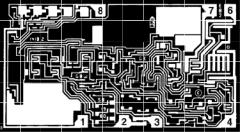
Figure 1. Simplified Schematic
REV. A
Information furnished by Analog Devices is believed to be accurate and reliable. However, no responsibility is assumed by Analog Devices for its use, nor for any infringements of patents or other rights of third parties that may result from its use. No license is granted by implication or otherwise under any patent or patent rights of Analog Devices.
One Technology Way, P.O. Box 9106, Norwood, MA 02062-9106, U.S.A.
Tel: 781/329-4700 |
www.analog.com |
Fax: 781/326-8703 |
© Analog Devices, Inc., 2002 |
OP27–SPECIFICATIONS
ELECTRICAL CHARACTERISTICS (@ VS = ±15 V, TA = 25 C, unless otherwise noted.)
|
|
|
|
OP27A/E |
|
OP27F |
|
OP27C/G |
|
||||
Parameter |
Symbol |
Conditions |
Min |
Typ |
Max |
Min |
Typ |
Max |
Min |
Typ |
Max |
Unit |
|
|
|
|
|
|
|
|
|
|
|
|
|
|
|
INPUT OFFSET |
|
|
|
|
|
|
|
|
|
|
|
|
µV |
VOLTAGE1 |
VOS |
|
|
|
10 |
25 |
|
20 |
60 |
|
30 |
100 |
|
LONG-TERM VOS |
|
|
|
|
|
|
|
|
|
|
|
|
µV/MO |
STABILITY2, 3 |
VOS/Time |
|
|
|
0.2 |
1.0 |
|
0.3 |
1.5 |
|
0.4 |
2.0 |
|
INPUT OFFSET |
|
|
|
|
7 |
35 |
|
9 |
50 |
|
12 |
75 |
nA |
CURRENT |
IOS |
|
|
|
|
|
|||||||
INPUT BIAS |
|
|
|
|
± 10 |
± 40 |
|
± 12 |
± 55 |
|
± 15 |
± 80 |
|
CURRENT |
IB |
|
|
|
|
|
nA |
||||||
INPUT NOISE |
|
|
|
|
|
|
|
|
|
|
|
|
µV p-p |
VOLTAGE3, 4 |
en p-p |
0.1 Hz to 10 Hz |
|
0.08 |
0.18 |
|
0.08 |
0.18 |
|
0.09 |
0.25 |
||
INPUT NOISE |
en |
fO = 10 Hz |
|
3.5 |
5.5 |
|
3.5 |
5.5 |
|
3.8 |
8.0 |
nV/√Hz |
|
Voltage Density3 |
|
fO = 30 Hz |
|
3.1 |
4.5 |
|
3.1 |
4.5 |
|
3.3 |
5.6 |
nV/√Hz |
|
|
|
fO = 1000 Hz |
|
3.0 |
3.8 |
|
3.0 |
3.8 |
|
3.2 |
4.5 |
nV/√Hz |
|
INPUT NOISE |
in |
fO = 10 Hz |
|
1.7 |
4.0 |
|
1.7 |
4.0 |
|
1.7 |
|
pA/√Hz |
|
Current Density3, 5 |
|
fO = 30 Hz |
|
1.0 |
2.3 |
|
1.0 |
2.3 |
|
1.0 |
|
pA/√Hz |
|
|
|
fO = 1000 Hz |
|
0.4 |
0.6 |
|
0.4 |
0.6 |
|
0.4 |
0.6 |
pA/√Hz |
|
INPUT |
|
|
|
|
|
|
|
|
|
|
|
|
|
RESISTANCE |
|
|
|
|
|
|
|
|
|
|
|
|
MΩ |
Differential-Mode6 |
RIN |
|
|
1.3 |
6 |
|
0.94 |
5 |
|
0.7 |
4 |
|
|
Common-Mode |
RINCM |
|
|
|
3 |
|
|
2.5 |
|
|
2 |
|
GΩ |
INPUT VOLTAGE |
|
|
|
± 11.0 |
± 12.3 |
|
± 11.0 |
± 12.3 |
|
± 11.0 |
± 12.3 |
|
|
RANGE |
IVR |
|
|
|
|
|
V |
||||||
COMMON-MODE |
|
VCM = ± 11 V |
|
|
|
|
|
|
|
|
|
|
|
REJECTION RATIO |
CMRR |
114 |
126 |
|
106 |
123 |
|
100 |
120 |
|
dB |
||
|
|
|
|
|
|
|
|
|
|
|
|
|
|
POWER SUPPLY |
PSRR |
VS |
= ± 4 V |
|
|
|
|
|
|
|
|
|
µV/V |
REJECTION RATIO |
|
to ± 18 V |
|
1 |
10 |
|
1 |
10 |
|
2 |
20 |
||
LARGE-SIGNAL |
AVO |
RL ≥ 2 kΩ, |
|
|
|
|
|
|
|
|
|
|
|
VOLTAGE GAIN |
|
VO |
= ± 10 V |
1000 |
1800 |
|
1000 |
1800 |
|
700 |
1500 |
|
V/mV |
|
|
RL |
≥ 600 Ω, |
|
|
|
|
|
|
|
|
|
|
|
|
VO = ± 10 V |
800 |
1500 |
|
800 |
1500 |
|
600 |
1500 |
|
V/mV |
|
OUTPUT |
|
|
≥ 2 kΩ |
± 12.0 |
± 13.8 |
|
± 12.0 |
± 13.8 |
|
± 11.5 |
± 13.5 |
|
|
VOLTAGE SWING |
VO |
RL |
|
|
|
V |
|||||||
|
|
RL |
≥ 600 Ω |
± 10.0 |
± 11.5 |
|
± 10.0 |
± 11.5 |
|
± 10.0 |
± 11.5 |
|
V |
SLEW RATE7 |
SR |
RL ≥ 2 kΩ |
1.7 |
2.8 |
|
1.7 |
2.8 |
|
1.7 |
2.8 |
|
V/µs |
|
|
|
|
|
|
|
|
|
|
|
|
|
|
|
GAIN |
|
|
|
|
|
|
|
|
|
|
|
|
|
BANDWIDTH |
|
|
|
|
|
|
|
|
|
|
|
|
|
PRODUCT7 |
GBW |
|
|
5.0 |
8.0 |
|
5.0 |
8.0 |
|
5.0 |
8.0 |
|
MHz |
OPEN-LOOP |
|
|
|
|
|
|
|
|
|
|
|
|
|
OUTPUT |
|
|
|
|
|
|
|
|
|
|
|
|
Ω |
RESISTANCE |
RO |
VO = 0, IO = 0 |
|
70 |
|
|
70 |
|
|
70 |
|
||
POWER |
|
|
|
|
|
|
|
|
|
|
|
|
|
CONSUMPTION |
Pd |
VO |
|
|
90 |
140 |
|
90 |
140 |
|
100 |
170 |
mW |
OFFSET |
|
|
|
|
|
|
|
|
|
|
|
|
|
ADJUSTMENT |
|
RP = 10 kΩ |
|
± 4.0 |
|
|
± 4.0 |
|
|
± 4.0 |
|
|
|
RANGE |
|
|
|
|
|
|
|
mV |
|||||
|
|
|
|
|
|
|
|
|
|
|
|
|
|
NOTES
1Input offset voltage measurements are performed ~ 0.5 seconds after application of power. A/E grades guaranteed fully warmed up.
2Long-term input offset voltage stability refers to the average trend line of VOS versus. Time over extended periods after the first 30 days of operation. Excluding the initial hour of operation, changes in VOS during the first 30 days are typically 2.5 V. Refer to typical performance curve.
3Sample tested.
4See test circuit and frequency response curve for 0.1 Hz to 10 Hz tester. 5See test circuit for current noise measurement.
6Guaranteed by input bias current.
7Guaranteed by design.
–2– |
REV. A |
|
|
|
|
|
|
|
|
|
OP27 |
|
ELECTRICAL CHARACTERISTICS (@ VS = ±15 V, –55 C ≤ TA ≤ 125 C, unless otherwise noted.) |
|
|
|
|||||||
|
|
|
|
|
|
|
|
|
|
|
|
|
|
|
OP27A |
|
|
OP27C |
|
|
|
Parameter |
Symbol |
Conditions |
Min |
Typ |
Max |
Min |
Typ |
Max |
Unit |
|
|
|
|
|
|
|
|
|
|
|
|
INPUT OFFSET |
|
|
|
|
|
|
|
|
µV |
|
VOLTAGE1 |
VOS |
|
|
30 |
60 |
|
70 |
300 |
||
AVERAGE INPUT |
TCVOS2 |
|
|
|
|
|
|
|
|
|
OFFSET DRIFT |
|
|
|
|
|
|
|
µV/°C |
||
|
3 |
|
|
0.2 |
0.6 |
|
4 |
1.8 |
||
|
TCVOSn |
|
|
|
||||||
INPUT OFFSET |
|
|
|
|
|
|
|
|
|
|
CURRENT |
IOS |
|
|
15 |
50 |
|
30 |
135 |
nA |
|
INPUT BIAS |
|
|
|
± 20 |
± 60 |
|
± 35 |
± 150 |
|
|
CURRENT |
IB |
|
|
|
nA |
|||||
INPUT VOLTAGE |
|
|
± 10.3 |
± 11.5 |
|
± 10.2 |
± 11.5 |
|
|
|
RANGE |
IVR |
|
|
|
V |
|||||
|
|
|
|
|
|
|
|
|
|
|
COMMON-MODE |
|
VCM = ± 10 V |
|
|
|
|
|
|
|
|
REJECTION RATIO |
CMRR |
108 |
122 |
|
94 |
118 |
|
dB |
||
|
|
|
|
|
|
|
|
|
|
|
POWER SUPPLY |
|
VS = ± 4.5 V to ± 18 V |
|
|
|
|
|
|
µV/V |
|
REJECTION RATIO |
PSRR |
|
2 |
16 |
|
4 |
51 |
|||
|
|
|
|
|
|
|
|
|
|
|
LARGE-SIGNAL |
|
RL ≥ 2 kΩ, VO = ± 10 V |
|
|
|
|
|
|
|
|
VOLTAGE GAIN |
AVO |
600 |
1200 |
|
300 |
800 |
|
V/mV |
||
OUTPUT |
|
RL ≥ 2 kΩ |
± 11.5 |
± 13.5 |
|
± 10.5 |
± 13.0 |
|
|
|
VOLTAGE SWING |
VO |
|
|
V |
|
|||||
NOTES
1Input offset voltage measurements are performed by automated test equipment approximately 0.5 seconds after application of power. A/E grades guaranteed fully warmed up.
2The TCVOS performance is within the specifications unnulled or when nulled with RP = 8 kΩ to 20 kΩ. TCVOS is 100% tested for A/E grades, sample tested for C/F/G grades.
3Guaranteed by design.
REV. A |
–3– |
OP27
ELECTRICAL CHARACTERISTICS
(@ VS = ±15 V, –25 C¯≤ TA ≤ 85 C for OP27J, OP27Z, 0 C ≤ TA ≤ 70 C for OP27EP, OP27FP, and –40 C ≤ TA ≤ 85 C for OP27GP, OP27GS, unless otherwise noted.)
|
|
|
OP27E |
|
|
OP27F |
|
OP27G |
|
|
||
Parameter |
Symbol |
Conditions |
Min |
Typ |
Max |
Min |
Typ |
Max |
Min |
Typ |
Max |
Unit |
|
|
|
|
|
|
|
|
|
|
|
|
|
INPUT ONSET |
|
|
|
|
|
|
|
|
|
|
|
µV |
VOLTAGE |
VOS |
|
|
20 |
50 |
|
40 |
140 |
|
55 |
220 |
|
AVERAGE INPUT |
TCVOS1 |
|
|
|
|
|
|
|
|
|
|
µV/°C |
OFFSET DRIFT |
|
|
0.2 |
0.6 |
|
0.3 |
1.3 |
|
0 4 |
1.8 |
||
|
2 |
|
|
0.2 |
0.6 |
|
0.3 |
1.3 |
|
0 4 |
1.8 |
µV/°C |
|
TCVOSn |
|
|
|
|
|||||||
INPUT OFFSET |
|
|
|
|
|
|
|
|
|
|
|
|
CURRENT |
IOS |
|
|
10 |
50 |
|
14 |
85 |
|
20 |
135 |
nA |
INPUT BIAS |
|
|
|
± 14 |
± 60 |
|
± 18 |
± 95 |
|
± 25 |
± 150 |
|
CURRENT |
IB |
|
|
|
|
nA |
||||||
INPUT VOLTAGE |
|
|
± 10.5 |
± 11.8 |
|
± 10.5 |
± 11.8 |
|
± 10.5 |
± 11.8 |
|
|
RANGE |
IVR |
|
|
|
|
V |
||||||
|
|
|
|
|
|
|
|
|
|
|
|
|
COMMON-MODE |
|
VCM = ± 10 V |
|
|
|
|
|
|
|
|
|
|
REJECTION RATIO |
CMRR |
110 |
124 |
|
102 |
121 |
|
96 |
118 |
|
dB |
|
|
|
|
|
|
|
|
|
|
|
|
|
|
POWER SUPPLY |
|
VS = ± 4.5 V |
|
|
|
|
|
|
|
|
|
µV/V |
REJECTION RATIO |
PSRR |
|
2 |
15 |
|
2 |
16 |
|
2 |
32 |
||
|
|
to ± 18 V |
|
|
|
|
|
|
|
|
|
|
|
|
|
|
|
|
|
|
|
|
|
|
|
LARGE-SIGNAL |
|
RL ≥ 2 kΩ, |
|
|
|
|
|
|
|
|
|
|
VOLTAGE GAIN |
AVO |
|
|
|
|
|
|
|
|
|
|
|
|
|
VO = ± 10 V |
750 |
1500 |
|
700 |
1300 |
|
450 |
1000 |
|
V/mV |
OUTPUT |
|
RL ≥ 2 kΩ |
± 11.7 |
± 13.6 |
|
± 11.4 |
± 13.5 |
|
± 11.0 |
± 13.3 |
|
|
VOLTAGE SWING |
VO |
|
|
|
V |
|||||||
NOTES
1The TCVOS performance is within the specifications unnulled or when nulled with RP = 8 kΩ to 20 kΩ. TCVOS is 100% tested for A/E grades, sample tested for C/F/G grades.
2Guaranteed by design.
–4– |
REV. A |
OP27
DICE CHARACTERISTICS
|
|
|
1. NULL |
|
|
|
|
|
|
|
2. (–) INPUT |
|
|
||
|
|
|
3. (+) INPUT |
|
|
||
|
|
|
4. V– |
|
|
|
|
|
|
|
6. OUTPUT |
|
|
||
|
|
|
7. V+ |
|
|
|
|
|
|
|
8. NULL |
|
|
|
|
|
DIE SIZE 0.109 0.055 INCH, 5995 SQ. MILS |
|
|
|
|
|
|
|
|
(2.77 1.40mm, 3.88 SQ. mm) |
|
|
|
|
|
WAFER TEST LIMITS (@ VS = ±15 V, TA = 25 C unless otherwise noted.) |
|
|
|
|
|
||
|
|
|
|
|
|
|
|
|
|
|
OP27N |
|
OP27G |
OP27GR |
|
Parameter |
Symbol |
Conditions |
Limit |
|
Limit |
Limit |
Unit |
|
|
|
|
|
|
|
|
INPUT OFFSET VOLTAGE* |
VOS |
|
35 |
|
60 |
100 |
µV Max |
INPUT OFFSET CURRENT |
IOS |
|
35 |
|
50 |
75 |
nA Max |
INPUT BIAS CURRENT |
IB |
|
± 40 |
|
± 55 |
± 80 |
nA Max |
INPUT VOLTAGE RANGE |
IVR |
|
± 11 |
|
± 11 |
± 11 |
V Min |
COMMON-MODE REJECTION |
|
|
|
|
|
|
|
RATIO |
CMRR |
VCM = IVR |
114 |
|
106 |
100 |
dB Min |
POWER SUPPLY |
PSRR |
VS = ± 4 V to ± 18 V |
10 |
|
10 |
20 |
µV/V Max |
LARGE-SIGNAL VOLTAGE |
|
RL ≥ 2 kΩ, VO = ± 10 V |
|
|
|
|
|
GAIN |
AVO |
1000 |
|
1000 |
700 |
V/mV Min |
|
|
AVO |
RL ≥ 600 Ω, VO = ± 10 V |
800 |
|
800 |
600 |
V/mV Min |
OUTPUT VOLTAGE SWING |
VO |
RL ≥ 2 kΩ |
± 12.0 |
|
± 12.0 |
+11.5 |
V Min |
|
VO |
RL2600n |
± 10.0 |
|
± 10.0 |
± 10.0 |
V Min |
POWER CONSUMPTION |
Pd |
VO = 0 |
140 |
|
140 |
170 |
mW Max |
NOTE
*Electrical tests are performed at wafer probe to the limits shown. Due to variations in assembly methods and normal yield loss, yield after packaging is not guaranteed for standard product dice. Consult factory to negotiate specifications based on dice lot qualification through sample lot assembly and testing.
REV. A |
–5– |
Loading...