


a QuadLowOperationalVoltage MicropowerAmplifier
OP490
FEATURES
Single/Dual-Supply Operation
1.6 V to 36 V
0.8 V to 18 V
True Single-Supply Operation; Input and Output
Voltage Ranges Include Ground
Low Supply Current: 80 A Max
High Output Drive: 5 mA Min
Low Offset Voltage: 0.5 mA Max
High Open-Loop Gain: 700 V/mV Min
Outstanding PSRR: 5.6 mV/V Min
Industry Standard Quad Pinouts
Available in Die Form
GENERAL DESCRIPTION
The OP490 is a high-performance micropower quad op amp that operates from a single supply of 1.6 V to 36 V or from dual supplies of ±0.8 V to ±18 V. Input voltage range includes the negative rail allowing the OP490 to accommodate input signals down to ground in single-supply operation. The OP490’s output swing also includes ground when operating from a single supply, enabling “zero-in, zero-out” operation.
The quad OP490 draws less than 20 μA of quiescent supply current per amplifier, but each amplifier is able to deliver over 5 mA of output current to a load. Input offset voltage is under 0.5 mV with offset drift below 5 μV/∞C over the military temperature range. Gain exceeds over 700,000 and CMR is better than 100 dB. A PSRR of under 5.6 μV/V minimizes offset voltage changes experienced in battery-powered systems.
The quad OP490 combines high performance with the space and cost savings of quad amplifiers. The minimal voltage and current requirements of the OP490 make it ideal for batteryand solar-powered applications, such as portable instruments and remote sensors.
PIN CONNECTION
14-Lead Hermetic DIP
(Y Suffix)
OUT A |
1 |
14 |
OUT D |
ñIN A |
2 |
13 |
ñIN D |
+IN A |
3 |
12 |
+IN D |
V+ |
4 |
11 |
Vñ |
+IN B |
5 |
10 |
+IN C |
ñIN B |
6 |
9 |
ñIN C |
OUT B |
7 |
8 |
OUT C |
14-Lead Plastic DIP
(P Suffix)
OUT A |
1 |
14 |
OUT D |
ñIN A |
2 |
13 |
ñIN D |
+IN A |
3 |
12 |
+IN D |
V+ |
4 |
11 |
Vñ |
+IN B |
5 |
10 |
+IN C |
ñIN B |
6 |
9 |
ñIN C |
OUT B |
7 |
8 |
OUT C |
|
16-Lead SOIC |
|
|
|
|
(S Suffix) |
|
OUT A |
1 |
16 |
OUT D |
ñIN A |
2 |
15 |
ñIN D |
+IN A |
3 |
14 |
+IN D |
V+ |
4 |
13 |
Vñ |
+IN B |
5 |
12 |
+IN C |
ñIN B |
6 |
11 |
ñIN C |
OUT B |
7 |
10 |
OUT C |
NC |
8 |
9 |
NC |
|
NC = NO CONNECT |
|
|
REV. C
Information furnished by Analog Devices is believed to be accurate and reliable. However, no responsibility is assumed by Analog Devices for its use, nor for any infringements of patents or other rights of third parties that may result from its use. No license is granted by implication or otherwise under any patent or patent rights of Analog Devices.
One Technology Way, P.O. Box 9106, Norwood, MA 02062-9106, U.S.A.
Tel: 781/329-4700 |
www.analog.com |
Fax: 781/326-8703 |
© Analog Devices, Inc., 2002 |
OP490–SPECIFICATIONS
ELECTRICAL CHARACTERISTICS (@ VS = 1.5 V to 15 V, TA = 25 C, unless otherwise noted)
|
|
|
|
OP490E |
|
|
OP490F |
|
|
OP490G |
|
|
Parameter |
Symbol |
Conditions |
Min |
Typ |
Max |
Min |
Typ |
Max |
Min |
Typ |
Max |
Unit |
|
|
|
|
|
|
|
|
|
|
|
|
|
Input Offset |
|
|
|
|
|
|
|
|
|
|
|
|
Voltage |
VOS |
|
|
0.2 |
0.5 |
|
0.4 |
0.75 |
|
0.6 |
1.0 |
mV |
Input Offset |
|
|
|
|
|
|
|
|
|
|
|
|
Current |
IOS |
VCM = 0 V |
|
0.4 |
3.0 |
|
0.4 |
5 |
|
0.4 |
5 |
nA |
Input Bias |
|
|
|
|
|
|
|
|
|
|
|
|
Current |
IB |
VCM = 0 V |
|
4.2 |
15.0 |
|
4.2 |
20 |
|
4.2 |
25 |
nA |
Large Signal |
AVO |
VS = ± 15 V, VO = ± 10 V, |
|
|
|
|
|
|
|
|
|
|
Voltage Gain |
|
RL = 100 kΩ |
700 |
1,200 |
|
500 |
1,000 |
|
400 |
800 |
|
V/mV |
|
|
RL = 10 kΩ |
350 |
600 |
|
250 |
500 |
|
200 |
400 |
|
V/mV |
|
|
RL = 2 kΩ |
125 |
250 |
|
100 |
200 |
|
100 |
200 |
|
V/mV |
|
|
V+ = 5 V, V– = 0 V, |
|
|
|
|
|
|
|
|
|
|
|
|
1 V < VO < 4 V |
|
|
|
|
|
|
|
|
|
|
|
|
RL = 100 kΩ |
200 |
400 |
|
125 |
300 |
|
100 |
250 |
|
V/mV |
|
|
RL = 10 kΩ |
100 |
180 |
|
75 |
140 |
|
70 |
140 |
|
V/mV |
Input Voltage |
IVR |
V+ = 5 V, V– = 0 V |
0/4 |
|
|
0/4 |
|
|
0/4 |
|
|
V |
Range |
|
VS = ± 15 V1 |
–15/+13.5 |
|
–15/+13.5 |
|
–15/+13.5 |
|
V |
|||
Output Voltage |
VO |
VS = ± 15 V, RL = 10 kΩ |
± 13.5 |
± 14.2 |
|
± 13.5 |
± 14.2 |
|
± 13.5 |
± 14.2 |
|
V |
Swing |
|
RL = 2 kΩ |
± 10.5 |
± 11.5 |
|
± 10.5 |
± 11.5 |
|
± 10.5 |
± 11.5 |
|
V |
|
VOH |
V+ = 5 V, V– = 0 V, |
|
|
|
|
|
|
|
|
|
|
|
|
RL = 2 kΩ |
4.0 |
4.2 |
|
4.0 |
4.2 |
|
4.0 |
4.2 |
|
V |
|
VOL |
V+ = 5 V, V– = 0 V, |
|
|
|
|
|
|
|
|
|
|
|
|
RL = 10 kΩ |
|
100 |
500 |
|
100 |
500 |
|
100 |
500 |
μV |
Common-Mode |
CMRR |
V+ = 5 V, V– = 0 V, |
90 |
110 |
|
80 |
100 |
|
800 |
100 |
|
dB |
Rejection Ratio |
|
0 V < VCM < 4 V |
|
|
|
|
|
|
|
|
|
|
|
|
VS = ± 15 V, |
100 |
130 |
|
90 |
120 |
|
90 |
120 |
|
dB |
|
|
–15 V < VCM < +13.5 V |
|
|
|
|
|
|
|
|
|
|
Power Supply |
|
|
|
|
|
|
|
|
|
|
|
μV/V |
Rejection Ratio |
PSRR |
|
|
1.0 |
5.6 |
|
3.2 |
10 |
|
3.2 |
10 |
|
|
|
|
|
|
|
|
|
|
|
|
|
|
Slew Rate |
SR |
VS = ± 15 V |
5 |
12 |
|
5 |
12 |
|
5 |
12 |
|
V/ms |
|
|
|
|
|
|
|
|
|
|
|
|
|
Supply Current |
|
VS = ±1.5 V, No Load |
|
40 |
60 |
|
40 |
60 |
|
40 |
60 |
μA |
(All Amplifiers) |
ISY |
VS = ±15 V, No Load |
|
60 |
80 |
|
60 |
80 |
|
60 |
80 |
μA |
Capacitive Load |
|
AV = 1 |
|
650 |
|
|
650 |
|
|
650 |
|
pF |
Stability |
|
|
|
|
|
|
|
|
|
|
|
|
|
|
|
|
|
|
|
|
|
|
|
|
|
Input Noise |
en p-p |
fO = 0.1 Hz to 10 Hz, |
|
|
|
|
|
|
|
|
|
|
Voltage |
|
VS = ± 15 V |
|
3 |
|
|
3 |
|
|
3 |
|
μV p-p |
Input Resistance |
|
VS = ± 15 V |
|
|
|
|
|
|
|
|
|
MΩ |
Differential Mode |
RIN |
|
30 |
|
|
30 |
|
|
30 |
|
||
Input Resistance |
|
VS = ± 15 V |
|
|
|
|
|
|
|
|
|
GΩ |
Common-Mode |
RINCM |
|
20 |
|
|
20 |
|
|
20 |
|
||
Gain Bandwidth |
|
|
|
|
|
|
|
|
|
|
|
|
Product |
GBWP |
AV = 1 |
|
20 |
|
|
20 |
|
|
20 |
|
kHz |
Channel Separation |
CS |
fO = 10 Hz, VO = 20 V p-p |
120 |
150 |
|
120 |
150 |
|
120 |
150 |
|
dB |
|
|
VS = ± 15 V2 |
|
|
|
|
|
|
|
|
|
|
NOTES |
|
|
|
|
|
|
|
|
|
|
|
|
1Guaranteed by CMRR test. |
|
|
|
|
|
|
|
|
|
|
|
|
2Guaranteed but not 100% tested. |
|
|
|
|
|
|
|
|
|
|
|
|
Specifications subject to change without notice |
|
|
|
|
|
|
|
|
|
|
||
–2– |
REV. C |
OP490
|
|
(@ VS = 1.5 V to 15 V, –25 C ≤ TA ≤ +85 C for OP490E/F, –40 C ≤ TA ≤ +125 C for |
||||||||||
ELECTRICAL CHARACTERISTICS OP490G, unless otherwise noted) |
|
|
|
|
|
|
|
|||||
|
|
|
|
OP490E |
|
|
OP490F |
|
|
OP490G |
|
|
Parameter |
Symbol |
Conditions |
Min |
Typ |
Max |
Min |
Typ |
Max |
Min |
Typ |
Max |
Unit |
|
|
|
|
|
|
|
|
|
|
|
|
|
Input Offset |
|
|
|
|
|
|
|
|
|
|
|
|
Voltage |
VOS |
|
|
0.32 |
0.8 |
|
0.6 |
1.35 |
|
0.8 |
1.5 |
mV |
Average Input |
|
VS = ± 15 V |
|
|
|
|
|
|
|
|
|
μV/∞C |
Offset Voltage Drift |
TCVOS |
|
2 |
5 |
|
4 |
|
|
4 |
|
||
Input Offset |
|
|
|
|
|
|
|
|
|
|
|
|
Current |
IOS |
VCM = 0 V |
|
0.8 |
3 |
|
1.0 |
5 |
|
1.3 |
7 |
nA |
Input Bias |
|
|
|
|
|
|
|
|
|
|
|
|
Current |
IB |
VCM = 0 V |
|
4.4 |
15 |
|
4.4 |
20 |
|
4.4 |
25 |
nA |
Large Signal |
AVO |
VS = ± 15 V, VO = ± 10 V, |
|
|
|
|
|
|
|
|
|
|
Voltage Gain |
|
RL = 100 kΩ |
500 |
800 |
|
350 |
700 |
|
300 |
600 |
|
V/mV |
|
|
RL = 10 kΩ |
250 |
400 |
|
175 |
250 |
|
150 |
250 |
|
V/mV |
|
|
RL = 2 kΩ |
100 |
200 |
|
75 |
150 |
|
75 |
125 |
|
V/mV |
|
|
V+ = 5 V, V– = 0 V, |
|
|
|
|
|
|
|
|
|
|
|
|
1 V < VO < 4 V |
|
|
|
|
|
|
|
|
|
|
|
|
RL = 100 kΩ |
150 |
280 |
|
100 |
220 |
|
80 |
160 |
|
V/mV |
|
|
RL = 10 kΩ |
75 |
140 |
|
50 |
110 |
|
40 |
90 |
|
V/mV |
|
|
|
|
|
|
|
|
|
|
|
|
|
Input Voltage |
IVR |
V+ = 5 V, V– = 0 V |
0.3/5 |
|
|
0.3/5 |
|
|
0.3/5 |
|
|
V |
Range |
|
VS = ± 15 V* |
–15/+13.5 |
|
–15/+13.5 |
|
–15/+13.5 |
|
V |
|||
|
|
|
|
|
|
|
|
|
|
|
|
|
Output Voltage |
VO |
VS = ± 15 V, RL = 10 kΩ |
± 13 |
± 14 |
|
± 13 |
± 14 |
|
± 13 |
± 14 |
|
V |
Swing |
|
RL = 2 kΩ |
± 10 |
± 11 |
|
± 10 |
± 11 |
|
± 10 |
± 11 |
|
V |
|
VOH |
V+ = 5 V, V– = 0 V, |
|
|
|
|
|
|
|
|
|
|
|
|
RL = 2 kΩ |
3.9 |
4.1 |
|
3.9 |
4.1 |
|
3.9 |
4.1 |
|
V |
|
VOL |
V+ = 5 V, V– = 0 V, |
|
|
|
|
|
|
|
|
|
|
|
|
RL = 10 kΩ |
|
100 |
500 |
|
100 |
500 |
|
100 |
500 |
μV |
Common-Mode |
CMRR |
V+ = 5 V, V– = 0 V, |
90 |
110 |
|
80 |
100 |
|
800 |
100 |
|
dB |
Rejection Ratio |
|
0 V < VCM < 3.5 V |
|
|
|
|
|
|
|
|
|
|
|
|
VS = ± 15 V, |
100 |
120 |
|
90 |
110 |
|
90 |
110 |
|
dB |
|
|
–15 V < VCM < +13.5 V |
|
|
|
|
|
|
|
|
|
|
Power Supply |
|
|
|
|
|
|
|
|
|
|
|
μV/V |
Rejection Ratio |
PSRR |
|
|
1.0 |
5.6 |
|
3.2 |
10 |
|
5.6 |
17.8 |
|
|
|
|
|
|
|
|
|
|
|
|
|
|
Supply Current |
|
VS = ±1.5 V, No Load |
|
65 |
100 |
|
65 |
100 |
|
60 |
100 |
μA |
(All Amplifiers) |
ISY |
VS = ±15 V, No Load |
|
80 |
120 |
|
80 |
120 |
|
75 |
120 |
μA |
NOTE
*Guaranteed by CMRR test.
Specifications subject to change without notice
REV. C |
–3– |
OP490
WAFER TEST LIMITS (@ VS = 1.5 V to 15 V, TA = 25 C, unless otherwise noted)
Parameter |
Symbol |
Conditions |
Limits |
Unit |
|
|
|
|
|
Input Offset Voltage |
VOS |
|
0.75 |
mV max |
Input Offset Current |
IOS |
VCM = 0 V |
5 |
nA max |
Input Bias Current |
IB |
VCM = 0 V |
20 |
nA max |
Large Signal Voltage Gain |
AVO |
VS = ±15 V, VO = ±10 V, |
|
|
|
|
RL = 100 kΩ |
500 |
V/mV min |
|
|
RL = 10 kΩ |
250 |
V/mV min |
|
|
V+ = 5 V, V– = 0 V |
125 |
V/mV min |
|
|
1 V < VO < 4 V, RL = 100 kΩ |
|
|
Input Voltage Range |
IVR |
V+ = 5 V, V– = 0 V |
0/4 |
V min |
|
|
VS = ±15 V* |
–15/+13.5 |
V min |
Output Voltage Swing |
VO |
VS = ±15 V |
± 13.5 |
|
|
|
RL = 10 kΩ |
V min |
|
|
|
RL = 2 kΩ |
± 10.5 |
V min |
|
VOH |
V+ = 5 V, V– = 0 V, RL = 2 kΩ |
4.0 |
V min |
|
VOL |
V+ = 5 V, V– = 0 V, RL = 10 kΩ |
500 |
μV max |
Common-Mode Rejection Ratio |
CMRR |
V+ = 5 V, V– = 0 V, 0 V < VCM < 4 V |
80 |
dB min |
|
|
VS = ±15 V, –15 V < VCM < +13.5 V |
90 |
dB min |
Power Supply Rejection Ratio |
PSRR |
|
10 |
μV/V max |
|
|
|
|
|
Supply Current (All Amplifiers) |
ISY |
VS = ±15 V, No Load |
80 |
μA max |
NOTE
*Guaranteed by CMRR test.
Electrical tests are performed at wafer probe to the limits shown. Due to variations in assembly methods and normal yield loss, yield after packaging is not guaranteed for standard product dice. Consult factory to negotiate specifications based on dice lot qualifications through sample lot assembly and testing.
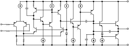
V+ |
+IN |
OUTPUT |
ñIN |
Vñ |
Figure 1. Simplified Schematic
–4– |
REV. C |
OP490
ABSOLUTE MAXIMUM RATINGS* |
±18 V |
|
Supply Voltage . . . . . . . . . . . . . |
. . . . . . . . . . |
|
Digital Input Voltage . . . . . . . . |
[(V–) – 20 V] to [(V+) + 20 V] |
|
Common-Mode Input Voltage |
[(V–) – 20 V] to [(V+) + 20 V] |
|
Output Short Circuit Duration |
. . . . . . . . . . |
. . . . . Continuous |
Storage Temperature Range |
|
–65∞C to +150∞C |
Y and P Packages . . . . . . . . . |
. . . . . . . . . . |
|
Operating Temperature Range |
|
–25∞C to +85∞C |
OP490E, OP490F . . . . . . . . |
. . . . . . . . . . . |
|
OP490G . . . . . . . . . . . . . . . . |
. . . . . . . . . . . |
–40∞C to +85∞C |
Junction Temperature (TJ) . . . |
. . . . . . . . . . |
–65∞C to +150∞C |
Lead Temperature Range (Soldering, 60 sec) |
. . . . . . . . 300∞C |
|
*Stresses above those listed under Absolute Maximum Ratings may cause permanent damage to the device. This is a stress rating only; functional operation of the device at these or any other conditions above those listed in the operational sections of this specification is not implied. Exposure to absolute maximum rating conditions for extended periods may affect device reliability.
Package Type |
JA* |
JC |
Unit |
14-Pin Hermetic DIP (Y) |
99 |
12 |
∞C/W |
14-Pin Plastic DIP (P) |
76 |
33 |
∞C/W |
16-Pin SOL (S) |
92 |
27 |
∞C/W |
*θJA is specified for worst case mounting conditions, i.e., θJA is specified for device in socket for CERDIP and PDIP packages; θJA is specified for device soldered to printed circuit board for SOL package
ORDERING GUIDE
|
Temperature |
Package |
Package |
Model |
Range |
Description |
Option |
|
|
|
|
OP490EY* |
–25∞C to +85∞C |
14-Lead CERDIP |
Y-14 |
OP490FY* |
–25∞C to +85∞C |
14-Lead CERDIP |
Y-14 |
OP490GP |
–40∞C to +85∞C |
14-Lead Plastic DIP |
P-14 |
OP490GS |
–40∞C to +85∞C |
16-Lead SOIC |
S-14 |
*Not recommended for new designs. Obsolete April 2002.
For Military processed devices, please refer to the Standard Microcircuit Drawing (SMD) available at www.dscc.dla.mil/programs/milspec/default.asp
SMD Part Number |
ADI Equivalent |
|
|
5962-89670013A* |
OP490ATCMDA |
5962-8967001CA* |
OP490AYMDA |
|
|
*Not recommended for new designs. Obsolete April 2002.
CAUTION
ESD (electrostatic discharge) sensitive device. Electrostatic charges as high as 4000 V readily accumulate on the human body and test equipment and can discharge without detection. Although the OP490 features proprietary ESD protection circuitry, permanent damage may occur on devices subjected to high-energy electrostatic discharges. Therefore, proper ESD precautions are recommended to avoid performance degradation or loss of functionality.
WARNING!
ESD SENSITIVE DEVICE
REV. C |
–5– |
 Loading...