


SGS Thomson Microelectronics ST485ADR, ST485CN, ST485CDR, ST485CD, ST485BN Datasheet
...ST485
LOW POWER RS-485/RS-422 TRANSCEIVER
■LOW QUIESCENT CURRENT: 300μA
■DESIGNED FOR RS-485 INTERFACE APPLICATIONS
■-7V TO 12V COMMON MODE INPUT VOLTAGE RANGE
■DRIVER MAINTAINS HIGH IMPEDANCE IN 3-STATE OR WITH THE POWER OFF
■70mV TYPICAL INPUT HYSTERESIS
■30ns PROPAGATION DELAYS, 5ns SKEW
■OPERATE FROM A SINGLE 5V SUPPLY
■CURRENT LIMITING AND THERMAL SHUTDOWN FOR DRIVER OVERLOAD PROTECTION
■ALLOWS UP TO 64 TRANSCEIVERS ON THE BUS
DESCRIPTION
The ST485 is al low power transceiver for RS-485 and RS-422 communication. Each part contains one driver and one receiver.
This transceiver draw 300μA (typ.) of supply current when unloaded or fully loaded with disabled drivers.
DIP SOP
It operates from a single 5V supply.
Driver is short-circuit current limited and is protected against excessive power dissipation by thermal shutdown circuitry that placed the driver outputs into a high-impedance state. .
The ST485 is designed for bi-directional data communications on multipoint bus transmission line (half-duplex applciations).
ORDERING CODES
Type |
Temperature |
Package |
Comments |
|
Range |
||||
|
|
|
||
ST485CN |
0 to 70 °C |
DIP-8 |
50parts per tube / 40tube per box |
|
ST485BN |
-40 to 85 °C |
DIP-8 |
50parts per tube / 40tube per box |
|
ST485AN |
-55 to 125 °C |
DIP-8 |
50parts per tube / 40tube per box |
|
ST485CD |
0 to 70 °C |
SO-8 (Tube) |
100parts per tube / 20tube per box |
|
ST485BN |
-40 to 85 °C |
DIP-8 |
50parts per tube / 40tube per box |
|
ST485AD |
-55 to 125 °C |
SO-8 (Tube) |
100parts per tube / 20tube per box |
|
ST485CDR |
0 to 70 °C |
SO-8 (Tape & Reel) |
2500 parts per reel |
|
ST485BDR |
-40 to 85 °C |
SO-8 (Tape & Reel) |
2500 parts per reel |
|
ST485ADR |
-55 to 125 °C |
SO-8 (Tape & Reel) |
2500 parts per reel |
March 2002 |
1/12 |

ST485
PIN CONFIGURATION
PIN DESCRIPTION
PlN N° |
SYMBOL |
NAME AND FUNCTION |
1 |
RO |
Receiver Output |
2 |
RE |
Receiver Output Enable |
3 |
DE |
Driver Output Enable |
4 |
DI |
Driver Input |
5 |
GND |
Ground |
6 |
A |
Non-inverting Receiver Input and Non-inverting Driver Output |
7 |
B |
Inverting Receiver Input and Inverting Driver Output |
8 |
VCC |
Supply Voltage |
TRUTH TABLE (DRIVER) |
|
|
TRUTH TABLE (RECEIVER) |
|
||||
|
INPUTS |
|
OUTPUTS |
|
INPUTS |
|
OUTPUT |
|
RE |
DE |
DI |
B |
A |
RE |
DE |
A-B |
RO |
X |
H |
H |
L |
H |
L |
L |
≥ +0.2V |
H |
X |
H |
L |
H |
L |
L |
L |
≤ -0.2V |
L |
X |
L |
X |
Z |
Z |
L |
L |
INPUTS OPEN |
H |
X= Don't Care; Z=High Impedance |
|
|
H |
L |
X |
Z |
||
|
|
|
|
|
X= Don't Care; Z=High Impedance |
|
||
ABSOLUTE MAXIMUM RATINGS
Symbol |
Parameter |
Value |
VCC |
Supply Voltage |
12 |
VI |
Control Input Voltage (RE, DE) |
-0.5 to (VCC + 0.5) |
VDI |
Driver Input Voltage (DI) |
-0.5 to (VCC + 0.5) |
VDO |
Driver Output Voltage (A, B) |
± 14 |
VRI |
Receiver Input Voltage (A, B) |
± 14 |
VRO |
Receiver Output Voltage (RO) |
-0.5 to (VCC + 0.5) |
Unit
V
V
V
V
V
V
Absolute Maximum Ratings are those values beyond which damage to the device may occur. Functional operation under these condition is not implied.
2/12

ST485
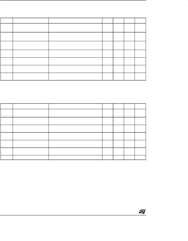
DC ELECTRICAL CHARACTERISTICS
(VCC = 5V ± 5%, TA = TMIN to TMAX , unless otherwise specified. Typical values are referred to TA = 25°C) (See Note 1)
Symbol |
Parameter |
Test Conditions |
Min. |
Typ. Max. |
Unit |
VOD1 |
Differential Driver Output |
|
|
5 |
V |
|
(No Load) |
|
|
|
|
VOD2 |
Differential Driver Output |
|
(With Load) |
VOD |
Change in Magnitude of |
|
Driver Differential Output |
|
Voltage for Complementary |
|
Output States |
RL = 27Ω (RS-485) |
(See Fig. 1) |
1.4 |
5 |
V |
|
RL = 50Ω (RS-422) |
(See Fig. |
1) |
|
5 |
V |
RL = 27Ω or 50Ω (See Fig. 1) |
|
|
0.2 |
V |
|
VOC |
Driver Common-Mode |
RL = 27Ω or 50Ω (See Fig. 1) |
|
3 |
V |
|||
|
Output Voltage |
|
|
|
|
|
|
|
VOC |
Change in Magnitude of |
RL = 27Ω or 50Ω (See Fig. 1) |
|
0.2 |
V |
|||
|
Driver Common-Mode |
|
|
|
|
|
|
|
|
Output Voltage for |
|
|
|
|
|
|
|
|
Complementary Output |
|
|
|
|
|
|
|
|
States |
|
|
|
|
|
|
|
VIH |
Input High Voltage |
RE, DE, DI |
|
|
|
2.0 |
|
V |
VIL |
Input Low Voltage |
RE, DE, DI |
|
|
|
|
0.8 |
V |
IIN1 |
Input Current |
RE, DE, DI |
|
|
|
|
± 2 |
μA |
IIN2 |
Input Current (A, B) |
VCM = 0V or 5.25V |
VDE = 0V |
|
1 |
mA |
||
|
|
VIN = 12V |
|
|
|
|
||
|
|
VIN = -7V |
|
|
|
|
-0.8 |
mA |
|
|
|
|
|
|
|
|
|
VTH |
Receiver Differential |
VCM = -7 to 12V |
|
-0.2 |
0.2 |
V |
||
|
Threshold Voltage |
|
|
|
|
|
|
|
VTH |
Receiver Input Hysteresis |
VCM = 0V |
|
|
|
70 |
|
mV |
VOH |
Receiver Output High |
IO = -4mA |
VID = 200mV |
3.4 |
|
V |
||
|
Voltage |
|
|
|
|
|
|
|
VOL |
Receiver Output Low |
IO = 4mA |
VID = -200mV |
|
0.5 |
V |
||
|
Voltage |
|
|
|
|
|
|
|
IOZR |
3-State (High Impedance) |
VO = 0.4 to 2.4V |
|
|
± 1 |
μA |
||
|
Output Current at Receiver |
|
|
|
|
|
|
|
RIN |
Receiver Input Resistance |
VCM = -7 to 12V |
|
24 |
|
KΩ |
||
ICC |
No Load Supply Current |
VRE = 0V or VCC |
|
|
|
μA |
||
|
(Note 2) |
VDE = VCC |
|
|
|
400 |
900 |
|
|
|
VDE = 0V |
|
|
|
300 |
500 |
μA |
|
|
|
|
|
|
|
|
|
IOSD1 |
Driver Short-Circuit Current, |
VO = -7 to 12V |
(Note 3) |
|
35 |
250 |
mA |
|
|
VO=High |
|
|
|
|
|
|
|
IOSD2 |
Driver Short-Circuit Current, |
VO = -7 to 12V |
(Note 3) |
|
35 |
250 |
mA |
|
|
VO=Low |
|
|
|
|
|
|
|
IOSR |
Receiver Short-Circuit |
VO = 0V to VCC |
|
|
7 |
95 |
mA |
|
|
Current |
|
|
|
|
|
|
|
Note 1: All currents into device pins are positive; all cuttents out of device pins are negative; all voltages are referenced to device ground unless specified.
Note 2: Supply current specification is valid for loaded transmitters when VDE = 0V Note 3: Applies to peak current. See typical Operating Characteristics.
3/12
ST485
DRIVER SWITCHING CHARACTERISTICS
(VCC = 5V ± 5%, TA = TMIN to TMAX , unless otherwise specified. Typical values are referred to TA = 25°C) (See Note 1)
Symbol |
Parameter |
Test Conditions |
Min. |
Typ. |
Max. |
Unit |
|
tPLH |
Propagation Delay Input to |
RDIFF = 54Ω |
CL1 = CL2 = 100pF |
10 |
30 |
70 |
ns |
tPHL |
Output |
(See Fig. 3 and 5) |
|
|
|
|
|
|
|
|
|
|
|
||
tSK |
Output Skew to Output |
RDIFF = 54Ω |
CL1 = CL2 = 100pF |
|
5 |
10 |
ns |
|
|
(See Fig. 3 and 5) |
|
|
|
|
|
tTLH |
Rise or Fall Time |
RDIFF = 54Ω |
CL1 = CL2 = 100pF |
3 |
15 |
45 |
ns |
tTHL |
|
(See Fig. 3 and 5) |
|
|
|
|
|
tPZH |
Output Enable Time |
CL = 100pF |
S2 = Closed |
|
70 |
90 |
ns |
|
|
(See Fig. 4 and 6) |
|
|
|
|
|
tPZL |
Output Enable Time |
CL = 100pF |
S1 = Closed |
|
70 |
90 |
ns |
|
|
(See Fig. 4 and 6) |
|
|
|
|
|
tPLZ |
Output Disable Time |
CL = 15pF |
S1 = Closed |
|
70 |
90 |
ns |
|
|
(See Fig. 4 and 6) |
|
|
|
|
|
tPHZ |
Output Disable Time |
CL = 15pF |
S2 = Closed |
|
70 |
90 |
ns |
|
|
(See Fig. 4 and 6) |
|
|
|
|
|
Note 1: All currents into device pins are positive; all cuttents out of device pins are negative; all voltages are referenced to device ground unless specified.
RECEIVER SWITCHING CHARACTERISTICS
(VCC = 5V ± 5%, TA = TMIN to TMAX , unless otherwise specified. Typical values are referred to TA = 25°C) (See Note 1)
Symbol |
Parameter |
Test Conditions |
Min. |
Typ. |
Max. |
Unit |
|
tPLH |
Propagation Delay Input to |
RDIFF = 54Ω |
CL1 = CL2 = 100pF |
20 |
130 |
230 |
ns |
tPHL |
Output |
(See Fig. 3 and 7) |
|
|
|
|
|
tSKD |
Differential Receiver Skew |
RDIFF = 54Ω |
CL1 = CL2 = 100pF |
|
13 |
|
ns |
|
|
(See Fig. 3 and 7) |
|
|
|
|
|
tPZH |
Output Enable Time |
CRL = 15pF |
S1 = Closed |
|
20 |
55 |
ns |
|
|
(See Fig. 2 and 8) |
|
|
|
|
|
tPZL |
Output Enable Time |
CRL = 15pF |
S2 = Closed |
|
20 |
55 |
ns |
|
|
(See Fig. 2 and 8) |
|
|
|
|
|
tPLZ |
Output Disable Time |
CRL = 15pF |
S1 = Closed |
|
20 |
55 |
ns |
|
|
(See Fig. 2 and 8) |
|
|
|
|
|
tPHZ |
Output Disable Time |
CRL = 15pF |
S2 = Closed |
|
20 |
55 |
ns |
|
|
(See Fig. 2 and 8) |
|
|
|
|
|
fMAX |
Maximum Data Rate |
|
|
2.5 |
|
|
Mbps |
Note 1: All currents into device pins are positive; all cuttents out of device pins are negative; all voltages are referenced to device ground unless specified.
4/12
 Loading...