


PSD813F2
SGS Thomson Microelectronics PSD813F2, PSD813F2V, PSD813F3, PSD813F3V, PSD813F4 Datasheet
...
1/103
PRELIMINARY DATA
June 2003
This is preliminary information on a new product now in development or undergoing evaluation. Details are subject to change without notice.
Rev. 3.0
PSD813F2/3/4/5, PSD833F2
PSD834F2, PSD853F2, PSD854F2
Flash In-System Pro gramma bl e
(ISP) Peripherals For 8-bit MCUs
FEATURES SUMMARY
■ 5V±10% Single Supply Voltage
■ Up to 2Mbit of Primary Flash Memory (8 uniform
sectors, 32K x 8)
■ Up to 256Kbit Secondary Flash Memory (4
uniform sectors)
■ Up to 2 56Kbi t SRAM
■ Over 3,000 Gates of PLD: DPLD and CPLD
■ 27 Reconfigurable I/O ports
■ Enhanced JTAG Serial Port
■ Programmable power managem ent
■ High Endurance:
– 100,000 Erase/WRITE Cycles of Flash
Memory
– 1,000 Erase/W RITE Cycles of PLD
Figure 1. 52-pin, Plastic, Quad, Flat Package
Figure 2. 52-lead, Plastic-Lead Chip Carrier
PQFP52 (T)
PLCC52 (K)

PSD8XXF2/3/4/5
2/103
TABLE OF CONTENTS
SUMMARY DESCRIPTION. . . . . . . . . . . . . . . . . . . . . . . . . . . . . . . . . . . . . . . . . . . . . . . . . . . . . . . . . . . 8
Table 1. Product Range (Note 1). . . . . . . . . . . . . . . . . . . . . . . . . . . . . . . . . . . . . . . . . . . . . . . . . . . . 8
KEY FEATURES. . . . . . . . . . . . . . . . . . . . . . . . . . . . . . . . . . . . . . . . . . . . . . . . . . . . . . . . . . . . . . . . . . . 9
Figure 3. PSD8XXFX Block Diagram . . . . . . . . . . . . . . . . . . . . . . . . . . . . . . . . . . . . . . . . . . . . . . . 10
PSD8XXFX ARCHITECTURAL OVERVIEW . . . . . . . . . . . . . . . . . . . . . . . . . . . . . . . . . . . . . . . . . . . . 11
Memory. . . . . . . . . . . . . . . . . . . . . . . . . . . . . . . . . . . . . . . . . . . . . . . . . . . . . . . . . . . . . . . . . . . . . . 11
Page Register. . . . . . . . . . . . . . . . . . . . . . . . . . . . . . . . . . . . . . . . . . . . . . . . . . . . . . . . . . . . . . . . . 11
PLDs . . . . . . . . . . . . . . . . . . . . . . . . . . . . . . . . . . . . . . . . . . . . . . . . . . . . . . . . . . . . . . . . . . . . . . . . 11
Table 2. PLD I/O . . . . . . . . . . . . . . . . . . . . . . . . . . . . . . . . . . . . . . . . . . . . . . . . . . . . . . . . . . . . . . . 11
I/O Ports . . . . . . . . . . . . . . . . . . . . . . . . . . . . . . . . . . . . . . . . . . . . . . . . . . . . . . . . . . . . . . . . . . . . . 11
MCU Bus Interface. . . . . . . . . . . . . . . . . . . . . . . . . . . . . . . . . . . . . . . . . . . . . . . . . . . . . . . . . . . . . 11
JTAG Port. . . . . . . . . . . . . . . . . . . . . . . . . . . . . . . . . . . . . . . . . . . . . . . . . . . . . . . . . . . . . . . . . . . . 12
In-System Programming (ISP) . . . . . . . . . . . . . . . . . . . . . . . . . . . . . . . . . . . . . . . . . . . . . . . . . . .12
Power Management Unit (PMU) . . . . . . . . . . . . . . . . . . . . . . . . . . . . . . . . . . . . . . . . . . . . . . . . . . 12
Table 3. JTAG SIgnals on Port C . . . . . . . . . . . . . . . . . . . . . . . . . . . . . . . . . . . . . . . . . . . . . . . . . . 12
Table 4. Methods of Programming Different Functional Blocks of the PSD8XXFX. . . . . . . . . . . . . 12
DEVELOPMENT SYSTEM . . . . . . . . . . . . . . . . . . . . . . . . . . . . . . . . . . . . . . . . . . . . . . . . . . . . . . . . . . 13
Figure 4. PSDsoft Express Development Tool . . . . . . . . . . . . . . . . . . . . . . . . . . . . . . . . . . . . . . . . 13
PIN DESCRIPTION . . . . . . . . . . . . . . . . . . . . . . . . . . . . . . . . . . . . . . . . . . . . . . . . . . . . . . . . . . . . . . . . 14
Table 5. Pin Description (for the PLCC52 package - Note 1) . . . . . . . . . . . . . . . . . . . . . . . . . . . . . 14
PSD8XXFX Register Description and Address Offset . . . . . . . . . . . . . . . . . . . . . . . . . . . . . . . . . . . 16
Table 6. I/O Port Latched Address Output Assignments (Note1) . . . . . . . . . . . . . . . . . . . . . . . . . . 17
Table 7. Register Address Offset . . . . . . . . . . . . . . . . . . . . . . . . . . . . . . . . . . . . . . . . . . . . . . . . . . 17
DETAILED OPERATION. . . . . . . . . . . . . . . . . . . . . . . . . . . . . . . . . . . . . . . . . . . . . . . . . . . . . . . . . . . . 18
MEMORY BLOCKS. . . . . . . . . . . . . . . . . . . . . . . . . . . . . . . . . . . . . . . . . . . . . . . . . . . . . . . . . . . . . . . . 18
Primary Flash Memo ry and Seco nd ary Flash memo ry Descr iption . . . . . . . . . . . . . . . . . . . . . 18
Memory Block Select Signals. . . . . . . . . . . . . . . . . . . . . . . . . . . . . . . . . . . . . . . . . . . . . . . . . . . . 18
Table 8. Instructions . . . . . . . . . . . . . . . . . . . . . . . . . . . . . . . . . . . . . . . . . . . . . . . . . . . . . . . . . . . . 19
INSTRUCTIONS . . . . . . . . . . . . . . . . . . . . . . . . . . . . . . . . . . . . . . . . . . . . . . . . . . . . . . . . . . . . . . . . . . 20
Power-down Instruction and Power-up Mode . . . . . . . . . . . . . . . . . . . . . . . . . . . . . . . . . . . . . . 20

3/103
PSD8XXF2/3/4/5
READ . . . . . . . . . . . . . . . . . . . . . . . . . . . . . . . . . . . . . . . . . . . . . . . . . . . . . . . . . . . . . . . . . . . . . . . 20
Table 9. Status Bit. . . . . . . . . . . . . . . . . . . . . . . . . . . . . . . . . . . . . . . . . . . . . . . . . . . . . . . . . . . . . . 21
Programming Flash Memory . . . . . . . . . . . . . . . . . . . . . . . . . . . . . . . . . . . . . . . . . . . . . . . . . . . .22
Figure 5. Data Polling Flowchart. . . . . . . . . . . . . . . . . . . . . . . . . . . . . . . . . . . . . . . . . . . . . . . . . . . 22
Figure 6. Data Toggle Flowchart. . . . . . . . . . . . . . . . . . . . . . . . . . . . . . . . . . . . . . . . . . . . . . . . . . . 23
Erasing Flash Memory . . . . . . . . . . . . . . . . . . . . . . . . . . . . . . . . . . . . . . . . . . . . . . . . . . . . . . . . . 24
Specific Features. . . . . . . . . . . . . . . . . . . . . . . . . . . . . . . . . . . . . . . . . . . . . . . . . . . . . . . . . . . . . . 25
Table 10. Sector Protection/Security Bit Definition – Flash Protection Register . . . . . . . . . . . . . . . 25
Table 11. Sector Protection/Security Bit Definition – PSD/EE Protection Register. . . . . . . . . . . . . 25
SRAM . . . . . . . . . . . . . . . . . . . . . . . . . . . . . . . . . . . . . . . . . . . . . . . . . . . . . . . . . . . . . . . . . . . . . . . 26
Sector Select and SRAM Select. . . . . . . . . . . . . . . . . . . . . . . . . . . . . . . . . . . . . . . . . . . . . . . . . .26
Figure 7. Priority Level of Memory and I/O Components . . . . . . . . . . . . . . . . . . . . . . . . . . . . . . . . 26
Table 12. VM Register . . . . . . . . . . . . . . . . . . . . . . . . . . . . . . . . . . . . . . . . . . . . . . . . . . . . . . . . . . . 27
Figure 8. 8031 Memory Modules – Separate Space. . . . . . . . . . . . . . . . . . . . . . . . . . . . . . . . . . . . 27
Figure 9. 8031 Memory Modules – Combined Space . . . . . . . . . . . . . . . . . . . . . . . . . . . . . . . . . . . 28
Page Register. . . . . . . . . . . . . . . . . . . . . . . . . . . . . . . . . . . . . . . . . . . . . . . . . . . . . . . . . . . . . . . . . 29
Figure 10. Page Register. . . . . . . . . . . . . . . . . . . . . . . . . . . . . . . . . . . . . . . . . . . . . . . . . . . . . . . . . 29
PLDS . . . . . . . . . . . . . . . . . . . . . . . . . . . . . . . . . . . . . . . . . . . . . . . . . . . . . . . . . . . . . . . . . . . . . . . . . . . 30
Table 13. DPLD and CPLD Inputs. . . . . . . . . . . . . . . . . . . . . . . . . . . . . . . . . . . . . . . . . . . . . . . . . .30
The Turbo Bit in PSD8XXFX. . . . . . . . . . . . . . . . . . . . . . . . . . . . . . . . . . . . . . . . . . . . . . . . . . . . . 30
Figure 11. PLD Diagram . . . . . . . . . . . . . . . . . . . . . . . . . . . . . . . . . . . . . . . . . . . . . . . . . . . . . . . . . 31
Decode PLD (DPLD) . . . . . . . . . . . . . . . . . . . . . . . . . . . . . . . . . . . . . . . . . . . . . . . . . . . . . . . . . . . 32
Figure 12. DPLD Logic Array. . . . . . . . . . . . . . . . . . . . . . . . . . . . . . . . . . . . . . . . . . . . . . . . . . . . . . 32
Complex PLD (CPLD) . . . . . . . . . . . . . . . . . . . . . . . . . . . . . . . . . . . . . . . . . . . . . . . . . . . . . . . . . . 33
Figure 13. Macrocell and I/O Port . . . . . . . . . . . . . . . . . . . . . . . . . . . . . . . . . . . . . . . . . . . . . . . . . . 33
Output Macrocell (OMC) . . . . . . . . . . . . . . . . . . . . . . . . . . . . . . . . . . . . . . . . . . . . . . . . . . . . . . . . 34
Table 14. Output Macrocell Port and Data Bit Assignments . . . . . . . . . . . . . . . . . . . . . . . . . . . . . . 34
Product Term Allocator. . . . . . . . . . . . . . . . . . . . . . . . . . . . . . . . . . . . . . . . . . . . . . . . . . . . . . . . . 35
Figure 14. CPLD Output Macrocell . . . . . . . . . . . . . . . . . . . . . . . . . . . . . . . . . . . . . . . . . . . . . . . . . 36
Input Macrocells (IMC) . . . . . . . . . . . . . . . . . . . . . . . . . . . . . . . . . . . . . . . . . . . . . . . . . . . . . . . . . 37
Figure 15. Input Macrocell. . . . . . . . . . . . . . . . . . . . . . . . . . . . . . . . . . . . . . . . . . . . . . . . . . . . . . . . 38
Figure 16. Handshaking Communication Using Input Macrocells. . . . . . . . . . . . . . . . . . . . . . . . . . 39
MCU BUS INTERFACE. . . . . . . . . . . . . . . . . . . . . . . . . . . . . . . . . . . . . . . . . . . . . . . . . . . . . . . . . . . . . 40
Table 15. MCUs and their Control Signals . . . . . . . . . . . . . . . . . . . . . . . . . . . . . . . . . . . . . . . . . . . 40
Figure 17. An Example of a Typical 8-bit Multiplexed Bus Interface . . . . . . . . . . . . . . . . . . . . . . . . 41
Figure 18. An Example of a Typical 8-bit Non-Multiplexed Bus Interface . . . . . . . . . . . . . . . . . . . . 42
Table 16. Eight-Bit Data Bus. . . . . . . . . . . . . . . . . . . . . . . . . . . . . . . . . . . . . . . . . . . . . . . . . . . . . . 42

PSD8XXF2/3/4/5
4/103
MCU Bus Interface Examples . . . . . . . . . . . . . . . . . . . . . . . . . . . . . . . . . . . . . . . . . . . . . . . . . . . . . 43
Figure 19. Interfacing the PSD8XXFX with an 80C31 . . . . . . . . . . . . . . . . . . . . . . . . . . . . . . . . . . . 43
Table 17. 80C251 Configurations . . . . . . . . . . . . . . . . . . . . . . . . . . . . . . . . . . . . . . . . . . . . . . . . . . 4 3
Table 18. Interfacing the PSD8XXFX with the 80C251, with One READ Input. . . . . . . . . . . . . . . . 44
Figure 20. Interfacing the PSD8XXFX with the 80C251, with RD and PSEN Inputs. . . . . . . . . . . . 45
Figure 21. Interfacing the PSD8XXFX with the 80C51X, 8-bit Data Bus. . . . . . . . . . . . . . . . . . . . . 46
Figure 22. Interfacing the PSD8XXFX with a 68HC11 . . . . . . . . . . . . . . . . . . . . . . . . . . . . . . . . . . 47
I/O PORTS. . . . . . . . . . . . . . . . . . . . . . . . . . . . . . . . . . . . . . . . . . . . . . . . . . . . . . . . . . . . . . . . . . . . . . . 4 8
General Port Architecture. . . . . . . . . . . . . . . . . . . . . . . . . . . . . . . . . . . . . . . . . . . . . . . . . . . . . . . 48
Figure 23. General I/O Port Architecture. . . . . . . . . . . . . . . . . . . . . . . . . . . . . . . . . . . . . . . . . . . . .48
Port Operating Modes. . . . . . . . . . . . . . . . . . . . . . . . . . . . . . . . . . . . . . . . . . . . . . . . . . . . . . . . . . 49
MCU I/O Mode . . . . . . . . . . . . . . . . . . . . . . . . . . . . . . . . . . . . . . . . . . . . . . . . . . . . . . . . . . . . . . . . 49
PLD I/O Mode. . . . . . . . . . . . . . . . . . . . . . . . . . . . . . . . . . . . . . . . . . . . . . . . . . . . . . . . . . . . . . . . . 49
Address Ou t Mode. . . . . . . . . . . . . . . . . . . . . . . . . . . . . . . . . . . . . . . . . . . . . . . . . . . . . . . . . . . . . 49
Table 19. Port Operating Modes . . . . . . . . . . . . . . . . . . . . . . . . . . . . . . . . . . . . . . . . . . . . . . . . . . . 50
Table 20. Port Operating Mode Settings . . . . . . . . . . . . . . . . . . . . . . . . . . . . . . . . . . . . . . . . . . . . . 50
Table 21. I/O Port Latched Address Output Assignments. . . . . . . . . . . . . . . . . . . . . . . . . . . . . . . . 51
Address In Mode . . . . . . . . . . . . . . . . . . . . . . . . . . . . . . . . . . . . . . . . . . . . . . . . . . . . . . . . . . . . . . 51
Data Port Mode . . . . . . . . . . . . . . . . . . . . . . . . . . . . . . . . . . . . . . . . . . . . . . . . . . . . . . . . . . . . . . . 51
Peripheral I/O Mode. . . . . . . . . . . . . . . . . . . . . . . . . . . . . . . . . . . . . . . . . . . . . . . . . . . . . . . . . . . . 5 1
JTAG In-System Programming (ISP). . . . . . . . . . . . . . . . . . . . . . . . . . . . . . . . . . . . . . . . . . . . . . 51
Figure 24. Peripheral I/O Mode . . . . . . . . . . . . . . . . . . . . . . . . . . . . . . . . . . . . . . . . . . . . . . . . . . . . 51
Port Configuration Registers (PCR) . . . . . . . . . . . . . . . . . . . . . . . . . . . . . . . . . . . . . . . . . . . . . . 52
Table 22. Port Configuration Registers (PCR) . . . . . . . . . . . . . . . . . . . . . . . . . . . . . . . . . . . . . . . . 52
Table 23. Port Pin Direction Control, Output Enable P.T. Not Defined . . . . . . . . . . . . . . . . . . . . . . 52
Table 24. Port Pin Direction Control, Output Enable P.T. Defined . . . . . . . . . . . . . . . . . . . . . . . . . 52
Table 25. Port Direction Assignment Example . . . . . . . . . . . . . . . . . . . . . . . . . . . . . . . . . . . . . . . . 52
Table 26. Drive Register Pin Assignment . . . . . . . . . . . . . . . . . . . . . . . . . . . . . . . . . . . . . . . . . . . . 53
Port Data Registers. . . . . . . . . . . . . . . . . . . . . . . . . . . . . . . . . . . . . . . . . . . . . . . . . . . . . . . . . . . . 53
Table 27. Port Data Registers. . . . . . . . . . . . . . . . . . . . . . . . . . . . . . . . . . . . . . . . . . . . . . . . . . . . . 53
Ports A and B – Functionality and Structure . . . . . . . . . . . . . . . . . . . . . . . . . . . . . . . . . . . . . . . 54
Figure 25. Port A and Port B Structure . . . . . . . . . . . . . . . . . . . . . . . . . . . . . . . . . . . . . . . . . . . . . . 54
Port C – Functionality and Structure. . . . . . . . . . . . . . . . . . . . . . . . . . . . . . . . . . . . . . . . . . . . . . 55
Figure 26. Port C Structure . . . . . . . . . . . . . . . . . . . . . . . . . . . . . . . . . . . . . . . . . . . . . . . . . . . . . . . 55
Port D – Functionality and Structure. . . . . . . . . . . . . . . . . . . . . . . . . . . . . . . . . . . . . . . . . . . . . . 56
Figure 27. Port D Structure . . . . . . . . . . . . . . . . . . . . . . . . . . . . . . . . . . . . . . . . . . . . . . . . . . . . . . . 56
External Chip Select . . . . . . . . . . . . . . . . . . . . . . . . . . . . . . . . . . . . . . . . . . . . . . . . . . . . . . . . . . . 5 7
Figure 28. Port D External Chip Select Signals. . . . . . . . . . . . . . . . . . . . . . . . . . . . . . . . . . . . . . . . 57

5/103
PSD8XXF2/3/4/5
POWER MANAGEMENT . . . . . . . . . . . . . . . . . . . . . . . . . . . . . . . . . . . . . . . . . . . . . . . . . . . . . . . . . . . 5 8
Table 28. Power-down Mode’s Effect on Ports. . . . . . . . . . . . . . . . . . . . . . . . . . . . . . . . . . . . . . . . 59
Figure 29. APD Unit. . . . . . . . . . . . . . . . . . . . . . . . . . . . . . . . . . . . . . . . . . . . . . . . . . . . . . . . . . . . . 59
Table 29. PSD8XXFX Timing and Stand-by Current during Power-down Mode. . . . . . . . . . . . . . . 59
Figure 30. Enable Power-down Flow Chart. . . . . . . . . . . . . . . . . . . . . . . . . . . . . . . . . . . . . . . . . . . 60
PLD Power Management. . . . . . . . . . . . . . . . . . . . . . . . . . . . . . . . . . . . . . . . . . . . . . . . . . . . . . . . 61
Table 30. Power Management Mode Registers PMMR0 (Note 1) . . . . . . . . . . . . . . . . . . . . . . . . . 61
Table 31. Power Management Mode Registers PMMR2 (Note 1) . . . . . . . . . . . . . . . . . . . . . . . . . 61
PSD Chip Select Input (CSI, PD2) . . . . . . . . . . . . . . . . . . . . . . . . . . . . . . . . . . . . . . . . . . . . . . . .62
Input Clock. . . . . . . . . . . . . . . . . . . . . . . . . . . . . . . . . . . . . . . . . . . . . . . . . . . . . . . . . . . . . . . . . . . 62
Input Control Signals . . . . . . . . . . . . . . . . . . . . . . . . . . . . . . . . . . . . . . . . . . . . . . . . . . . . . . . . . . 62
Table 32. APD Counter Operation . . . . . . . . . . . . . . . . . . . . . . . . . . . . . . . . . . . . . . . . . . . . . . . . . . 62
RESET TIMING AND DEVICE STATUS AT RESET . . . . . . . . . . . . . . . . . . . . . . . . . . . . . . . . . . . . . . 63
Warm Reset . . . . . . . . . . . . . . . . . . . . . . . . . . . . . . . . . . . . . . . . . . . . . . . . . . . . . . . . . . . . . . . . . . 63
I/O Pin, Register and PLD Status at Reset . . . . . . . . . . . . . . . . . . . . . . . . . . . . . . . . . . . . . . . . . 63
Reset of Flash Memory Erase and Program Cycles (on the PSD834Fx) . . . . . . . . . . . . . . . . . 63
Figure 31. Reset (RESET) Timing. . . . . . . . . . . . . . . . . . . . . . . . . . . . . . . . . . . . . . . . . . . . . . . . . . 63
Table 33. Status During Power-On Reset, Warm Reset and Power-down Mode. . . . . . . . . . . . . . 64
PROGRAMMING IN-CIRCUIT USING THE JTAG SERIAL INTERFACE . . . . . . . . . . . . . . . . . . . . . . 65
Standard JTAG Signals. . . . . . . . . . . . . . . . . . . . . . . . . . . . . . . . . . . . . . . . . . . . . . . . . . . . . . . . . 65
Table 34. JTAG Port Signals. . . . . . . . . . . . . . . . . . . . . . . . . . . . . . . . . . . . . . . . . . . . . . . . . . . . . . 65
JTAG Extensions. . . . . . . . . . . . . . . . . . . . . . . . . . . . . . . . . . . . . . . . . . . . . . . . . . . . . . . . . . . . . . 6 6
Security and Flash memory Protection. . . . . . . . . . . . . . . . . . . . . . . . . . . . . . . . . . . . . . . . . . . . 66
INITIAL DELIVERY STATE. . . . . . . . . . . . . . . . . . . . . . . . . . . . . . . . . . . . . . . . . . . . . . . . . . . . . . . . . . 66
Table 35. JTAG Enable Register . . . . . . . . . . . . . . . . . . . . . . . . . . . . . . . . . . . . . . . . . . . . . . . . . . . 6 6
AC/DC PARAMETERS . . . . . . . . . . . . . . . . . . . . . . . . . . . . . . . . . . . . . . . . . . . . . . . . . . . . . . . . . . . . . 67
Figure 32. PLD ICC /Frequency Consumption (5 V range). . . . . . . . . . . . . . . . . . . . . . . . . . . . . . . 67
Figure 33. PLD ICC /Frequency Consumption (3 V range). . . . . . . . . . . . . . . . . . . . . . . . . . . . . . . 68
Table 36. Example of PSD8XXFX Typical Power Calculation at V
CC
= 5.0 V (Turbo Mode On) . . 69
Table 37. Example of PSD8XXFX Typical Power Calculation at V
CC
= 5.0 V (Turbo Mode Off) . . 70
MAXIMUM RATING. . . . . . . . . . . . . . . . . . . . . . . . . . . . . . . . . . . . . . . . . . . . . . . . . . . . . . . . . . . . . . . . 71
Table 38. Absolute Maximum Ratings. . . . . . . . . . . . . . . . . . . . . . . . . . . . . . . . . . . . . . . . . . . . . . . 71

PSD8XXF2/3/4/5
6/103
DC AND AC PARAMETERS. . . . . . . . . . . . . . . . . . . . . . . . . . . . . . . . . . . . . . . . . . . . . . . . . . . . . . . . . 7 2
Table 39. Operating Conditions (5V devices) . . . . . . . . . . . . . . . . . . . . . . . . . . . . . . . . . . . . . . . . . 72
Table 40. Operating Conditions (3V devices) . . . . . . . . . . . . . . . . . . . . . . . . . . . . . . . . . . . . . . . . . 72
Table 41. AC Measurement Conditions. . . . . . . . . . . . . . . . . . . . . . . . . . . . . . . . . . . . . . . . . . . . . . 72
Figure 34. AC Measurement I/O Waveform . . . . . . . . . . . . . . . . . . . . . . . . . . . . . . . . . . . . . . . . . . 72
Figure 35. AC Measurement Load Circuit. . . . . . . . . . . . . . . . . . . . . . . . . . . . . . . . . . . . . . . . . . . . 72
Table 42. Capacitance . . . . . . . . . . . . . . . . . . . . . . . . . . . . . . . . . . . . . . . . . . . . . . . . . . . . . . . . . . . 72
Table 43. AC Symbols for PLD Timing . . . . . . . . . . . . . . . . . . . . . . . . . . . . . . . . . . . . . . . . . . . . . .73
Figure 36. Switching Waveforms – Key. . . . . . . . . . . . . . . . . . . . . . . . . . . . . . . . . . . . . . . . . . . . . .73
Table 44. DC Characteristics (5V devices) . . . . . . . . . . . . . . . . . . . . . . . . . . . . . . . . . . . . . . . . . . . 74
Table 45. DC Characteristics (3V devices) . . . . . . . . . . . . . . . . . . . . . . . . . . . . . . . . . . . . . . . . . . . 75
Figure 37. Input to Output Disable / Enable . . . . . . . . . . . . . . . . . . . . . . . . . . . . . . . . . . . . . . . . . . 76
Table 46. CPLD Combinatorial Timing (5V devices). . . . . . . . . . . . . . . . . . . . . . . . . . . . . . . . . . . .76
Table 47. CPLD Combinatorial Timing (3V devices). . . . . . . . . . . . . . . . . . . . . . . . . . . . . . . . . . . .76
Figure 38. Synchronous Clock Mode Timing – PLD . . . . . . . . . . . . . . . . . . . . . . . . . . . . . . . . . . . . 77
Table 48. CPLD Macrocell Synchronous Clock Mode Timing (5V devices) . . . . . . . . . . . . . . . . . . 77
Table 49. CPLD Macrocell Synchronous Clock Mode Timing (3V devices) . . . . . . . . . . . . . . . . . . 78
Figure 39. Asynchronous Reset / Preset. . . . . . . . . . . . . . . . . . . . . . . . . . . . . . . . . . . . . . . . . . . . . 79
Figure 40. Asynchronous Clock Mode Timing (product term clock) . . . . . . . . . . . . . . . . . . . . . . . . 79
Table 50. CPLD Macrocell Asynchronous Clock Mode Timing (5V devices) . . . . . . . . . . . . . . . . . 80
Table 51. CPLD Macrocell Asynchronous Clock Mode Timing (3V devices) . . . . . . . . . . . . . . . . . 81
Figure 41. Input Macrocell Timing (product term clock) . . . . . . . . . . . . . . . . . . . . . . . . . . . . . . . . . 82
Table 52. Input Macrocell Timing (5V devices) . . . . . . . . . . . . . . . . . . . . . . . . . . . . . . . . . . . . . . . . 82
Table 53. Input Macrocell Timing (3V devices) . . . . . . . . . . . . . . . . . . . . . . . . . . . . . . . . . . . . . . . . 82
Figure 42. READ Timing . . . . . . . . . . . . . . . . . . . . . . . . . . . . . . . . . . . . . . . . . . . . . . . . . . . . . . . . . 83
Table 54. READ Timing (5V devices) . . . . . . . . . . . . . . . . . . . . . . . . . . . . . . . . . . . . . . . . . . . . . . .84
Table 55. READ Timing (3V devices) . . . . . . . . . . . . . . . . . . . . . . . . . . . . . . . . . . . . . . . . . . . . . . .85
Figure 43. WRITE Timing . . . . . . . . . . . . . . . . . . . . . . . . . . . . . . . . . . . . . . . . . . . . . . . . . . . . . . . . 8 6
Table 56. WRITE Timing (5V devices) . . . . . . . . . . . . . . . . . . . . . . . . . . . . . . . . . . . . . . . . . . . . . .87
Table 57. WRITE Timing (3V devices) . . . . . . . . . . . . . . . . . . . . . . . . . . . . . . . . . . . . . . . . . . . . . .88
Table 58. Program, WRITE and Erase Times (5V devices) . . . . . . . . . . . . . . . . . . . . . . . . . . . . . . 89
Table 59. Program, WRITE and Erase Times (3V devices) . . . . . . . . . . . . . . . . . . . . . . . . . . . . . . 89
Figure 44. Peripheral I/O READ Timing . . . . . . . . . . . . . . . . . . . . . . . . . . . . . . . . . . . . . . . . . . . . . 90
Table 60. Port A Peripheral Data Mode READ Timing (5V devices). . . . . . . . . . . . . . . . . . . . . . . . 90
Table 61. Port A Peripheral Data Mode READ Timing (3V devices). . . . . . . . . . . . . . . . . . . . . . . . 91
Figure 45. Peripheral I/O WRITE Timing. . . . . . . . . . . . . . . . . . . . . . . . . . . . . . . . . . . . . . . . . . . . . 92
Table 62. Port A Peripheral Data Mode WRITE Timing (5V devices) . . . . . . . . . . . . . . . . . . . . . . . 92
Table 63. Port A Peripheral Data Mode WRITE Timing (3V devices) . . . . . . . . . . . . . . . . . . . . . . . 92
Figure 46. Reset (RESET) Timing. . . . . . . . . . . . . . . . . . . . . . . . . . . . . . . . . . . . . . . . . . . . . . . . . . 93
Table 64. Reset (RESET) Timing (5V devices). . . . . . . . . . . . . . . . . . . . . . . . . . . . . . . . . . . . . . . . 93
Table 65. Reset (RESET) Timing (3V devices). . . . . . . . . . . . . . . . . . . . . . . . . . . . . . . . . . . . . . . . 93
Table 66. V
STBYON
Timing (5V devices) . . . . . . . . . . . . . . . . . . . . . . . . . . . . . . . . . . . . . . . . . . . . . 93
Table 67. V
STBYON
Timing (3V devices) . . . . . . . . . . . . . . . . . . . . . . . . . . . . . . . . . . . . . . . . . . . . . 93

7/103
PSD8XXF2/3/4/5
Figure 47. ISC Timing . . . . . . . . . . . . . . . . . . . . . . . . . . . . . . . . . . . . . . . . . . . . . . . . . . . . . . . . . . . 94
Table 68. ISC Timing (5V devices) . . . . . . . . . . . . . . . . . . . . . . . . . . . . . . . . . . . . . . . . . . . . . . . . . 94
Table 69. ISC Timing (3V devices) . . . . . . . . . . . . . . . . . . . . . . . . . . . . . . . . . . . . . . . . . . . . . . . . . 95
Table 70. Power-down Timing (5V devices) . . . . . . . . . . . . . . . . . . . . . . . . . . . . . . . . . . . . . . . . . . 95
Table 71. Power-down Timing (3V devices) . . . . . . . . . . . . . . . . . . . . . . . . . . . . . . . . . . . . . . . . . . 95
PACKAGE MECHANICAL . . . . . . . . . . . . . . . . . . . . . . . . . . . . . . . . . . . . . . . . . . . . . . . . . . . . . . . . . . 96
Figure 48. PQFP52 Connections. . . . . . . . . . . . . . . . . . . . . . . . . . . . . . . . . . . . . . . . . . . . . . . . . . . 9 6
Figure 49. PLCC52 Connections. . . . . . . . . . . . . . . . . . . . . . . . . . . . . . . . . . . . . . . . . . . . . . . . . . . 96
Figure 50. PQFP52 - 52-pin Plastic, Quad, Flat Package Mechanical Drawing . . . . . . . . . . . . . . . 96
Table 72. PQFP52 - 52-pin Plastic, Quad, Flat Package Mechanica l Dimensions . . . . . . . . . . . . . 97
Figure 51. PLCC52 - 52-lead Plastic Lead, Chip Carrier Package Mechanical Drawing . . . . . . . . 98
Table 73. PLCC52 - 52-lead Plastic Lead, Chip Carrier Package Mechanical Dimensions . . . . . . 98
PART NUMBERING . . . . . . . . . . . . . . . . . . . . . . . . . . . . . . . . . . . . . . . . . . . . . . . . . . . . . . . . . . . . . . . 99
Table 74. Ordering Information Scheme . . . . . . . . . . . . . . . . . . . . . . . . . . . . . . . . . . . . . . . . . . . . . 99
APPENDIX A. PQFP52 PIN ASSIGNMENTS. . . . . . . . . . . . . . . . . . . . . . . . . . . . . . . . . . . . . . . . . . . 100
APPENDIX B. PLCC52 PIN ASSIGNMENTS. . . . . . . . . . . . . . . . . . . . . . . . . . . . . . . . . . . . . . . . . . . 101
REVISION HISTORY . . . . . . . . . . . . . . . . . . . . . . . . . . . . . . . . . . . . . . . . . . . . . . . . . . . . . . . . . . . . . . 102

PSD8XXF2/3/4/5
8/103
SUMMARY DESCRIPTION
The PSD8XXFX family of memory systems for mi-
crocontrollers (MCUs) brings In-System-Program-
mability (ISP) to Flash memory and programmable
logic. The result is a simple and flexible solution for
embedded designs. PSD8X X FX dev ices co mbine
many of the peripheral functions found in MCU
based applications.
Table 1 summarizes all the devices in the
PSD834F2, PSD853F2, PSD854F2.
The CPLD in the P SD 8XX FX devices features an
optimized macrocell logic architecture. The PSD
macrocell was created to address the unique re-
quirements of embedded system designs. It al-
lows direct connection between the system
address/data bus, and the internal PSD8XXFX
registers, to simplify communi cation between the
MCU and other supporting devices.
The PSD8XXFX device includes a JTAG Serial
Programming interface, to allow In-System Pro-
gramming (ISP) of the
entire device
. This feature
reduces development time, simplifies the manu-
facturing flow, and dramatically lowers the cost of
field upgrades. Using ST’s special Fast-JTAG pro-
gramming, a design can be rapidly programmed
into the PSD8XXFX in as little as seven seconds.
The innovative PSD8XXFX family solves key
problems faced by designers when managing dis-
crete Flash memory devices, such as:
– First-time In-System Programming (ISP)
– Complex address dec oding
– Simultaneous read and write to the device.
The JTAG Serial Interface block allows In-System
Programming (ISP), and eliminates the need for
an external Boot EPROM, or an external program-
mer. To simplify Flash memory updates, program
execution is performed from a secondary Flash
memory while the primary Flash memory is being
updated. This solution avoids the complicated
hardware and software overhead necessary to im-
plement IAP.
ST makes available a software devel opment tool,
PSDsoft Express, that generates ANSI-C com pli-
ant code for us e w ith y our t arget M CU. T his code
allows you to manipulate the non-volatile memory
(NVM) within the PSD8XXFX. Code examples are
also provided for:
– Flash memory IAP via the UART of the host
MCU
– Memory paging to execute code across several
PSD8XXFX memory pages
– Loading, reading, and manipulation of
PSD8XXFX macrocells by the MCU.
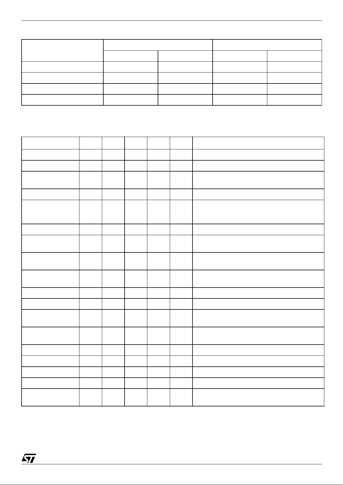
Table 1. Product Range (Note 1)
Note: 1. All product s suppor t: JTAG se rial ISP, MCU para llel ISP, I SP Flash me mory, I SP CPLD, Security features, Power M anagem ent
Unit (PMU), Autom a t ic Power-down (APD )
2. SRAM ma y be backed up usi ng an external battery.
Part Number
Primary Flash
Memory
(8 Sectors)
Secondary
Flash Memory
(4 Sectors)
SRAM
2
I/O Ports
Number of
Macrocells
Serial
ISP
JTAG/
ISC Port
Turbo
Mode
Input Output
PSD813F2 1 Mbit 256 Kbit 16 Kbit 27 24 16 yes yes
PSD813F3 1 Mbit none 16 Kbit 27 24 16 yes yes
PSD813F4 1 Mbit 256 Kbit none 27 24 16 yes yes
PSD813F5 1 Mbit none none 27 24 16 yes yes
PSD833F2 1 Mbit 256 Kbit 64 Kbit 27 24 16 yes yes
PSD834F2 2 Mbit 256 Kbit 64 Kbit 27 24 16 yes yes
PSD853F2 1 Mbit 256 Kbit 256 Kbit 27 24 16 yes yes
PSD854F2 2 Mbit 256 Kbit 256 Kbit 27 24 16 yes yes

9/103
PSD8XXF2/3/4/5
KEY FEATURES
■ A simple interface to 8-bit microcontrollers that
use either multiplexed or non-multiplexed
busses. The bus interface logic uses the control
signals generated by the microcontroller
automatically when the address is decoded and
a READ or WRITE is performed. A partial list of
the MCU families supported include:
– Intel 8031, 80196, 80186, 80C251, and
80386EX
– Motorola 68HC11 , 68HC16, 68HC12, and
683XX
– Philips 8031 and 8051XA
– Zilog Z80 and Z8
■ Internal 1 or 2 Mbit Flash memory. This is the
main Flash memory. It is divided into eight
equal-sized blocks that can be accessed with
user-specified addresses.
■ Internal secondary 256 Kbit Flash boot memory.
It is di vided into f our equal-si zed blo cks that can
be accessed with user-specified addresses.
This seconda ry me mo ry brings th e abilit y to
execute code and update the main Flash
concurrently
.
■ Optional 16, 64 or 256 Kbit SRAM. The SRAM’s
contents can be protected from a power failure
by connecting an external battery.
■ CPLD with 16 Output Micro Cells (OMCs) and
24 Input Micro Cells (IMCs). The CPLD may be
used to efficiently implement a variety of logic
functions for internal and external control.
Examples include state machines, loadable
shift registers, and loadable counters.
■ Decode PLD (DPLD) that decodes address for
selection of internal memory blocks.
■ 27 individually configurable I/O port pins that
can be used for the following functions:
– MCU I/Os
–PLD I/Os
– Latched MCU address output
– Specia l function I/Os.
– 16 of the I/O ports may be configured as
open-drain outputs.
■ Standby current as low as 50 µA for 5 V devices.
■ Built-in JTAG compliant serial port allows full-
chip In-System Programmability (ISP). With it,
you can program a blank device or reprogram a
device in the factory or the field.
■ Internal page register that can be used to
expand the microcontroller address space by a
factor of 256.
■ Internal programmable Power Management
Unit (PMU) that supports a low power mode
called Power Down Mode. The PMU can
automatically detect a lack of microcontroller
activity and put the PSD8XXF into Power-down
mode.
■ Erase/WRITE cycles:
– Flash memory – 100,000 minimum
– PLD – 1,000 minimum
– Data Retention: 15 year minimum (for Main
Flash memory, Boot, PLD and Configuration
bits)
PSD8XXF2/3/4/5
10/103
Figure 3. PSD8XXFX Block Diagram
PROG.
MCU BUS
INTRF.
ADIO
PORT
CNTL0,
CNTL1,
CNTL2
AD0 – AD15
CLKIN
(PD1)
CLKIN
CLKIN
PLD
INPUT
BUS
PROG.
PORT
PORT
A
PROG.
PORT
PORT
B
POWER
MANGMT
UNIT
1 OR 2 MBIT PRIMARY
FLASH MEMORY
8 SECTORS
VSTDBY
PA0 – PA7
PB0 – PB7
PROG.
PORT
PORT
C
PROG.
PORT
PORT
D
PC0 – PC7
PD0 – PD2
ADDRESS/DATA/CONTROL BUS
PORT A ,B & C
3 EXT CS TO PORT D
24 INPUT MACROCELLS
PORT A ,B & C
73
73
256 KBIT SECONDARY
NON-VOLATILE MEMORY
(BOOT OR DATA)
4 SECTORS
256 KBIT BATTERY
BACKUP SRAM
RUNTIME CONTROL
AND I/O REGISTERS
SRAM SELECT
PERIP I/O MODE SELECTS
MACROCELL FEEDBACK OR PORT INPUT
CSIOP
FLASH ISP CPLD
(CPLD)
16 OUTPUT MACROCELLS
FLASH DECODE
PLD
(
DPLD
)
PLD, CONFIGURATION
& FLASH MEMORY
LOADER
JTAG
SERIAL
CHANNEL
(
PC2
)
PAGE
REGISTER
EMBEDDED
ALGORITHM
SECTOR
SELECTS
SECTOR
SELECTS
GLOBAL
CONFIG. &
SECURITY
AI02861E
8

11/103
PSD8XXF2/3/4/5
PSD8XXFX ARCHITECTURAL OVERVIEW
PSD8XXFX devices contain several major func-
tional blocks. Figure 3 shows the architecture of
the PSD8XXFX device family. The functions of
each block are d escribed briefly in the following
sections. Many of the blocks perform multiple
functions and are user configurable.
Memory
Each of the memory blocks is briefly discussed in
the following paragraphs. A more detail ed di scus-
sion can be fo und in the section ent itled “MEM O-
RY BLOCKS“ on page 18.
The 1 Mbit or 2 Mbit (128K x 8, or 256K x 8) Flash
memory is the primary memory of the PSD8XXFX.
It is divided into 8 equally-sized sectors that are in-
dividually selectable.
The optional 256 Kbit (32K x 8) secondary Flash
memory is divided into 4 equally-sized sectors.
Each sector is individually selectable.
The optional SRAM is intended for use as a
scratch-pad memory or as an extension to the
MCU SRAM. If an external battery is connected to
Voltage Stand-by (V
STBY
, PC2), data is retained in
the event of power failure.
Each sector of mem ory can be located in a differ-
ent address space as defined by the user. The ac-
cess times for all memory types includes the
address latching and DPLD decoding time.
Page R egi s te r
The 8-bit Page Register expands the address
range of the MCU by up to 256 times. The paged
address can be used as part of the address space
to access external memory and peripherals, or in-
ternal memory and I/O. The Page Register can
also be used to change the address mapping of
sectors of the Flash memories into different mem-
ory spaces for IAP.
PLDs
The device contains t wo PLDs, the Decode PLD
(DPLD) and the Complex PLD (CPLD), as shown
in Table 2, each op timized for a different function.
The functional partitioning of the PLDs reduces
power consumption, optim izes cost/performance,
and eases design entry.
Table 2. PLD I/O
The DPLD is used to decode addresses and to
generate Sector Select signals for the PSD8XXFX
internal memory and registers. The DPLD has
combinatorial outputs. T he CPLD has 16 Output
Macrocells (OMC) and 3 combinatorial outputs.
The PSD8XXFX also has 24 Input Macrocells
(IMC) that can be configured as inputs to the
PLDs. The PLDs receive their inputs from the PLD
Input Bus and are differentiated by their output
destinations, number of product terms, an d mac-
rocells.
The PLDs consume minimal power. The speed
and power consumption of the PLD i s controlled
by the Turbo bit in PMMR0 and othe r bits in the
PMMR2. These registers are set by the MCU at
run-time. There is a slight penalty to PLD propaga-
tion time when invoking the power management
features.
I/O P or t s
The PSD8XXFX has 27 individually configurable I/
O pins distributed over the four ports (Port A , B, C,
and D). Each I/O pin can be individually configured
for different functions. Ports can be configured as
standard MCU I/O ports, PLD I/O, or latched ad-
dress outputs for MCUs using multiplexed ad-
dress/data buses.
The JTAG pins can be enabled o n Port C for In-
System Programming (ISP).
Ports A and B can a lso be configured as a data
port for a non-multiplexed bus.
MCU Bus Interface
PSD8XXFX interfaces easily with most 8-bit
MCUs that have either multiplexed or non-multi-
plexed address/data b uses. The de vice is config-
ured to respond to the MCU’s control signals,
which are also used as inputs to the PLDs. For ex-
amples, please see the section entitled “MCU Bus
Interface Examples“ on page 43.
Name Inputs Outputs
Product
Terms
Decode PLD (DPLD) 73 17 42
Complex PLD (CPLD) 73 19 140
PSD8XXF2/3/4/5
12/103
JTAG Port
In-System Programming (ISP) can be pe rformed
through the JTAG signals on Port C. This serial in-
terface allows complete programming of the entire
PSD8XXFX device. A bla nk device can be com-
pletely programmed. The JTAG signals (TMS,
TCK, TSTAT
, TERR, TDI, TDO) can be multi-
plexed with other functions on P ort C. Table 3 in-
dicates the JTAG pin assignments.
In-System Programming (ISP)
Using the JTAG signals on Port C, the entire
PSD8XXFX device can be programmed or erased
without the use of the MCU. The primary Flash
memory can also be programmed in-system by
the MCU executing the programming algorithms
out of the secondary memory, or SRAM. The sec-
ondary memory can be programmed the same
way by executing out of the pri mary F lash m emo-
ry. The PLD or other PSD8XXFX Configuration
blocks can be pr ogrammed thro ugh the JTAG port
or a device programmer. Table 4 in dicates which
programming methods can program different func-
tional blocks of the PSD8XXFX.
Power Management Unit (PMU)
The Power Management Unit (PMU) gives the
user control of the power consumption on selected
functional blocks based on system requirements.
The PMU includes an Automatic Power-down
(APD) Unit that turns off device functions during
MCU inactivity. The APD Unit has a Power-down
mode that helps reduce power consump t ion.
The PSD8XXFX al so has some bi ts that are con-
figured at run-time by the MCU to reduce power
consumption of the CPLD. The Turbo bit in
PMMR0 can be reset to 0 and the CPLD latches its
outputs and goes to sleep until the next transit ion
on its inputs.
Additionally, bits in PMMR2 can be set by the
MCU to block signals from entering the CP LD to
reduce power consumption. P lease see the sec-
tion entitled “POWER MANAGEMENT” on page
58 for more details.
Table 3. JTAG SIgnals on Port C
Table 4. Methods of Programming Different Functional Blocks of the PSD8XXFX
Port C Pins JTAG Signal
PC0 TMS
PC1 TCK
PC3 TSTAT
PC4 TERR
PC5 TDI
PC6 TDO
Functional Block JTAG Programming Device Programmer IAP
Primary Flash Memory Yes Yes Yes
Secondary Flash Memory Yes Yes Yes
PLD Array (DPLD and CPLD) Yes Yes No
PSD8XXFX Config urati on Yes Yes No
13/103
PSD8XXF2/3/4/5
DEVELOPMEN T SYST EM
The PSD8XXFX family is supported by PSDsoft
Express, a Windows-based software development
tool. A PSD8XXFX design is quickly and easily
produced in a point and click environment. The de-
signer does not need to enter Hardware Descrip-
tion Language (HDL) equations, unless desired, to
define PSD8XXFX pin functions and memory map
information. The general desig n flow is shown in
Figure 4. PSDsoft Express is available from our
web site (the address is given on the back page of
this data sheet) or other distribution channels.
PSDsoft Express directly supports two low cost
device programmers form ST: PSDpro and
FlashLINK (JTAG). Both of these programmers
may be purchased through your local distributor/
representative, or directly from our web site using
a credit card. The PSD8XXFX is also supported by
third party device programm ers. See our web site
for the current list.
Figure 4. PSDsoft Express Development Tool
PSD Configuration
PSD Fitter
PSD Simulator
PSD Programmer
*.OBJ FILE
PLD DESCRIPTION
CONFIGURE MCU BUS
INTERFACE AND OTHER
PSD ATTRIBUTES
LOGIC SYNTHESIS
AND FITTING
PSDsilos III
DEVICE SIMULATION
(OPTIONAL)
PSDPro, or
FlashLINK (JTAG)
ADDRESS TRANSLATION
AND MEMORY MAPPING
PSDabel
MODIFY ABEL TEMPLATE FILE
OR GENERATE NEW FILE
PSD TOOLS
GENERATE C CODE
SPECIFIC TO PSD
FUNCTIONS
USER'S CHOICE OF
MICROCONTROLLER
COMPILER/LINKER
*.OBJ AND *.SVF
FILES AVAILABLE
FOR 3rd PARTY
PROGRAMMERS
(CONVENTIONAL or
JTAG-ISC)
FIRMWARE
HEX OR S-RECORD
FORMAT
AI04918
PSD8XXF2/3/4/5
14/103
PIN DESCRIPTION
Table 5 describes the signal names and signal
functions of the PSD8XXFX.
Table 5. Pin Description (for the PLCC52 package - Note 1)
Pin Name Pin Type Description
ADIO0-7 30-37 I/O
This is the lower Address/Data port. Connect your MCU address or address/data bus
according to the following rules:
1. If your MCU has a multiplexed address/data bus where the data is multiplexed with the
lower address bits, connect AD0-AD7 to this port.
2. If your MCU does not have a multiplexed address/data bus, or you are using an
80C251 in page mode, connect A0-A7 to this port.
3. If you are using an 80C51XA in burst mode, connect A4/D0 through A11/D7 to this
port.
ALE or AS latches the address. The PSD8XXFX drives data out only if the READ signal is
active and one of the PSD8XXFX functional blocks was selected. The addresses on this
port are passed to the PLDs.
ADIO8-15 39-46 I/O
This is the upper Address/Data port. Connect your MCU address or address/data bus
according to the following rules:
1. If your MCU has a multiplexed address/data bus where the data is multiplexed with the
lower address bits, connect A8-A15 to this port.
2. If your MCU does not have a multiplexed address/data bus, connect A8-A15 to this
port.
3. If you are using an 80C251 in page mode, connect AD8-AD15 to this port.
4. If you are using an 80C51XA in burst mode, connect A12/D8 through A19/D15 to this
port.
ALE or AS latches the address. The PSD8XXFX drives data out only if the READ signal is
active and one of the PSD8XXFX functional blocks was selected. The addresses on this
port are passed to the PLDs.
CNTL0 47 I
The following control signals can be connected to this port, based on your MCU:
1. WR
– active Low Write Strobe input.
2. R_W
– active High READ/active Low write input.
This port is connected to the PLDs. Therefore, these signals can be used in decode and
other logic equations.
CNTL1 50 I
The following control signals can be connected to this port, based on your MCU:
1. RD
– active Low Read Strobe input.
2. E – E clock input.
3. DS
– active Low Data Strobe input.
4. PSEN
– connect PSEN to this port when it is being used as an active Low READ
signal. For example, when the 80C251 outputs more than 16 address bits, PSEN
is
actually the READ signal.
This port is connected to the PLDs. Therefore, these signals can be used in decode and
other logic equations.
CNTL2 49 I
This port can be used to input the PSEN
(Program Select Enable) signal from any MCU
that uses this signal for code exclusively. If your MCU does not output a Program Select
Enable signal, this port can be used as a generic input. This port is connected to the
PLDs.
Reset
48 I
Resets I/O Ports, PLD macrocells and some of the Configuration Registers. Must be Low
at Power-up.
15/103
PSD8XXF2/3/4/5
PA0
PA1
PA2
PA3
PA4
PA5
PA6
PA7
29
28
27
25
24
23
22
21
I/O
These pins make up Port A. These port pins are configurable and can have the following
functions:
1. MCU I/O – write to or read from a standard output or input port.
2. CPLD macrocell (McellAB0-7) outputs.
3. Inputs to the PLDs.
4. Latched address outputs (see Table 6).
5. Address inputs. For example, PA0-3 could be used for A0-A3 when using an 80C51XA
in burst mode.
6. As the data bus inputs D0-D7 for non-multiplexed address/data bus MCUs.
7. D0/A16-D3/A19 in M37702M2 mode.
8. Peripheral I/O mode.
Note: PA0-P A3 can only output CMOS signals with an option for high slew rate. However,
PA4-PA7 can be configured as CMOS or Open Drain Outputs.
PB0
PB1
PB2
PB3
PB4
PB5
PB6
PB7
7
6
5
4
3
2
52
51
I/O
These pins make up Port B. These port pins are configurable and can have the following
functions:
1. MCU I/O – write to or read from a standard output or input port.
2. CPLD macrocell (McellAB0-7 or McellBC0-7) outputs.
3. Inputs to the PLDs.
4. Latched address outputs (see Table 6).
Note: PB0-PB3 can only output CMOS signals with an option for high slew rate. However,
PB4-PB7 can be configured as CMOS or Open Drain Outputs.
PC0 20 I/O
PC0 pin of Port C. This port pin can be configured to have the following functions:
1. MCU I/O – write to or read from a standard output or input port.
2. CPLD macrocell (McellBC0) output.
3. Input to the PLDs.
4. TMS Input
2
for the JTAG Serial Interface.
This pin can be configured as a CMOS or Open Drain output.
PC1 19 I/O
PC1 pin of Port C. This port pin can be configured to have the following functions:
1. MCU I/O – write to or read from a standard output or input port.
2. CPLD macrocell (McellBC1) output.
3. Input to the PLDs.
4. TCK Input
2
for the JTAG Serial Interface.
This pin can be configured as a CMOS or Open Drain output.
PC2 18 I/O
PC2 pin of Port C. This port pin can be configured to have the following functions:
1. MCU I/O – write to or read from a standard output or input port.
2. CPLD macrocell (McellBC2) output.
3. Input to the PLDs.
4. V
STBY
– SRAM stand-by voltage input for SRAM battery backup.
This pin can be configured as a CMOS or Open Drain output.
PC3 17 I/O
PC3 pin of Port C. This port pin can be configured to have the following functions:
1. MCU I/O – write to or read from a standard output or input port.
2. CPLD macrocell (McellBC3) output.
3. Input to the PLDs.
4. TSTAT
output
2
for the JTAG Serial Interface.
5. Ready/Busy
output for parallel In-System Programming (ISP).
This pin can be configured as a CMOS or Open Drain output.
PC4 14 I/O
PC4 pin of Port C. This port pin can be configured to have the following functions:
1. MCU I/O – write to or read from a standard output or input port.
2. CPLD macrocell (McellBC4) output.
3. Input to the PLDs.
4. TERR
output
2
for the JTAG Serial Interface.
5. Battery-on Indicator (VBATON). Goes High when power is being drawn from the
external battery.
This pin can be configured as a CMOS or Open Drain output.
Pin Name Pin Type Description
PSD8XXF2/3/4/5
16/103
Note: 1. The pin numbers in this t abl e are for the PLCC package only. See the package inf ormation, on page 98 onwards, for pin nu mb ers
on other pa ck age types.
2. These functions ca n be m ultiplexe d wi th other functions.
PSD8XXFX REGISTER DESCRIPTION AND ADDRESS OFFSET
Table 7 shows the offset addresses to the
PSD8 XXFX regis ters re lati ve to th e CS IOP ba se
address. The CSIOP space is the 256 bytes of ad-
dress that is allocated by the user to the internal
PSD8XXFX registers. Table 7 provides brief de-
scriptions of the registers in CSIOP space. The fol-
lowing section gives a more detailed description.
PC5 13 I/O
PC5 pin of Port C. This port pin can be configured to have the following functions:
1. MCU I/O – write to or read from a standard output or input port.
2. CPLD macrocell (McellBC5) output.
3. Input to the PLDs.
4. TDI input
2
for the JTAG Serial Interface.
This pin can be configured as a CMOS or Open Drain output.
PC6 12 I/O
PC6 pin of Port C. This port pin can be configured to have the following functions:
1. MCU I/O – write to or read from a standard output or input port.
2. CPLD macrocell (McellBC6) output.
3. Input to the PLDs.
4. TDO output
2
for the JTAG Serial Interface.
This pin can be configured as a CMOS or Open Drain output.
PC7 11 I/O
PC7 pin of Port C. This port pin can be configured to have the following functions:
1. MCU I/O – write to or read from a standard output or input port.
2. CPLD macrocell (McellBC7) output.
3. Input to the PLDs.
4. DBE – active Low Data Byte Enable input from 68HC912 type MCUs.
This pin can be configured as a CMOS or Open Drain output.
PD0 10 I/O
PD0 pin of Port D. This port pin can be configured to have the following functions:
1. ALE/AS input latches address output from the MCU.
2. MCU I/O – write or read from a standard output or input port.
3. Input to the PLDs.
4. CPLD output (External Chip Select).
PD1 9 I/O
PD1 pin of Port D. This port pin can be configured to have the following functions:
1. MCU I/O – write to or read from a standard output or input port.
2. Input to the PLDs.
3. CPLD output (External Chip Select).
4. CLKIN – clock input to the CPLD macrocells, the APD Unit’s Power-down counter, and
the CPLD AND Array.
PD2 8 I/O
PD2 pin of Port D. This port pin can be configured to have the following functions:
1. MCU I/O – write to or read from a standard output or input port.
2. Input to the PLDs.
3. CPLD output (External Chip Select).
4. PSD Chip Select Input (CSI
). When Low, the MCU can access the PSD8XXFX
memory and I/O. When High, the PSD8XXFX memory blocks are disabled to conserve
power.
V
CC
15, 38 Supply Voltage
GND
1, 16,
26
Ground pins
Pin Name Pin Type Description
17/103
PSD8XXF2/3/4/5
Table 6. I/O Port Latched Address Output Assignments (Note1)
Note: 1. See the sect i on entitle d “I/O PORTS”, on page 48, on how to enabl e the Latch ed A ddress Output funct i on.
2. N/A = Not Applicable
Table 7. Register Address Offset
Note: 1. Other registers that are not part of the I/O ports.
MCU
Port A Port B
Port A (3:0) Port A (7:4) Port B (3:0) Port B (7:4)
8051XA (8-bit) N/A Address a7-a4 Address a11-a8 N/A
80C251 (page mode) N/A N/A Address a11-a8 Address a15-a12
All other 8-bit multiplexed Address a3-a0 Address a7-a4 Address a3-a0 Address a7-a4
8-bit non-multiplexed bus N/A N/A Address a3-a0 Address a7-a4
Register Name Port A Port B Port C Port D
Other
1
Description
Data In 00 01 10 11 Reads Port pin as input, MCU I/O input mode
Control 02 03 Selects mode between MCU I/O or Address Out
Data Out 04 05 12 13
Stores data for output to Port pins, MCU I/O output
mode
Direction 06 07 14 15 Configures Port pin as input or output
Drive Select 08 09 16 17
Configures Port pins as either CMOS or Open
Drain on some pins, while selecting high slew rate
on other pins.
Input Macrocell 0A 0B 18 Reads Input Macrocells
Enable Out 0C 0D 1A 1B
Reads the status of the output enable to the I/O
Port driver
Output Macrocells
AB
20 20
READ – reads output of macrocells AB
WRITE – loads macrocell flip-flops
Output Macrocells
BC
21 21
READ – reads output of macrocells BC
WRITE – loads macrocell flip-flops
Mask Macrocells AB 22 22 Blocks writing to the Output Macrocells AB
Mask Macrocells BC 23 23 Blocks writing to the Output Macrocells BC
Primary Flash
Protection
C0 Read only – Primary Flash Sector Protection
Secondary Flash
memory Protection
C2
Read only – PSD8XXFX Security and Secondary
Flash memory Sector Protection
JTAG Enable C7 Enables JTAG Port
PMMR0 B0 Power Management Register 0
PMMR2 B4 Power Management Register 2
Page E0 Page Register
VM E2
Places PSD8XXFX memory areas in Program
and/or Data space on an individual basis.

PSD8XXF2/3/4/5
18/103
DETAILED OPERATION
As shown in Figure 3, the PSD8XXFX cons i sts of
six major types of functional blocks:
■ Memory Blocks
■ PLD Blocks
■ MCU Bus Interface
■ I/O Ports
■ Power Management Unit (PMU)
■ JTAG Interface
The functions of ea ch block are described i n the
following sections. Many of the blocks perform
multiple functions, and are user configurable.
MEMORY BLOCKS
The PSD8XXFX has the following memory blocks:
– Primary Flash memory
– Optional Secondary Flash memory
– Optio nal SRAM
The Memory Select signals for these blocks origi-
nate from the Decode PLD (DP LD) and are user-
defined in PSDsoft Express.
Primary Flash Memory and Secon dary F lash
memory Description
The primary Flash memory is divided evenly into
eight equal sectors. The secondary Flash memory
is divided into four e qual sectors. Each sect or of
either memory block can be s eparately protected
from Program and Erase cycles.
Flash memory may be erased on a sector-by-sec-
tor basis. Flash sector erasure may be suspended
while data is read from other sectors of the block
and then resumed after reading.
During a Program or Erase cycle in Flash memory,
the status can be output on Ready/Busy
(PC3).
This pin is set up using PSDsoft Express Configu-
ration.
Memory Block Select Signals
The DPLD generates the Select signals fo r all the
internal memory blocks (see the section entitled
“PLDS”, on p age 30 ). Eac h o f the eight sectors of
the primary Flash memory has a Select signal
(FS0-FS7) which can contain up to three prod uct
terms. Each of the four sectors of the secondary
Flash memory has a Select signal (CSBOOT0-
CSBOOT3) which can contain up to three product
terms. Having three product terms for each Select
signal allows a given sector to be mapped in differ-
ent areas of system memory. When using a MCU
with separate Program and Data space, these
flexible Select signals allow dynamic re-mapping
of sectors from one memory space to the other.
Ready/Busy
(PC3). This signal can be used to
output the Ready/Busy
status of the PSD8XXF X.
The output on Ready/Busy
(PC3) is a 0 (Busy)
when Flash memory is being written to,
or
when
Flash memory is being erased. The output is a 1
(Ready) when no WRITE or Erase cycle is in
progress.
Memory Operation . The primary Flash memory
and secondary Flash memory are addressed
through the MCU Bus Interface. The MCU can ac-
cess these memories in one of two ways:
■ The MCU can execute a typical bus WRITE or
READ
operation
just as it would if accessing a
RAM or ROM device using standard bus cycles.
■ The MCU can execute a specific instruction that
consists of several WRITE and READ
operations. This involves writing specific data
patterns to special addresses within the Flash
memory to invoke an embedded algorithm.
These instructions are summarized in Table 8.
Typically, the MCU can read Flash memory using
READ operations, just as it would read a ROM de-
vice. However, Flash memory can only be altered
using specific Erase and Program instructions. For
example, the MCU cannot write a single by te di-
rectly to Flash memory as it would write a byte to
RAM. To program a byte into Flash memory, t he
MCU must execute a Program instruction, then
test the status of the Program cycle. This status
test is achieved by a READ operation or polling
Ready/Busy
(PC3).
Flash memory can also be read by using special
instructions to retrieve particular Flash devi ce in-
formation (sector protect status and ID).
19/103
PSD8XXF2/3/4/5
Table 8. Instructions
Note: 1. All bus cyc l es are WRITE bus cycles, except the ones with the “READ” label
2. All values are in hexadecimal:
X = Don’t Care. Addresses of the form X XXXh, in this table, must be even addres ses
RA = Address of the memory l ocation to be read
RD = Data re ad from loca ti on RA during t he READ cyc le
PA = Address of the memory location to be programmed. Addresses are latched on the falling edge of Write Strobe (WR
, CNTL0).
PA is an even address fo r P SD in word programmin g mode.
PD = Data word to be progr am m ed at location PA. Data is la tc hed on the rising edge of Write Strobe (WR
, CNTL0)
SA = Addr ess of the se ctor to be erased or ve rified. T he Sec tor Sel ect (FS 0-FS7 o r CSB OOT0-CSBO OT3) of the se ctor t o be
erased, or verified, must be Active (High).
3. Sector Se l ect (FS0 to FS7 or CSBOOT0 to C SBOOT3) signals are act i ve High, and ar e defined in PSD soft Expre ss .
4. Only address bits A11-A0 are used in instruction decoding.
5. No Unloc k or instruction cycles are required when the devic e i s in the READ Mode
6. The Reset instruction is required to return to the READ Mode after reading the Flash ID, or after reading the Sector Protection Sta-
tus, or if the Er ror Flag (DQ5/DQ13) bit goes High.
7. Additi onal sectors to be erased must be written at the end of t he Sector Erase i nstructi on within 80µs.
8. The dat a is 00h for an unp rotected sector, and 01h for a protec ted sector. In the fourth c ycle, the Sec tor Select i s active, and
(A1,A0)= (1,0)
9. The Unlock Bypass instruction is required prior to the Unlock Bypass Program instruction.
10. The Unlock Bypas s Reset Flas h i nstructi on is requi red to return to readi ng memory data when t he device is i n the Unloc k Bypass
mode.
11. The system may perform READ and Program cycles in non-erasing sectors, read the Flash ID or read the Sector Protection Status
when in the S uspend Sector Erase mo de. T he Suspend Sector Erase instruction is valid only during a Secto r E rase cycle.
12. The Resume Sector Erase instruction is valid only during the Suspend Sector Erase mode.
13. The MCU can not i nvok e these inst ruct ion s whi le exe cutin g cod e from th e sa me Flash mem ory as t hat fo r which th e ins truc tio n is
intended. The MCU must fetch, for example, the code from the secondary Flash memory when reading the Sector Protection Status
of th e prima ry Flas h m em o ry.
Instruction
FS0-FS7 or
CSBOOT0-
CSBOOT3
Cycle 1 Cycle 2 Cycle 3 Cycle 4 Cycle 5 Cycle 6 Cycle 7
READ
5
1
“READ”
RD @ RA
Read Main
Flash ID
6
1
AAh@
X555h
55h@
XAAAh
90h@
X555h
Read identifier
(A6,A1,A0 = 0,0,1)
Read Sector
Protection
6,8,13
1
AAh@
X555h
55h@
XAAAh
90h@
X555h
Read identifier
(A6,A1,A0 = 0,1,0)
Program a
Flash Byte
13
1
AAh@
X555h
55h@
XAAAh
A0h@
X555h
PD@ PA
Flash Sector
Erase
7,13
1
AAh@
X555h
55h@
XAAAh
80h@
X555h
AAh@ XAAAh
55h@
XAAAh
30h@
SA
30h
7
@
next SA
Flash Bulk
Erase
13
1
AAh@
X555h
55h@
XAAAh
80h@
X555h
AAh@ XAAAh
55h@
XAAAh
10h@
X555h
Suspend
Sector Erase
11
1
B0h@
XXXXh
Resume
Sector Erase
12
1
30h@
XXXXh
Reset
6
1
F0h@
XXXXh
Unlock Bypass 1
AAh@
X555h
55h@
XAAAh
20h@
X555h
Unlock Bypass
Program
9
1
A0h@
XXXXh
PD@ PA
Unlock Bypass
Reset
10
1
90h@
XXXXh
00h@
XXXXh

PSD8XXF2/3/4/5
20/103
INSTRUCTIONS
An instruction consists of a sequenc e of specific
operations. Each received byte is sequentially de-
coded by the PSD8XXFX and not executed as a
standard WRITE operation. The instruction is exe-
cuted when the correct number of bytes are prop-
erly received and the time between two
consecutive bytes is shorter t han the tim e-out pe-
riod. Some instructions are structured to include
READ operations after the initial WRITE opera-
tions.
The instruction must be followed exactly. A ny in-
valid combination of instruction bytes or time-out
between two consecutive by tes while addressing
Flash memory reset s the device logic into REA D
Mode (Flash memory is read like a ROM device).
The PSD8XXFX supports the instructions summa-
rized in Table 8:
Flash memory:
■ Erase memory by chip or sector
■ Suspend or resume sector erase
■ Program a Byte
■ Reset to READ Mode
■ Read primary Flash Identifier value
■ Read Sector Protection Status
■ Bypass (on the PSD833F2, PSD834F 2,
PSD853F2 and PSD854F2)
These instructions are detailed in Table 8. F or ef-
ficient decoding of the instructions, the first two
bytes of an instruct ion are the coded cycles and
are followed by an instruction byte or confirmation
byte. The coded cycles consist of writing the data
AAh to address X555h during the first cycle and
data 55h to address XAAAh during the second cy-
cle. Address signals A15-A12 are Do n’t Care dur-
ing the instruction WRITE cycles. However, the
appropriate Sector Select (FS0-FS7 or
CSBOOT0-CSBOOT3 ) m ust be selected.
The primary and secondary Flash memories have
the same instruction set (except for Read Primary
Flash Identifier). The Sector Select signals deter-
mine which Flash memory is to receive and exe-
cute the instruction. The primary Flash memory is
selected if any one of Sector Select (FS0-FS7) is
High, and the secondary Flash memory is selected
if any one of Sector Select (CSBOOT0-
CSBOOT3) is High.
Power-down Instruction and Power-up Mode
Power-up Mode. The PSD8XXFX internal logic
is reset upon Power-up to the READ Mode. Sector
Select (FS0-FS7 and CSBOOT0-CSBOOT3)
must be held Low, and Write Strobe (WR
, CNTL0)
High, during Power-up for maximum security of
the data contents and to remove the poss ibility of
a byte being written on the first edge of Write
Strobe (WR
, CNTL0). Any WRITE cycle initiation
is locked when V
CC
is below V
LKO
.
READ
Under typical conditions, the MCU may read t he
primary Flash memory or the secondary Flash
memory using READ operations just as it would a
ROM or RAM device. Alternately, the MCU may
use READ operations to ob tain status inform at ion
about a Program or Erase cycle that is currently in
progress. Lastly, the MCU may use instructions to
read special data from these memory blocks. The
following sections describe these READ functions.
Read Memory Contents. Primary Flash memor y
and secondary Flash memory are placed in the
READ Mode after Power-up, chip reset, or a Reset
Flash instruction (see Table 8). The MCU can read
the memory contents of the primary Flash memory
or the secondary Flash memory by using RE AD
operations any time the READ operation is not
part of an instruction.
Read Primary Flash Identifier. The primary
Flash memory identifier is read with an instruction
composed of 4 operations: 3 specific WRITE oper-
ations and a RE AD operation (see Table 8). Dur-
ing the READ operation, address bits A6, A1, and
A0 must be 0,0,1, respectivel y, and the appropri-
ate Sector Select (FS0-FS7) must be High. The
identifier for the PSD813F2/3/4/5 is E4h, and for
the PSD83xF2 or PSD85xF2 it is E7h.
Read Memory Sector Protection Status. The
primary Flash memory Sector Protection Status is
read with an instruction composed of 4 operations:
3 specific WRITE operations and a READ opera-
tion (see Table 8). During the READ operation, ad-
dress bits A6, A1, and A0 must be 0,1,0,
respectively, while Sector Select (FS0-FS7 or
CSBOOT0-CSBOOT3) designates the Flash
memory sector whose protection has to be veri-
fied. The READ operation produces 01h if the
Flash memory sector is protected, or 00h if the
sector is not protected.
The sector protection status for all NVM blocks
(primary Flash memory or secondary Flash mem-
ory) can also b e read by the M CU accessing the
Flash Protection registers in PSD I/O space. See
the section entitled “Flash Memory Sector Pro-
tect”, on page 25, for register definitions.

21/103
PSD8XXF2/3/4/5
Reading the Erase/Program Status Bits. The
PSD8XXFX provides several status bits to be
used by the MCU to confirm th e completion of an
Erase or Program cycle of Flash memory. These
status bits minimize the time that the M CU spends
performing these tasks and are defined in Table 9.
The status bits can be read as many times as
needed.
For Flash memory, the MCU can perform a READ
operation to obtain these status bits while an
Erase or Program instruction is being executed by
the embedded algo rithm. See the section ent itled
“Programming Flash Memory”, on page 22, for de-
tails.
Data Polling Flag (DQ7). When erasing or pro-
gramming in Flash memory, the Data Polling Flag
(DQ7) bit outputs the compl em ent of the bit bei ng
entered for programming/writing on the DQ7 bit.
Once the Program instruction or the WRITE oper-
ation is completed, the true logic value i s read on
the Data Polling Flag (DQ7) bit (in a READ opera-
tion).
■ Data Polling is effective after the fourth WRITE
pulse (for a Program instruction) or after the
sixth WRITE pulse (for an Erase instruction). It
must be performed at the address being
programmed or at an address within the Flash
memory sector being erased.
■ During an Erase cycle, the Data Pollin g Flag
(DQ7) bit outputs a 0. After completion of the
cycle, the Data Polling Flag (DQ7) bit outputs
the last bit programmed (it is a 1 after erasing).
■ If the byte to be programmed is in a protected
Flash memory sector, the instruction is ignored.
■ If all the Flash memory sectors to be erased are
protected, the Data Po lling Flag (DQ7) b it is
reset to 0 for about 100µs, and then returns to
the previous addressed byte. No erasure is
performed.
Toggle Fla g (D Q6) . The PSD8XXFX offers an-
ot her wa y f or de t er m in in g wh en t h e F lash memory
Program cycle is completed. During the internal
WRITE operation and when either the FS0-FS7 or
CSBOOT0-CSBOOT3 is true, the Toggle Flag
(DQ6) bit toggles from 0 to 1 and 1 to 0 on subse-
quent attempts to read any byte of the memory.
When the internal cycle is complete, the toggling
stops and the data read on the Data Bus D0-D7 is
the addressed memory byte. The device is now
accessible for a new READ or WRITE operation.
The cycle is finished when two successive READs
yield the same output data.
■ The Toggle Flag (DQ6) bit is effective after the
fourth WRITE pulse (for a Program instruction)
or after the sixth WRITE pulse (for an Erase
instruction).
■ If the byte to be programmed belongs to a
protected Flash memory sector, the instruction
is ignored.
■ If all the Flash memory sectors selected for
erasure are protected, the Toggle Flag (DQ6) bit
toggles to 0 for about 100µs and then returns to
the previous addressed byte.
Error Flag (DQ5). During a normal Program or
Erase cycle, the Error Flag (DQ5) bit is to 0. This
bit is set to 1 when there is a failure during Flash
memory Byte Program, Sector Erase, or Bulk
Erase cycle.
In the case of Flash memory programming, the Er-
ror Flag (DQ5) bit indicates the attempt to program
a Flash memory bit from the programmed state, 0,
to the erased state, 1, which is not valid. The Error
Flag (DQ5) bit may also indicate a Time-out condi-
tion while attempting to program a byte.
In case of an error in a Flash memory Sector Erase
or Byte Prog ram cycle, th e Flash memory sector i n
which the error occurred or to which the pro-
grammed byte bel ongs must no longer be used.
Other Flash memory sectors may still be used.
The Error Flag (DQ5) bit is reset after a Reset
Flash instruction.
Erase Time-out Flag (DQ3). The Erase Time-
out Flag (DQ3) bit reflects the time-out period al-
lowed between two consecutive S ector Erase in-
structions. The Erase Time-out Flag (DQ3) bit is
reset to 0 after a Sector Erase cycle for a time pe-
riod of 100µs + 20% unless an additional Sector
Erase instruction is decoded. After this time peri-
od, or when the additional Sector Erase instruction
is decoded, the Eras e Time-out Flag (DQ3) bit is
set to 1.
Table 9. Status Bit
Note: 1. X = Not guaranteed value , c an be read either 1 or 0.
2. DQ7-DQ0 represent the Data Bus bits, D7-D0.
3. FS0-FS 7 and CSBOO T 0-CSBOOT 3 are active High.
Functional Block
FS0-FS7/CSBO OT0-
CSBOOT3
DQ7 DQ6 DQ5 DQ4 DQ3 DQ2 DQ1 DQ0
Flash Memory
V
IH
Data
Polling
Toggle
Flag
Error
Flag
X
Erase
Time-
out
XXX

PSD8XXF2/3/4/5
22/103
Programming Flash Memory
Flash memory must be erased prior to being pro-
grammed. A byte of Flash memory is erased to all
1s (FFh), and is programmed by setting selected
bits to 0. The MCU may erase Fl ash memory all at
once or by-sector, but not byte-by-byte. Howe ve r,
the MCU may program Flash memory byte-by-
byte.
The primary and secondary Flash memories re-
quire the MCU to send an instruction to program a
byte or to erase sectors (see Table 8).
Once the MCU issues a Flash memory Program or
Erase instruction, it must check for the status bits
for completion. The embedded algorithms that are
invoked inside the PSD8XXFX support several
means to provide status to the MCU. Status may
be checked using any of three methods: Data Poll-
ing, Data Toggle, or Ready/Busy
(PC3).
Data Polling. Polling on the Data Polling Flag
(DQ7) bit is a method of checking whether a P ro-
gram or Erase cycle is in progress or has complet-
ed. Figure 5 shows the Data Polling algorithm.
When the MCU i ssues a Program i nstruction, the
embedded algorithm within the PSD8XXFX be-
gins. The MCU then reads the location of the byte
to be programmed in Flash memory to check sta-
tus. The Data Polling Flag (DQ7) bit of this location
becomes the complement of b7 of the original data
byte to be programmed. The MCU continues to
poll this location, comparing the Dat a P olling Fl ag
(DQ7) bit and monitoring the Error Flag (DQ5) bit.
When the Data Polling Flag (DQ7) bit matches b7
of the original data, and the E rror Flag (DQ5) bit
remains 0, the embedded algorithm is complete. If
the Error Flag (DQ5) bit is 1, the MCU should test
the Data Polling Flag (DQ7) bit again since the
Data Polling Flag (DQ7) bit may have changed si-
multaneously with the Error Flag (DQ5) bit (see
Figure 5).
The Error Flag (DQ5) bit is set if either an internal
time-out occurred while the embedded algorithm
attempted to program the byte or if the MCU at-
tempted to program a 1 to a bit that was not erased
(not erased is logic 0).
It is suggested (as with all Flash memories) to read
the location again after the embedded program-
ming algorithm has completed, to compare the
byte that was written to the Flash memory with the
byte that was intended to be written.
When using the Data Polling method during an
Erase cycle, Figure 5 still applies. However, the
Data Polling Flag (DQ7) bit is 0 until the Erase cy-
cle is complete. A 1 on the Error Flag (DQ5) bit in-
dicates a time-out condition on the Erase cycle; a
0 indicates no error. The MCU can read any loca-
tion within the sector being erased to get the Data
Polling Flag (DQ7) bit and the Error Flag (DQ5) bit.
PSDsoft Express generates ANSI C code func-
tions which implement these Data Polling algo-
rithms.
Figure 5. Dat a Polling Flo wchart
READ DQ5 & DQ7
at VALID ADDRESS
START
READ DQ7
FAIL PASS
AI01369B
DQ7
=
DATA
YES
NO
YES
NO
DQ5
= 1
DQ7
=
DATA
YES
NO
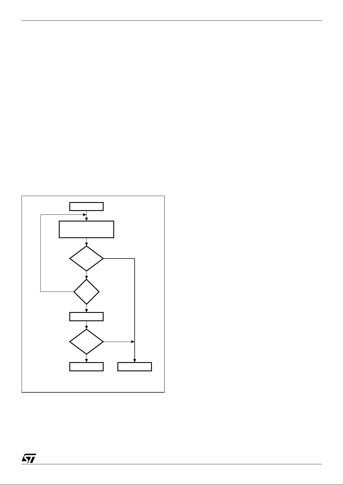
23/103
PSD8XXF2/3/4/5
Data Toggle . Checking the Toggle Flag (DQ6) bit
is a method of determining wh ether a Program or
Erase cycle is in progress or has completed. Fig-
ure 6 shows the Data Toggle algorithm.
When the MCU i ssues a Program instruction, the
embedded algorithm within the PSD8XXFX be-
gins. The MCU then reads the location of the byte
to be programmed in Flash memory to check sta-
tus. The Toggle Flag (DQ6) bit of this location tog-
gles each time the MCU reads this locat ion until
the embedded algorithm is complete. The MCU
continues to read this location, chec king the Tog-
gle Flag (DQ6) bit and monitoring the Error Flag
(DQ5) bit. When the Toggle Flag (DQ6) bi t stops
toggling (two consecutive reads yield the same
value), and the Error Flag (DQ5) bit remains 0, the
embedded algorithm is complete. If the Error Flag
(DQ5) bit is 1, the MCU should test the Toggle
Flag (DQ6) bit again, since the Toggle Flag (DQ6)
bit may have changed simultaneously with the Er-
ror Flag (DQ5) bit (see Figure 6).
Figure 6. Dat a Toggle Flowchart
The Error Flag (DQ5) bit is set if either an internal
time-out occurred while the embedded algorithm
attempted to program the byte, or if the MCU at-
tempted to program a 1 to a bit that was not erased
(not erased is logic 0).
It is suggested (as with all Flash memories) to read
the location again after the embedded program-
ming algorithm has completed, to compare the
byte that was written to Flash memory with the
byte that was intended to be written.
When using the Data Toggle method after an
Erase cycle, Figure 6 still applies. the Toggle Flag
(DQ6) bit toggles until the Erase cycle is complete.
A 1 on the Error Flag (DQ5) bit indicates a time-out
condition on the Erase cycle; a 0 indicates no er-
ror. The MCU can read any location within the sec-
tor being erased to get the Toggle Fla g (DQ6) bit
and the Error Flag (DQ5) bit.
PSDsoft Express generates ANSI C code func-
tions which implement these Data T oggling algo-
rithms.
Unlock Bypass (PSD833F2x, PSD834F2x,
PSD853F2x, PSD854F2x). The Unlock Bypass
instructions allow the system to program bytes to
the Flash memories faster than using the standard
Program instruction. The Unlock Bypass mode is
entered by fi rst ini tiati ng two Unl ock cycle s. This is
followed by a third WRITE cycle containing the Un-
lock Bypass code, 20h (as shown in Table 8).
The Flash memory then enters the Unlock Bypass
mode. A two-cycle Unlock Bypass Program in-
struction is all that is required t o program in this
mode. The first cycle in this instruction contains
the Unlock Bypass Program code, A0h. The sec-
ond cycle contains the program address and data.
Additional data is programm ed in the same man-
ner. These instructions dispense with the initial
two Unlock cycles required in the standard Pro-
gram instruction, resulting in faster total Flash
memory programming.
During the Unlock Bypass mode, only the Unlock
Bypass Program and Unlock Bypass Reset Flash
instructions are valid.
To exit the Un l o ck Bypass mode, the system mus t
issue the two -cycle Un lock Bypass Reset F lash in-
struction. The first cycle must contain the data
90h; the second cycle the data 00h. Addresses are
Don’t Care for both cycles. The Flash memory
then returns to READ Mode.
READ
DQ5 & DQ6
START
READ DQ6
FAIL PASS
AI01370B
DQ6
=
TOGGLE
NO
NO
YES
YES
DQ5
= 1
NO
YES
DQ6
=
TOGGLE

PSD8XXF2/3/4/5
24/103
Erasing Flash Memory
Flash Bulk Erase. The Flash Bulk E rase instruc-
tion uses six WRITE operations followed by a
READ operation of the status register, as de-
scribed in Table 8. If any byte of the Bulk Er ase in-
struction is wrong, the Bulk Erase instruction
aborts and the device is reset t o the Read Flash
memory status.
During a Bulk Erase, the memory status may be
checked by reading the Error Flag (DQ5) bit, the
Toggle Flag (DQ 6) bit, and the Data Polling Flag
(DQ7) bit, as detailed in the section entitled “Pro-
gramming Flash Memory”, on page 22. The Error
Flag (DQ5) bit returns a 1 if there has been an
Erase Failure (maximum number of Erase cycles
have been executed).
It is not necessary to program the memory with
00h because the PSD8X XFX automatically does
this before erasing to 0FFh.
During execution of the Bulk Erase instruction, the
Flash memory does not accept any instructions.
Flash Sector Erase. The Sector Erase instruc-
tion uses six WRITE operations, as descr ibed in
Table 8. Additional Flash Sector Erase codes and
Flash memory sector addresses can be written
subsequently to erase other Flash memory sec-
tors in parallel, without further coded cycles, if the
additional bytes are transmitted in a shorter time
than the time-out period of about 100µs. The input
of a new Sector Erase code restarts the time-out
period.
The status of the internal timer can be m onitored
through the level of the Erase Time-out Flag (DQ3)
bit. If the Erase Time-out Flag (DQ3) bit is 0, the
Sector Erase instruction has been received and
the time-out period is counting. If the E rase Time-
out Flag (DQ3) bit is 1, the time-out period has ex-
pired and the PSD8XXFX is busy erasing the
Flash memory sector(s). Before and during Erase
time-out, any instruction other than Suspend Sec-
tor Erase and Resume Sector Erase instructions
abort the cycle that is currently in progress, and re-
set the device to READ Mode. It is not necessary
to program the Flash m emory sector with 00 h as
the PSD8XXFX does this automatically before
erasing (byte = FFh).
During a Sector Erase, the memory status may be
checked by reading the Error Flag (DQ5) bit, the
Toggle Flag (DQ 6) bit, and the Data Polling Flag
(DQ7) bit, as detailed in the section entitled “Pro-
gramming Flash Memory”, on page 22.
During execution of the Erase cycle, the Flash
memory accepts only Reset and Suspend Sector
Erase instructions. Erasure of one Flash memory
sector may be suspended, in order to read data
from another Flash memory se ctor, and then re-
sume d.
Suspend Sector Erase. When a Sector Erase
cycle is in progress, the Suspend Sector Erase in-
struction can be used to suspend the cycle by writ-
ing 0B0h to any address when an appropriate
Sector Se lect (F S0-FS7 o r CSBOOT0- CSBOOT3)
is High. (See Table 8). This allows reading of data
from another Flash memory sector after the Erase
cycle has been suspended. Suspend Sector
Erase is accepted only during an Er ase cycle and
defaults to READ Mode. A Suspend Sector Erase
instruction executed during an Erase time-out pe-
riod, in addition to suspending the Erase cycle, ter-
minates the time out period.
The Toggle Flag (DQ6) bit stops toggling when the
PSD8XXFX internal logic is suspended . The sta-
tus of this bit must be monitored at an address
within the Flash memory sector being erased. The
Toggle Flag (DQ6) bit stops toggling between
0.1 µ s a nd 15 µs a fter the Suspend S ector Erase
instruction has been executed. The PSD8XXFX is
then automatically set to READ Mode.
If an Suspend Sector Erase instruction was exe-
cuted, the following rules apply:
– Attempting to read from a Flash memory sector
that was being erased outputs invalid data.
– Reading from a Flash sector that was
not
being
erased is valid.
– The Flash memory
cannot
be programmed, and
only responds to Resume Sector Erase and
Reset Flash instructions (READ is an operation
and is allowed).
– If a Reset Flash instruction is received, data in
the Flash memory sector that was being erased
is invalid .
Resume Sector Erase. If a Suspend Sector
Erase instruction was previously executed, the
erase cycle may be resumed with this instruction.
The Resume Sector E rase instruction consists of
writing 030h to any address while an appropriate
Sector Se lect (F S0-FS7 o r CSBOOT0- CSBOOT3)
is High. (See Table 8.)
25/103
PSD8XXF2/3/4/5
Specific Features
Flash Memory Sector Protect. Each primary
and secondary Flash memory sector can be sepa-
rately protected against Program and Erase cy-
cles. Sector Protection provides additional data
security because it disables all Program or Erase
cycles. This mode can be activated through the
JTAG Port or a Device Programmer.
Sector protection can be selec ted for each sector
using the PSDsoft Express Configuration pro-
gram. This automatically protects selected sectors
when the device is programmed through the JTAG
Port or a Device Programmer. Flash memory sec-
tors can be unprotecte d to allow updating of t heir
contents using the JTAG Port or a Device Pro-
grammer. The MCU can read (but cannot change)
the sector protection bits.
Any attempt to program or erase a protected Flash
memory sector is ignored by the device. The Verify
operation results in a READ of the protected data.
This allows a guarantee of the retention of the Pro-
tection status.
The sector protection status can be read by the
MCU through the Flash memory protection and
PSD/EE protection registers (in the CSIOP block).
See Table 10 and Table 11.
Table 10. Sector Protection/Security Bit Definition – Flash Protection Register
Note: 1. Bit De fi nitions:
Sec<i>_Prot 1 = Primary Flash memory or secondary Flash memory Sector <i> is write protected.
Sec<i>_Pr ot 0 = Primary Flash mem ory or secondary Flash mem ory Sector <i> is not write protected.
Table 11. Sector Protection/Security Bit Definition – PSD/EE Protection Register
Note: 1. Bit De fi nitions:
Sec<i>_Prot 1 = Secondary Flash memory Sector <i> is write protected.
Sec<i>_Pr ot 0 = Secondary Flash memory Sector <i> is not write protected.
Security_Bit 0 = Security Bit in device has not been set.
1 = Security B i t in device has been set.
Reset Flash. The Reset Flash instruction con-
sists of one WRITE cycle (see Table 8). It can also
be optionally preceded by the standard two
WRITE decoding cycles (writing AAh to 555h and
55h to AAAh). It must be executed after:
– Reading the Flash Protection Status or Flash ID
– An Error condition has occurred (and the device
has set the Error Flag (DQ5) bit to 1) during a
Flash memory Program or Erase cycle.
On the PSD813F2 /3/4/5, the Reset Fla sh instruc-
tion puts the Flash memory back into normal
READ Mode. It ma y take the Flash memory up t o
a few milliseconds to complete the Reset cycle.
The Reset Flash instruction is ignored when it is is-
sued during a Pr ogram o r Bulk E ras e cycle of t he
Flash memory. The Reset Flash instruction aborts
any on-going Sector Erase cycle, and returns the
Flash memory to the normal READ Mode within a
few millis e co n ds .
On the PSD83xF2 or PSD85xF2, t he Reset Flash
instruction puts the Flash m emory back into nor-
mal READ Mode. If an Error condition has oc-
curred (and the device has set the Error Flag
(DQ5) bit to 1) the Flash m emory is p ut back into
normal READ Mode within 25 µs of the Reset
Flash instruction having been issued. The Reset
Flash instruction is ignored when it is issued dur-
ing a Program or Bulk Erase cycle of the Flash
memory. The Reset F lash instruction aborts any
on-going Sector Erase cycle, and returns the
Flash memory to the normal READ Mode within
25 µs.
Reset (RESET
) Signal (on the PSD83xF2 and
PSD85 xF2). A pulse on Reset (RESET
) aborts
any cycle that is in progress, and resets the Flash
memory to the READ Mode. When the reset oc-
curs during a Program or Erase cycle, the Flash
memory takes up to 25 µs to return to the READ
Mode. It is recommended that the Reset (RESET
)
pulse (except for Power On Reset, as described
on page 63) be at least 25µs so that the Flash
memory is always ready for the MCU to fetch the
bootstrap instructions after the Reset cycle is com-
plete.
Bit 7 Bit 6 Bit 5 Bit 4 Bit 3 Bit 2 Bit 1 Bit 0
Sec7_Prot Sec6_Prot Sec5_Prot Sec4_Prot Sec3_Prot Sec2_Prot Sec1_Prot Sec0_Prot
Bit 7 Bit 6 Bit 5 Bit 4 Bit 3 Bit 2 Bit 1 Bit 0
Security_Bit not used not used not used Sec3_Prot Sec2_Prot Sec1_Prot Sec0_Prot

PSD8XXF2/3/4/5
26/103
SRAM
The SRAM is enab led when SRAM Select (RS0)
from the DPLD is High. SRAM Select (RS0) can
contain up to two prod uct terms, allow ing flexible
memory ma pping.
The SRAM can be backed up using an external
battery. The external battery should be connected
to Voltage Stand-by (V
STBY
, PC2). If you have an
external battery connected to the PSD8XXFX, the
contents of the SRAM are retained i n the event of
a power loss. The contents of the SRAM are re-
tained so long as the battery voltage remains at
2 V or greater. If the supply voltage falls below the
battery voltage, an internal power switch-over to
the battery occurs.
PC4 can be configured as an output that indicates
when power is being drawn from the ext ernal ba t-
tery. Battery-on Indicator (VBATON, PC 4) is Hi gh
with the supply voltage falls below the battery volt-
age and the battery on Voltage Stand-by (V
STBY
,
PC2) is supplying power to the internal SRAM.
SRAM Select (RS0), Voltage Stand-by (V
STBY
,
PC2) and Battery-on Indicator (VBATON, PC4)
are all configured using PSDsoft Express Configu-
ration.
Sector Select and SRAM Select
Sector Select (FS0-FS7, CSBOOT0-CSBOOT3)
and SRAM Select (RS0) are all outputs of the
DPLD. They are setup by writing equations for
them in PSDabel . The foll owing rules apply to the
equations for these signals:
1. Primary Flash memory and secondary Flash
memory Sector Select signals must
not
be
larger than the physical sector size.
2. Any primary Flash memory sector must
not
be
mapped in the same memory space as another
Flash memory sector.
3. A secondary Flash memory sector must
not
be
mapped in the same memory space as another
secondary Flash memory sector.
4. SRAM, I/O, and Peripheral I/O spaces must
not
overlap.
5. A secondary Flash memory sector
may
overlap
a primary Flash memory sector. In case of
overlap, priority is given to the secondary Flash
memory sector.
6. SRAM, I/O, and Peripheral I/O spaces
may
overlap any other memory sector. Priority is
given to the SRAM, I/O, or Peripheral I/O.
Example. FS0 is valid when the address is in the
range of 8000h to BFFFh, CSBOOT0 is valid from
8000h to 9FFF h, and RS0 i s valid from 8000 h to
87FFh. Any addres s in the range of RS0 always
accesses the SRAM. Any address in the range of
CSBOOT0 greater than 87FFh (and less than
9FFFh) automatically addresses secondary Flash
memory segment 0. Any address greater than
9FFFh accesses the prima ry Flash memory seg-
ment 0. You can see that half of the primary Flash
memory segment 0 and o ne-fourth of secondary
Flash memory segment 0 cannot be accessed in
this example. Also no te that an equ ation that de-
fined FS1 to anywhere in the range of 8000h to
BFFFh would
not
be valid.
Figure 7 shows the priority levels for all memory
components. Any component on a higher level can
overlap and has priority over any component on a
lower level. Components on the same level must
not
overlap. Level one has the highest priority and
level 3 has the lowest.
Figure 7. Priority Level of Memory and I/O
Components
Level 1
SRAM, I/O, or
Peripheral I/O
Level 2
Secondary
Non-Volatile Memory
Highest Priority
Lowest Priority
Level 3
Primary Flash Memory
AI02867D
27/103
PSD8XXF2/3/4/5
Memory Select Configuration for MCUs with
Separate Program and Data Spaces. The 8031
and compatible family of MCUs, which includes
the 80C51, 80C151, 80C251, and 80C51XA, have
separate address spaces for Program memory
(selected using Program Select Enable (PSEN
,
CNTL2)) and Data memory (selected using Read
Strobe (RD
, CNTL1)). Any of the memories within
the PSD8XXFX can reside in either space or both
spaces. This is controlled through manipulation of
the VM register that resides in the CSIOP space.
The VM register is set using PSDsoft Express to
have an initial value. It can subsequently be
changed by the MCU so that memory mapping
can be changed on-the-fly.
For example, you may wish to have SRAM and pri-
mary Flash memory in the Data space at Boot-up,
and secondary Flash memory in the Program
space at Boot-up, and later swap the prima ry and
secondary Flash memories. This is easily done
with the VM register by using PSDsoft Express
Configuration to configure it for Boot-up and hav-
ing the MCU change it when desired. Table 12 de-
scribes the VM Register.
Table 12. VM Register
Configuration Modes for MCUs with Separate
Program and Data Spaces. Separate Space
Modes. Program space is separated from Data
space. For example, Program Select Enable
(PSEN
, CNTL2) is used to access the program
code from the p rimary Flash m emory, whi le Read
Strobe (RD
, CNTL1) is used to access data from
the secondary Flash memory, SRAM and I/O Port
blocks. This configuration requires the VM register
to be set to 0Ch (see Figure 8).
Figure 8. 8031 Memory Modules – Separate S pac e
Bit 7
PIO_EN
Bit 6 Bit 5
Bit 4
Primary
FL_Data
Bit 3
Secondary
EE_Data
Bit 2
Primary
FL_Code
Bit 1
Secondary
EE_Code
Bit 0
SRAM_Code
0 = disable
PIO mode
not used not used
0 = RD
can’t
access
Flash
memory
0 = R
D can’t
access Secondary
Flash memory
0 = PSEN
can’t
access
Flash
memory
0 = PSE
N can’t
access Secondary
Flash memory
0 = PSEN
can’t
access
SRAM
1= enable
PIO mode
not used not used
1 = RD
access
Flash
memory
1 = R
D access
Secondary Flash
memory
1 = PSEN
access
Flash
memory
1 = PSE
N access
Secondary Flash
memory
1 = PSEN
access
SRAM
Primary
Flash
Memory
DPLD
Secondary
Flash
Memory
SRAM
RS0
CSBOOT0-3
FS0-FS7
CS CSCS
OE OE
RD
PSEN
OE
AI02869C
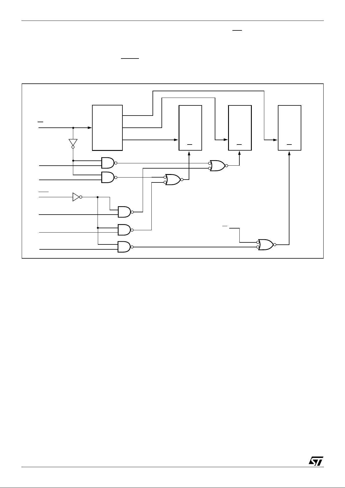
PSD8XXF2/3/4/5
28/103
Combined Space Modes. The Program and
Data spaces are combined into one memory
space that allows the primary Flash memory, sec-
ondary Flash memory, and SRAM to be accessed
by either Program Select Enable (PSEN
, CNTL2)
or Read Strobe (RD
, CNTL1). For example, to
configure the primary Flash mem ory in Combi ned
space, bits b2 and b4 of the VM register are set to
1 (see Figure 9).
Figure 9. 8031 Memory Modules – Combine d Space
Primary
Flash
Memory
DPLD
Secondary
Flash
Memory
SRAM
RS0
CSBOOT0-3
FS0-FS7
RD
CS CSCS
RD
OE OE
VM REG BIT 2
PSEN
VM REG BIT 0
VM REG BIT 1
VM REG BIT 3
VM REG BIT 4
OE
AI02870C
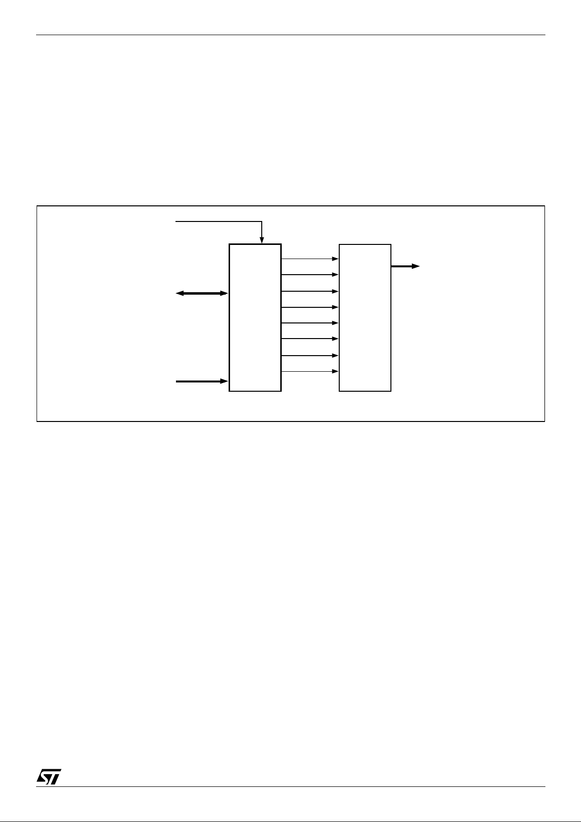
29/103
PSD8XXF2/3/4/5
Page Regi st er
The 8-bit Page Register increases the addressing
capability of the MCU by a factor of up to 256. The
contents of the register can also be read by the
MCU. The outputs of the Page R egister (PGR0-
PGR7) are inputs to the DPLD decoder and can be
included in the Sector Select (FS0-FS7,
CSBOOT0-CSBOOT3 ), and SRAM Select (RS0)
equations.
If memory paging is not needed, or if not all 8 page
register bits are needed for memory paging, then
these bits may be used in the CPLD f or general
logic. See Application Note
AN1154
.
Figure 10 shows the Page Register. The eight flip-
flops in the register are connected to the internal
data bus D0-D7. The MCU can write to or read
from the Page Register. The Page Register can be
accessed at address location CSIOP + E0h.
Figure 10. Page Register
RESET
D0-D7
R/W
D0 Q0
Q1
Q2
Q3
Q4
Q5
Q6
Q7
D1
D2
D3
D4
D5
D6
D7
PAGE
REGISTER
PGR0
PGR1
PGR2
PGR3
DPLD
AND
CPLD
INTERNAL
SELECTS
AND LOGIC
PLD
PGR4
PGR5
PGR6
PGR7
AI02871B
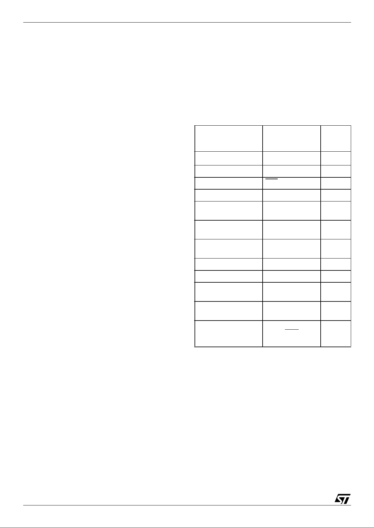
PSD8XXF2/3/4/5
30/103
PLDS
The PLDs bring programmable l ogic functionality
to the PSD8XXFX. After specifying the logic for the
PLDs using the PSDabel tool in PSDsoft Express,
the logic is programmed into the device and avail-
able upon Power-up.
The PSD8XXFX con tains two PLDs: the Decode
PLD (DPLD), and the Co mplex P LD (CP LD). T he
PLDs are briefly discussed in the next few para-
graphs, and in mo re detail in the section entitled
“Decode PLD (DPLD)”, on page 32, and the sec-
tion entitled “Complex PLD (CPLD)”, also on page
33. Figure 11 shows the configuration of the PLDs.
The DPLD performs add ress decoding for S elect
signals for internal components, such as memory,
registers, and I/O ports.
The CPLD can be used for logic functions, such as
loadable counters and shift registers, state ma-
chines, and encoding and decoding logic. These
logic functions can be constructed using the 16
Output Macrocells (OMC), 24 Input Macrocells
(IMC), and the AND Array. The CPLD can also be
used to generate External Chip Select (ECS0-
ECS2) signals.
The AND Array is used to form product terms.
These product terms are specified using PSDabel.
An Input Bus consisting of 73 signals is connected
to the PLDs. The signals are shown in Table 13.
The Turbo Bit in PS D8 X X FX
The PLDs in the PSD8XXFX can minimize power
consumption by switc hing off when i nputs rema in
unchanged for an extended time of about 70ns.
Resetting the Turbo bit to 0 (Bit 3 of PMMR0) au-
tomatically places the PLDs into standby if no in-
puts are changing. Turning the Turbo mode off
increases propagation delays while reducing pow-
er consumption. See the section entitled “POWER
MANAGEMENT”, on page 58, on how to set the
Turbo bit.
Additionally, five bits are available in PMMR2 to
block MCU control signals from entering the PLDs.
This reduces power consumption and can be used
only when these MCU control signals are not used
in PLD logic equations.
Each of the two PLDs has unique characteristics
suited for its applications. They are described in
the following sections.
Table 13. D PL D and C P LD I npu t s
Note: 1. The addres s i nputs are A19-A4 in 80C51XA mode.
Input Source Input Name
Number
of
Signals
MCU Address Bus
1
A15-A0 16
MCU Control Signals CNTL2-CNTL0 3
Reset RST
1
Power-down PDN 1
Port A Input
Macrocells
PA7-PA0 8
Port B Input
Macrocells
PB7-PB0 8
Port C Input
Macrocells
PC7-PC0 8
Port D Inputs PD2-PD0 3
Page Register PGR7-PGR0 8
Macrocell AB
Feedback
MCELLAB.FB7-
FB0
8
Macrocell BC
Feedback
MCELLBC.FB7-
FB0
8
Secondary Flash
memory Program
Status Bit
Ready/Busy
1
 Loading...