


SGS Thomson Microelectronics ST72F652R4T1, ST72F652, ST72F651R6T1, ST72F651AR6T1, ST72F651 Datasheet
...ST7265x
LOW-POWER, FULL-SPEED USB 8-BIT MCU WITH 32K FLASH, 5K RAM, FLASH CARD I/F, TIMER, PWM, ADC, I2C, SPI
■Memories
–Up to 32K of ROM or High Density Flash (HDFlash) program memory with read/write protection
–For HDFlash devices, In-Application Programming (IAP) via USB and In-Circuit programming (ICP)
–Up to 5 Kbytes of RAM with up to 256 bytes stack
■Clock, Reset and Supply Management
–PLL for generating 48 MHz USB clock using a 12 MHz crystal
–Low Voltage Reset (except on E suffix devices)
–Dual supply management: analog voltage detector on the USB power line to enable smart power switching from USB power to battery (on E suffix devices).
–Programmable Internal Voltage Regulator for
Memory cards (2.8V to 3.5V) supplying: Flash Card I/O lines (voltage shifting) Up to 50 mA for Flash card supply
–Clock-out capability
■47 programmable I/O lines
–15 high sink I/Os (8mA @0.6V / 20mA@1.3V)
–5 true open drain outputs
–24 lines programmable as interrupt inputs
■USB (Universal Serial Bus) Interface
–with DMA for full speed bulk applications compliant with USB 12 Mbs specification (version 2.0 compliant)
–On-Chip 3.3V USB voltage regulator and transceivers with software power-down
–5 USB endpoints:
1 control endpoint
2 IN endpoints supporting interrupt and bulk
2 OUT endpoints supporting interrupt and bulk
–Hardware conversion between USB bulk packets and 512-byte blocks
Device Summary
DATASHEET
|
|
|
|
|
|
|
|
|
|
|
|
|
|
|
|
|
|
|
|
|
TQFP64 10x10 |
|
TQFP48 SO34 shrink |
||||
■Mass Storage Interface
– DTC (Data Transfer Coprocessor): Universal
Serial/Parallel communications interface, with software plug-ins for current and future protocol standards:
Compact Flash - Multimedia Card -
Secure Digital Card - SmartMediaCard - Sony Memory Stick - NAND Flash -
ATA Peripherals
■2 Timers
–Configurable Watchdog for system reliability
–16-bit Timer with 2 output compare functions.
■2 Communication Interfaces
–SPI synchronous serial interface
–I2C Single Master Interface up to 400 KHz
■D/A and A/D Peripherals
–PWM/BRM Generator (with 2 10-bit PWM/ BRM outputs)
–8-bit A/D Converter (ADC) with 8 channels
■Instruction Set
–8-bit data manipulation
–63 basic instructions
–17 main addressing modes
–8 x 8 unsigned multiply instruction
–True bit manipulation
■Development Tools
–Full hardware/software development package
Features |
ST72651 |
ST72F651 |
ST72652 |
|
|
|
|
|
|
Program memory |
32K ROM |
32K FLASH |
16K ROM |
|
|
|
|
|
|
User RAM (stack) - bytes |
5K (256) |
512 (256) |
||
|
|
|
||
Peripherals |
USB, DTC, Timer, ADC, SPI, I2C, PWM, WDT |
USB, DTC, WDT |
||
Operating Supply |
Dual 2.7V to 5.5V or |
Dual 3.0V to 5.5V or |
Single 4.0V to 5.5V |
|
4.0V to 5.5V (for USB) |
4.0V to 5.5V (for USB) |
|||
|
|
|||
|
|
|
|
|
Package |
TQFP64 (10 x10) |
TQFP64 (10 x10) / TQFP48 (7x7) / SO34 |
||
|
|
|
|
|
Operating Temperature |
|
0°C to +70°C |
||
|
|
|
|
|
|
|
|
Rev. 2.3 |
|
June 2003 |
|
|
1/166 |
|
This is preliminary information on a new product. Details are subject to change without notice.

Table of Contents
1 INTRODUCTION . . . . . . . . . . . . . . . . . . . . . . . . . . . . . . . . . . . . . . . . . . . . . . . . . . . . . . . . . . . . . . 4 2 PIN DESCRIPTION . . . . . . . . . . . . . . . . . . . . . . . . . . . . . . . . . . . . . . . . . . . . . . . . . . . . . . . . . . . . 7 3 REGISTER & MEMORY MAP . . . . . . . . . . . . . . . . . . . . . . . . . . . . . . . . . . . . . . . . . . . . . . . . . . . 1 8 4 FLASH PROGRAM MEMORY . . . . . . . . . . . . . . . . . . . . . . . . . . . . . . . . . . . . . . . . . . . . . . . . . . 22
4.1 INTRODUCTION . . . . . . . . . . . . . . . . . . . . . . . . . . . . . . . . . . . . . . . . . . . . . . . . . . . . . . . . 22 4.2 MAIN FEATURES . . . . . . . . . . . . . . . . . . . . . . . . . . . . . . . . . . . . . . . . . . . . . . . . . . . . . . . 22 4.3 STRUCTURE . . . . . . . . . . . . . . . . . . . . . . . . . . . . . . . . . . . . . . . . . . . . . . . . . . . . . . . . . . . 22 4.4 PROGRAM MEMORY READ-OUT PROTECTION . . . . . . . . . . . . . . . . . . . . . . . . . . . . . . 22 4.5 ICP (IN-CIRCUIT PROGRAMMING) . . . . . . . . . . . . . . . . . . . . . . . . . . . . . . . . . . . . . . . . . 23 4.6 IAP (IN-APPLICATION PROGRAMMING) . . . . . . . . . . . . . . . . . . . . . . . . . . . . . . . . . . . . . 24 4.7 RELATED DOCUMENTATION . . . . . . . . . . . . . . . . . . . . . . . . . . . . . . . . . . . . . . . . . . . . . 24 4.8 REGISTER DESCRIPTION . . . . . . . . . . . . . . . . . . . . . . . . . . . . . . . . . . . . . . . . . . . . . . . . 24
5 CENTRAL PROCESSING UNIT . . . . . . . . . . . . . . . . . . . . . . . . . . . . . . . . . . . . . . . . . . . . . . . . . |
25 |
|
5.1 |
INTRODUCTION . . . . . . . . . . . . . . . . . . . . . . . . . . . . . . . . . . . . . . . . . . . . . . . . . . . . . . . . |
25 |
5.2 |
MAIN FEATURES . . . . . . . . . . . . . . . . . . . . . . . . . . . . . . . . . . . . . . . . . . . . . . . . . . . . . . . |
25 |
5.3 |
CPU REGISTERS . . . . . . . . . . . . . . . . . . . . . . . . . . . . . . . . . . . . . . . . . . . . . . . . . . . . . . . |
25 |
6 SUPPLY, RESET AND CLOCK MANAGEMENT . . . . . . . . . . . . . . . . . . . . . . . . . . . . . . . . . . . . |
28 |
|
6.1 CLOCK SYSTEM . . . . . . . . . . . . . . . . . . . . . . . . . . . . . . . . . . . . . . . . . . . . . . . . . . . . . . . . 28 6.2 RESET SEQUENCE MANAGER (RSM) . . . . . . . . . . . . . . . . . . . . . . . . . . . . . . . . . . . . . . 29 6.3 LOW VOLTAGE DETECTOR (LVD) . . . . . . . . . . . . . . . . . . . . . . . . . . . . . . . . . . . . . . . . . 32 6.4 POWER SUPPLY MANAGEMENT . . . . . . . . . . . . . . . . . . . . . . . . . . . . . . . . . . . . . . . . . . 33
7 INTERRUPTS . . . . . . . . . . . . . . . . . . . . . . . . . . . . . . . . . . . . . . . . . . . . . . . . . . . . . . . . . . . . . . . |
41 |
7.1 INTRODUCTION . . . . . . . . . . . . . . . . . . . . . . . . . . . . . . . . . . . . . . . . . . . . . . . . . . . . . . . . 41 7.2 MASKING AND PROCESSING FLOW . . . . . . . . . . . . . . . . . . . . . . . . . . . . . . . . . . . . . . . 41 7.3 INTERRUPTS AND LOW POWER MODES . . . . . . . . . . . . . . . . . . . . . . . . . . . . . . . . . . . 43 7.4 CONCURRENT & NESTED MANAGEMENT . . . . . . . . . . . . . . . . . . . . . . . . . . . . . . . . . . 43 7.5 INTERRUPT REGISTER DESCRIPTION . . . . . . . . . . . . . . . . . . . . . . . . . . . . . . . . . . . . . 44
8 POWER SAVING MODES . . . . . . . . . . . . . . . . . . . . . . . . . . . . . . . . . . . . . . . . . . . . . . . . . . . . . |
47 |
|
8.1 |
INTRODUCTION . . . . . . . . . . . . . . . . . . . . . . . . . . . . . . . . . . . . . . . . . . . . . . . . . . . . . . . . |
47 |
8.2 |
WAIT MODE . . . . . . . . . . . . . . . . . . . . . . . . . . . . . . . . . . . . . . . . . . . . . . . . . . . . . . . . . . . |
47 |
- |
HALT MODE |
48 |
8.3 |
||
9 I/O PORTS . . . . . . . . . . . . . . . . . . . . . . . . . . . . . . . . . . . . . . . . . . . . . . . . . . . . . . . . . . . . . . . . . . |
49 |
|
9.1 INTRODUCTION . . . . . . . . . . . . . . . . . . . . . . . . . . . . . . . . . . . . . . . . . . . . . . . . . . . . . . . . 49 9.2 FUNCTIONAL DESCRIPTION . . . . . . . . . . . . . . . . . . . . . . . . . . . . . . . . . . . . . . . . . . . . . . 49 9.3 I/O PORT IMPLEMENTATION . . . . . . . . . . . . . . . . . . . . . . . . . . . . . . . . . . . . . . . . . . . . . . 53 9.4 REGISTER DESCRIPTION . . . . . . . . . . . . . . . . . . . . . . . . . . . . . . . . . . . . . . . . . . . . . . . . 54
10 MISCELLANEOUS REGISTERS . . . . . . . . . . . . . . . . . . . . . . . . . . . . . . . . . . . . . . . . . . . . . . . 56 11 ON-CHIP PERIPHERALS . . . . . . . . . . . . . . . . . . . . . . . . . . . . . . . . . . . . . . . . . . . . . . . . . . . . . 58
11.1 WATCHDOG TIMER (WDG) . . . . . . . . . . . . . . . . . . . . . . . . . . . . . . . . . . . . . . . . . . . . . . . |
58 |
11.2 DATA TRANSFER COPROCESSOR (DTC) . . . . . . . . . . . . . . . . . . . . . . . . . . . . . . . . . . . |
61 |
11.3 USB INTERFACE (USB) . . . . . . . . . . . . . . . . . . . . . . . . . . . . . . . . . . . . . . . . . . . . . . . . . . |
65 |
11.4 16-BIT TIMER . . . . . . . . . . . . . . . . . . . . . . . . . . . . . . . . . . . . . . . . . . . . . . . . . . . . . . . . . . |
80 |
2/166
1

Table of Contents
11.5 PWM/BRM GENERATOR (DAC) . . . . . . . . . . . . . . . . . . . . . . . . . . . . . . . . . . . . . . . . . . . . 92 11.6 SERIAL PERIPHERAL INTERFACE (SPI) . . . . . . . . . . . . . . . . . . . . . . . . . . . . . . . . . . . . 98 11.7 I²C SINGLE MASTER BUS INTERFACE (I2C) . . . . . . . . . . . . . . . . . . . . . . . . . . . . . . . . 109 11.8 8-BIT A/D CONVERTER (ADC) . . . . . . . . . . . . . . . . . . . . . . . . . . . . . . . . . . . . . . . . . . . . 118
12 INSTRUCTION SET . . . . . . . . . . . . . . . . . . . . . . . . . . . . . . . . . . . . . . . . . . . . . . . . . . . . . . . . |
122 |
12.1 CPU ADDRESSING MODES . . . . . . . . . . . . . . . . . . . . . . . . . . . . . . . . . . . . . . . . . . . . . . |
122 |
12.2 INSTRUCTION GROUPS . . . . . . . . . . . . . . . . . . . . . . . . . . . . . . . . . . . . . . . . . . . . . . . . |
125 |
13 ELECTRICAL CHARACTERISTICS . . . . . . . . . . . . . . . . . . . . . . . . . . . . . . . . . . . . . . . . . . . . |
128 |
13.1 PARAMETER CONDITIONS . . . . . . . . . . . . . . . . . . . . . . . . . . . . . . . . . . . . . . . . . . . . . . |
128 |
13.2 ABSOLUTE MAXIMUM RATINGS . . . . . . . . . . . . . . . . . . . . . . . . . . . . . . . . . . . . . . . . . . |
129 |
13.3 OPERATING CONDITIONS . . . . . . . . . . . . . . . . . . . . . . . . . . . . . . . . . . . . . . . . . . . . . . . |
130 |
13.4 SUPPLY CURRENT CHARACTERISTICS . . . . . . . . . . . . . . . . . . . . . . . . . . . . . . . . . . . |
132 |
13.5 CLOCK AND TIMING CHARACTERISTICS . . . . . . . . . . . . . . . . . . . . . . . . . . . . . . . . . . |
135 |
13.6 MEMORY CHARACTERISTICS . . . . . . . . . . . . . . . . . . . . . . . . . . . . . . . . . . . . . . . . . . . |
136 |
13.7 EMC CHARACTERISTICS . . . . . . . . . . . . . . . . . . . . . . . . . . . . . . . . . . . . . . . . . . . . . . . |
137 |
13.8 I/O PORT PIN CHARACTERISTICS . . . . . . . . . . . . . . . . . . . . . . . . . . . . . . . . . . . . . . . . |
142 |
13.9 CONTROL PIN CHARACTERISTICS . . . . . . . . . . . . . . . . . . . . . . . . . . . . . . . . . . . . . . . |
146 |
13.10TIMER PERIPHERAL CHARACTERISTICS . . . . . . . . . . . . . . . . . . . . . . . . . . . . . . . . . |
148 |
13.11COMMUNICATION INTERFACE CHARACTERISTICS . . . . . . . . . . . . . . . . . . . . . . . . |
149 |
13.128-BIT ADC CHARACTERISTICS . . . . . . . . . . . . . . . . . . . . . . . . . . . . . . . . . . . . . . . . . . |
154 |
14 PACKAGE CHARACTERISTICS . . . . . . . . . . . . . . . . . . . . . . . . . . . . . . . . . . . . . . . . . . . . . . |
156 |
14.1 PACKAGE MECHANICAL DATA . . . . . . . . . . . . . . . . . . . . . . . . . . . . . . . . . . . . . . . . . . . |
156 |
15 DEVICE CONFIGURATION AND ORDERING INFORMATION . . . . . . . . . . . . . . . . . . . . . . . |
159 |
15.1 OPTION BYTE . . . . . . . . . . . . . . . . . . . . . . . . . . . . . . . . . . . . . . . . . . . . . . . . . . . . . . . . |
159 |
15.2 DEVICE ORDERING INFORMATION AND TRANSFER OF CUSTOMER CODE . . . . . 160 |
|
15.3 DEVELOPMENT TOOLS . . . . . . . . . . . . . . . . . . . . . . . . . . . . . . . . . . . . . . . . . . . . . . . . . |
162 |
15.4 ST7 APPLICATION NOTES . . . . . . . . . . . . . . . . . . . . . . . . . . . . . . . . . . . . . . . . . . . . . . |
163 |
16 SUMMARY OF CHANGES . . . . . . . . . . . . . . . . . . . . . . . . . . . . . . . . . . . . . . . . . . . . . . . . . . . |
165 |
3/166
1
ST7265x
1 INTRODUCTION
The ST7265x MCU supports volume data exchange with a host (computer or kiosk) via a full speed USB interface. The MCU is capable of handling various transfer protocols, with a particular emphasis on mass storage applications.
ST7265x is compliant with the USB Mass Storage Class specifications, and supports related protocols such as BOT (Bulk Only Transfer) and CBI (Control, Bulk, Interrupt).
It is based on the ST7 standard 8-bit core, with specific peripherals for managing USB full speed data transfer between the host and most types of FLASH media card:
– A full speed USB interface with Serial Interface Engine, and on-chip 3.3V regulator and transceivers.
–A dedicated 24 MHz Data Buffer Manager state machine for handling 512-byte data blocks (this size corresponds to a sector both on computers and FLASH media cards).
–A Data Transfer Coprocessor (DTC), able to handle fast data transfer with external devices. This DTC also computes the CRC or ECC required to handle Mass storage media.
–An Arbitration block gives the ST7 core priority over the USB and DTC when accessing the Data Buffer. In USB mode, the USB interface is serviced before the DTC.
–A FLASH Supply Block able to provide programmable supply voltage and I/O electrical levels to the FLASH media.
Figure 1. USB Data Transfer Block Diagram
USB
SIE
|
|
|
|
|
|
|
|
|
|
|
|
|
|
|
|
|
|
|
|
|
|
|
|
|
|
|
|
|
|
|
|
|
|
|
|
|
|
|
|
|
|
|
|
|
|
|
|
|
|
|
|
|
|
|
|
|
|
|
|
|
|
|
|
USB DATA |
|
|
|
|
|
|
DATA TRANSFER |
||||||
|
|
|
|
|
|
|
|
|
|
|
|
TRANSFER |
|
|
|
|
|
|
|
|
BUFFER |
||||
|
|
|
|
|
|
|
|
|
|
|
|
|
|
|
|
|
|
|
|
||||||
|
|
|
|
|
|
|
|
|
|
|
|
|
|
|
|
|
|
|
|
|
|||||
|
|
|
|
|
|
|
|
|
|
|
|
|
|
|
|
|
|
|
|
|
|
|
|
|
|
|
|
|
|
|
|
|
|
|
|
|
|
|
|
|
|
|
|
|
|
|
|
|
|
512-byte RAM |
|
|
|
|
|
|
|
|
|
|
|
|
|
|
|
|
|
|
|
|
|
|
|
|
|
|
|
|
|
|
|
|
|
|
|
|
|
|
|
|
|
|
|
|
|
|
|
|
|
|
|
|
|
|
|
|
|
|
|
|
|
|
|
|
|
|
|
|
|
|
|
|
|
|
|
|
|
|
|
ST7 CORE |
|
|
|
|
|
|
BUFFER ACCESS |
|
|
|
|
|
|
Buffer |
|
||||||||||
|
|
|
|
|
|
|
|
ARBITRATION |
|
|
|
|
|
|
|
|
|||||||||
|
|
|
|
|
|
|
|
|
|
|
|
|
|
|
|
|
512-byte RAM |
|
|||||||
|
|
|
|
|
|
|
|
|
|
|
|
|
|
|
|
|
|
|
|
|
|
|
|
|
|
|
|
|
|
|
|
|
|
|
|
|
|
|
|
|
|
|
|
|
|
|
|
|
|
|
|
|
|
|
|
|
|
|
|
|
|
|
|
|
|
|
|
|
|
|
|
|
|
|
|
Buffer |
|
|
|
|
|
|
|
|
|
|
|
|
|
|
|
|
|
|
|
|
|
|
|
|
|
|
|
|
|
|
|
|
|
|
|
|
|
|
|
DATA |
|
|
|
|
|
|
|
|
|
||||
|
|
|
|
|
|
|
|
|
|
|
|
|
|
|
|
|
|
|
|
||||||
|
|
|
|
|
|
|
|
|
|
|
TRANSFER |
|
|
|
|
|
|
|
|
|
|||||
|
|
|
|
|
|
||||||||||||||||||||
|
|
|
|
|
|
|
|
|
|
|
|
|
|
|
|
|
|
|
|
||||||
|
|
|
|
|
|
|
|
|
|
COPROCESSOR |
|
|
|
|
|
|
|
|
|
||||||
|
|
|
|
|
|
|
|
|
|
|
|
(DTC) |
|
|
|
|
|
|
|
|
|
||||
|
|
|
|
|
|
|
|
|
|
|
|
|
|
|
|
|
|
|
|
|
|
|
|
|
|
|
|
|
|
|
|
|
|
|
|
|
|
|
|
|
|
|
|
|
|
|
|
|
|
|
|
LEVEL
SHIFTERS
MASS
STORAGE
DEVICE
4/166
1

ST7265x
INTRODUCTION (Cont’d)
In addition to the peripherals for USB full speed data transfer, the ST7265x includes all the necessary features for stand-alone applications with FLASH mass storage.
–Low voltage reset ensuring proper power-on or power-off of the device (not on all products)
–Digital Watchdog
–16-bit Timer with 2 output compare functions (not on all products - see device summary).
–Two 10-bit PWM outputs (not on all products - see device summary)
–Serial Peripheral interface (not on all products - see device summary)
–Fast I2C Single Master interface (not on all products - see device summary)
–8-bit Analog-to-Digital converter (ADC) with 8 multiplexed analog inputs (not on all products - see device summary)
The ST72F65x are the Flash versions of the ST7265x in a TQFP64 package.
The ST7265x are the ROM versions in a TQFP64 package.
Figure 2. Digital Audio Player Application Example in Play Mode
DATA TRANSFER |
|
BUFFER |
|
512-byte RAM |
512-byte RAM |
Buffer |
Buffer |
BUFFER ACCESS
ST7 CORE
ARBITRATION
DATA TRANSFER
COPROCESSOR I2C (DTC)
LEVEL SHIFTERS
|
|
|
|
|
|
|
|
|
|
|
|
|
|
|
|
|
|
|
|
|
|
|
|
|
|
|
|
|
|
MASS |
|
|
|
DIGITAL |
|||||
STORAGE |
|
|
|
||||||
|
|
|
AUDIO DEVICE |
||||||
DEVICE |
|
|
|
||||||
|
|
|
|
|
|
||||
|
|
|
|
|
|
|
|
|
|
5/166
1

ST7265x
INTRODUCTION (Cont’d)
Figure 3. ST7265x Block Diagram
OSCIN |
12MHz |
|
|
|
|
|
|
|
|
|
|
|
|
OSCOUT |
OSC |
|
CLOCK |
|
PORT A |
PA[7:0] |
|
|
|
|
(8 bits) |
||
|
|
|
DIVIDER |
|
|
|
|
48MHz |
|
|
|
|
|
|
|
|
|
|
PB[7:0] |
|
|
PLL |
|
|
|
PORT B |
|
|
|
fCPU |
|
(8 bits) |
||
|
|
|
|
|
||
|
|
|
|
|
|
|
|
|
|
|
|
SPI * |
|
|
|
|
|
|
PORT C |
PC[7:0] |
|
|
|
|
|
(8 bits) |
|
|
|
|
|
|
|
|
|
DATA |
|
|
|
DATA |
|
|
TRANSFER |
ARBITRATION |
|
|
TRANSFER |
|
|
BUFFER |
|
|
COPROCESSOR |
|
|
|
(1280 bytes) |
|
|
|
||
|
|
|
DTC S/W RAM |
|
||
|
|
|
|
|
||
|
|
|
ADDRESS |
(256 Bytes) |
|
|
|
|
|
PORT E |
PE[7:0] |
||
|
|
|
(8 bits) |
|||
|
|
|
|
|||
|
|
|
|
|
||
|
|
|
|
AND |
PWM* |
|
|
|
|
|
|
|
|
USBDP |
|
|
|
DATA |
|
|
USBDM |
USB |
|
|
PORT F |
|
|
USBVCC |
|
|
|
BUS |
|
PF[6:0] |
PD[7:0] |
|
|
|
|
||
|
|
|
I2C* |
(7 bits) |
||
PORT D |
|
|
|
|||
(8 bits) |
|
|
|
|||
|
|
|
|
|
|
|
|
16-BIT TIMER* |
|
|
8-BIT ADC* |
|
|
|
|
|
|
|
|
|
|
WATCHDOG |
|
|
|
VDDF |
|
|
|
|
|
|
FLASH SUPPLY |
|
RESET |
CONTROL |
|
|
|
BLOCK |
VSSF |
|
8-BIT CORE |
|
|
|
POWER SUPPLY |
VDDA |
VPP |
ALU |
|
|
|
REGULATOR |
VSSA |
|
|
|
|
|
|
|
|
LVD* |
|
|
|
|
VDD1,VDD2 |
|
RAM |
|
|
|
DUAL SUPPLY |
VSS1, VSS2 |
|
|
|
|
MANAGER * |
USBVDD |
|
|
(0.5/5 KBytes) |
|
|
|
||
|
|
|
|
USBVSS |
||
|
|
|
|
|
|
|
|
PROGRAM |
|
|
|
|
|
|
MEMORY |
|
|
|
|
|
|
(16/32 Kbytes) |
|
|
|
|
|
* not on all products (refer to Table 1: Device Summary)
6/166
1
ST7265x
2 PIN DESCRIPTION
Figure 4. 34-Pin SO Package Pinout
VSSA |
1 |
34 |
|
VSS2 |
2 |
33 |
|
OSCIN |
3 |
32 |
|
OSCOUT |
4 |
31 |
|
USBVSS |
5 |
30 |
|
USBDM |
6 |
29 |
|
USBDP |
7 |
28 |
|
USBVCC |
8 |
27 |
|
USBVDD |
9 |
26 |
|
VDDF |
|
10 |
ei1 25 |
|
|||
|
|||
VSSF |
|
11 |
24 |
|
|||
|
|||
DTC / PA0 |
|
12 |
23 |
|
|||
DTC / PA1 |
|
13 |
22 |
|
|||
|
|
ei0 |
|
DTC / PA2 |
|
14 |
21 |
|
|||
DTC / PA3 |
|
15 |
20 |
|
|||
MCO / (HS) PC0 |
|
16 |
19 |
|
|||
|
|
ei2 |
ei2 |
DTC / (HS) PC1 |
|
17 |
18 |
|
|
||
|
|
|
|
VDDA
 VDD2
VDD2
PF6 (HS) / ICCDATA
 PF5 (HS) / ICCCLK
RESET
VPP/ICCSEL
PD6
PD5
PD4
PD3
PD2
PD1
PD0
VSS1
VDD1
PC3 (HS) / DTC
 PC2 (HS) / DTC
I/O pin supplied by VDDF / VSSF
(HS) |
high sink capability |
eix |
associated external interrupt vector |
7/166
1
ST7265x
PIN DESCRIPTION (Cont’d)
Figure 5. 48-Pin TQFP Package Pinout
|
|
|
|
OSCOUT |
OSCIN |
V V V V (HS)PF6/ ICCDATA (HS)/ICCCLKPF5 |
RESET |
V PE4 |
PE3/DTC |
|
||||||||||||||||||
|
|
|
|
|
|
|
|
SS2 SSA DDA DD2 |
|
|
ICCSEL |
|
|
|||||||||||||||
|
|
|
|
|
|
|
|
|
|
|
PP/ |
|
|
|||||||||||||||
|
|
|
|
|
||||||||||||||||||||||||
USBVSS |
48 47 46 45 |
44 43 42 41 40 39 38 37 |
PE2 (HS) / DTC |
|||||||||||||||||||||||||
1 |
|
|
|
|
|
|
|
|
|
|
|
|
|
|
|
|
|
|
|
|
|
|
|
36 |
||||
USBDM |
2 |
|
|
|
|
|
|
|
|
|
|
|
|
|
|
|
|
|
|
|
|
|
|
|
35 |
PE1 (HS) / DTC |
||
USBDP |
3 |
|
|
|
|
|
|
|
|
|
|
|
|
|
|
|
|
|
|
|
|
|
|
|
34 |
PE0 (HS) / DTC |
||
USBVCC |
4 |
|
|
|
|
|
|
|
|
|
|
|
|
|
|
|
|
|
|
|
|
|
|
|
33 |
PD7 |
||
USBVDD |
5 |
|
|
|
|
|
|
|
|
|
|
|
|
|
|
|
|
|
|
|
|
|
|
|
32 |
PD6 |
||
VDDF |
|
|
6 |
|
|
|
|
|
|
|
|
|
|
|
|
|
|
|
|
|
|
|
|
|
|
|
31 |
PD5 |
|
|
|
|
|
|
|
|
|
|
|
|
|
|
|
|
|
|
|
|
|
|
|
|
|
||||
|
|
|
|
|
|
|
|
|
|
|
|
|
|
|
|
|
|
|
|
|
|
|
|
|
PD4 |
|||
VSSF |
|
|
7 |
|
|
|
|
|
|
|
|
|
|
|
|
|
|
|
|
|
|
|
|
ei1 |
30 |
|||
|
|
|
|
|
|
|
|
|
|
|
|
|
|
|
|
|
|
|
|
|||||||||
|
|
|
|
|
|
|
|
|
|
|
|
|
|
|
|
|
|
|
|
PD3 |
||||||||
DTC/PB0 |
|
|
8 |
|
|
|
|
|
|
|
|
|
|
|
|
|
|
|
|
|
|
|
|
29 |
||||
|
|
|
|
|
|
|
|
|
|
|
|
|
|
|
|
|
|
|
|
|
|
|
|
|
||||
|
|
|
|
|
|
|
|
|
|
|
|
|
|
|
|
|
|
|
|
|
|
|
||||||
DTC/PB1 |
|
|
9 |
|
|
|
|
|
|
|
|
|
|
|
|
|
|
|
|
|
|
|
|
|
|
|
28 |
PD2 |
|
|
|
|
|
|
|
|
|
|
|
|
|
|
|
|
|
|
|
|
|
|
|
||||||
|
|
|
|
|
|
|
|
|
|
|
|
|
|
|
|
|
|
|
|
|
|
|
||||||
DTC/PB2 |
|
|
10 |
|
|
|
|
|
|
|
|
|
|
|
|
ei0 |
|
|
|
|
|
|
27 |
PD1 |
||||
|
|
|
|
|
|
|
|
|
|
|
|
|
|
|
|
|
|
|
||||||||||
|
|
|
|
|
|
|
|
|
|
|
|
|
|
|
|
|
|
|
||||||||||
DTC/PB3 |
|
|
11 |
|
|
|
|
|
|
|
|
|
|
|
|
|
|
|
|
|
|
26 |
PD0 |
|||||
|
|
|
|
|
|
|
|
|
|
|
|
|
|
|||||||||||||||
DTC/PB4 |
|
12 |
|
|
|
|
|
|
|
|
|
|
|
|
|
|
|
|
|
|
|
|
|
|
25 |
VSS1 |
||
|
|
|
|
|
|
|
|
|
|
|
|
|
|
|
|
|
|
|
|
|
|
|
||||||
|
|
|
|
|
|
|
|
|
|
|
|
|
|
|
|
|
|
|
|
|
|
|
||||||
|
13 14 15 16 17 18 19 20 21 22 23 24 |
|
||||||||||||||||||||||||||
|
|
|
|
|
|
|
|
|
|
|
|
|
|
|
|
|
|
|
|
|
|
|
|
|
|
|
|
|
|
|
|
DTC/PB5 |
DTC/PB6 |
DTC/PB7 /DTCPA0 |
/DTCPA1 /DTCPA2 /DTCPA3 /DTCPA4 |
/DTCPA5 |
/DTCPA6 /DTCPA7 |
V |
|
||||||||||||||||||
|
|
|
|
|
|
|
|
|
|
|
|
|
|
|
|
|
|
|
|
|
|
|
|
|
|
|
DD1 |
|
I/O pin supplied by VDDF / VSSF
(HS) |
high sink capability |
eix |
associated external interrupt vector |
8/166
1
ST7265x
PIN DESCRIPTION (Cont’d)
Figure 6. 64-Pin TQFP Package Pinout
|
|
OSCOUT OSCIN V |
|
|
V (HS)/ICCDATAPF6 |
|
|
PWM1/PE4 |
|
||||||||||||||||||||||||
|
|
V |
V |
(HS)/ICCCLKPF5 |
(HS)PF4/ USBEN AIN1/PF3 AIN0/PF2 (HS)PF1/ SDA (HS)PF0/ SCL RESET V |
|
|||||||||||||||||||||||||||
|
|
|
|
|
|
|
SS2 |
SSA |
DDA |
DD2 |
|
|
|
|
|
|
|
|
|
|
|
|
|
|
/ICCSEL |
|
|
||||||
|
|
|
|
|
|
|
|
|
|
|
|
|
|
|
|
|
|
|
|
|
PP |
|
|
||||||||||
|
|
|
|
||||||||||||||||||||||||||||||
USBVSS |
64 63 62 61 60 59 58 57 56 55 54 53 52 51 50 49 |
PE3 / PWM0 / AIN7 / DTC |
|||||||||||||||||||||||||||||||
1 |
|
|
|
|
|
|
|
|
|
|
|
|
|
|
|
|
|
|
|
|
|
|
|
|
|
|
|
|
|
48 |
|||
USBDM |
2 |
|
|
|
|
|
|
|
|
|
|
|
|
|
|
|
|
|
|
|
|
|
|
|
|
|
|
|
|
|
47 |
PE2 (HS) / AIN6 / DTC |
|
USBDP |
3 |
|
|
|
|
|
|
|
|
|
|
|
|
|
|
|
|
|
|
|
|
|
|
|
|
|
|
|
|
|
46 |
PE1 (HS) / AIN5 / DTC |
|
USBVCC |
4 |
|
|
|
|
|
|
|
|
|
|
|
|
|
|
|
|
|
|
|
|
|
|
|
|
|
|
|
|
|
45 |
PE0 (HS) / AIN4 / DTC |
|
USBVDD |
5 |
|
|
|
|
|
|
|
|
|
|
|
|
|
|
|
|
|
|
|
|
|
|
|
|
|
|
|
|
|
44 |
PD7 / AIN3 |
|
VDDF |
|
6 |
|
|
|
|
|
|
|
|
|
|
|
|
|
|
|
|
|
|
|
|
|
|
|
|
|
|
|
|
|
43 |
PD6 / AIN2 |
|
|
|
|
|
|
|
|
|
|
|
|
|
|
|
|
|
|
|
|
|
|
|
|
||||||||||
|
|
|
|
|
|
|
|
|
|
|
|
|
|
|
|
|
|
|
|
|
|
|
|
||||||||||
VSSF |
|
7 |
|
|
|
|
|
|
|
|
|
|
|
|
|
|
|
|
|
|
|
|
|
|
|
|
|
|
|
|
|
42 |
PD5/OCMP2 |
|
|
|
|
|
|
|
|
|
|
|
|
|
|
|
|
|
|
|
|
|
|
|
|
||||||||||
|
|
|
|
|
|
|
|
|
|
|
|
|
|
|
|
|
|
|
|
|
|
|
|
||||||||||
DTC / PE5 (HS) |
|
8 |
|
|
|
|
|
|
|
|
|
|
|
|
|
|
|
|
|
|
|
|
|
|
|
|
|
|
|
ei1 |
41 |
PD4/OCMP1 |
|
|
|
|
|
|
|
|
|
|
|
|
|
|
|
|
|
|
|
|
|
|
|
||||||||||||
DTC / PE6 (HS) |
|
9 |
|
|
|
|
|
|
|
|
|
|
|
|
|
|
|
|
|
|
|
|
|
|
|
|
|
|
|
40 |
PD3 |
||
|
|
|
|
|
|
|
|
|
|
|
|
|
|
|
|
|
|
|
|
|
|
|
|
|
|
|
|
|
|
||||
|
|
|
|
|
|
|
|
|
|
|
|
|
|
|
|
|
|
|
|
|
|
|
|
||||||||||
DTC / PE7 (HS) |
|
10 |
|
|
|
|
|
|
|
|
|
|
|
|
|
|
|
|
|
|
|
|
|
|
|
|
|
|
|
|
39 |
PD2 |
|
|
|
|
|
|
|
|
|
|
|
|
|
|
|
|
|
|
|
|
|
|
|
|
|
||||||||||
|
|
|
|
|
|
|
|
|
|
|
|
|
|
|
|
|
|
|
|
|
|
|
|
||||||||||
DTC / PB0 |
|
11 |
|
|
|
|
|
|
|
|
|
|
|
|
|
|
|
|
|
|
|
|
|
|
|
|
|
|
|
|
38 |
PD1 |
|
|
|
|
|
|
|
|
|
|
|
|
|
|
|
|
|
|
|
|
|
|
|
|
|
||||||||||
|
|
|
|
|
|
|
|
|
|
|
|
|
|
|
|
|
|
|
|
|
|
|
|
||||||||||
DTC / PB1 |
|
12 |
|
|
|
|
|
|
|
|
|
|
|
|
|
|
|
|
|
|
|
|
|
|
|
|
|
|
|
|
37 |
PD0 |
|
|
|
|
|
|
|
|
|
|
|
|
|
|
|
|
|
|
|
|
|
|
|
|
|
||||||||||
|
|
|
|
|
|
|
|
|
|
|
|
|
|
|
|
|
|
|
|
|
|
|
|
||||||||||
DTC / PB2 |
|
13 |
|
|
|
|
|
|
|
|
|
|
|
|
|
|
|
|
|
|
|
|
|
|
|
|
|
|
|
|
36 |
PC7 |
|
|
|
|
|
|
|
|
|
|
|
|
|
|
|
|
|
|
|
|
|
|
|
|
|
||||||||||
|
|
|
|
|
|
|
|
|
|
|
|
|
|
|
|
|
|
|
|
|
|
|
|
||||||||||
DTC / PB3 |
|
14 |
|
|
|
|
|
|
|
|
|
|
ei0 |
|
|
|
|
|
|
|
|
ei2 |
ei2 |
35 |
PC6 |
||||||||
|
|
|
|
|
|
|
|
|
|
|
|
|
|
||||||||||||||||||||
|
|
|
|
|
|
|
|
|
|
|
|
|
|
||||||||||||||||||||
DTC / PB4 |
|
15 |
|
|
|
|
|
|
|
|
|
|
|
|
|
|
|
|
|
|
|
|
34 |
PC5 |
|||||||||
|
|
|
|
|
|
|
|
|
|
|
|
|
|
|
|
|
|
|
|
|
|
|
|
|
|
|
|
|
|||||
|
|
|
|
|
|
|
|
|
|
|
|
|
|
|
|
|
|
|
|
|
|
|
|
||||||||||
DTC / PB5 |
|
16 |
|
|
|
|
|
|
|
|
|
|
|
|
|
|
|
|
|
|
|
|
|
|
|
|
|
|
|
|
33 |
PC4 |
|
|
|
|
|
|
|
|
|
|
|
|
|
|
|
|
|
|
|
|
|
|
|
|
|
||||||||||
|
17 18 19 20 21 22 23 24 25 26 27 28 29 30 31 32 |
|
|||||||||||||||||||||||||||||||
|
|
|
|
|
|
|
|
|
|
|
|
|
|
|
|
|
|
|
|
|
|
|
|
|
|
|
|
|
|
|
|
|
|
DTC / PB6 DTC / PB7 DTC / PA0 DTC / PA1 DTC / PA2 DTC / PA3 DTC / PA4 DTC / PA5 DTC / PA6 DTC / PA7 / (HS) PC0 |
/ (HS) PC1 |
/ (HS) PC2 |
/ (HS) PC3 |
|
|
SS / MCO |
MISO / DTC |
MOSI / DTC |
SCK / DTC |
|
||||
|
||||
DD1 |
SS1 |
V |
V |
I/O pin supplied by VDDF / VSSF
(HS) |
high sink capability |
eix |
associated external interrupt vector |
9/166
1

ST7265x
PIN DESCRIPTION (Cont’d)
Legend / Abbreviations:
Type: I = input, O = output, S = supply
VDDF powered: I/O powered by the alternate supply rail, supplied by VDDF and VSSF.
In/Output level: CT = CMOS 0.3VDD/0.7VDD with input trigger
Output level: HS = High Sink (on N-buffer only)
Table 1. Device Pin Description
Port and control configuration:
–Input:float = floating, wpu = weak pull-up, int = interrupt
–Output: OD = open drain, T = true open drain, PP
=push-pull, OP = pull-up enabled by option byte.
Refer to “I/O PORTS” on page 49 for more details on the software configuration of the I/O ports.
The RESET configuration of each pin is shown in bold.
|
Pin |
|
|
|
|
|
Level |
Port / Control |
|
|
|||||
|
|
|
|
|
|
|
|
|
|
|
|
|
|
|
|
|
|
|
|
|
Powered |
|
|
|
Input |
Output |
Main |
|
|||
|
|
|
Pin Name |
|
|
|
Function |
Alternate Function |
|||||||
|
|
|
|
|
|
|
|
|
|
|
|||||
|
|
|
|
|
|
|
|
|
|
|
|
(after reset) |
|
||
SO34 |
TQFP48 |
TQFP64 |
|
Type |
DDF |
Input |
Output |
float |
wpu |
int |
OD |
PP |
|
||
|
|
|
|||||||||||||
|
V |
|
|
||||||||||||
5 |
1 |
1 |
USBVSS |
S |
|
|
|
|
|
|
|
|
|
USB Digital ground |
|
6 |
2 |
2 |
USBDM |
I/O |
|
|
|
|
|
|
|
|
|
USB bidirectional data (data -) |
|
|
|
|
|
|
|
|
|
|
|
|
|
|
|
|
|
7 |
3 |
3 |
USBDP |
I/O |
|
|
|
|
|
|
|
|
|
USB bidirectional data (data +) |
|
|
|
|
|
|
|
|
|
|
|
|
|
|
|
|
|
|
|
|
|
|
|
|
|
|
|
|
|
|
|
USB power supply, output by the on-chip USB |
|
|
|
|
|
|
|
|
|
|
|
|
|
|
|
3.3V linear regulator. |
|
8 |
4 |
4 |
USBVCC |
O |
|
|
|
|
|
|
|
|
|
Note: An external decoupling capacitor (typ. |
|
|
|
|
|
|
|
|
|
|
|
|
|
|
|
100nF, min 47nF) must be connected be- |
|
|
|
|
|
|
|
|
|
|
|
|
|
|
|
tween this pin and USBVSS. |
|
|
|
|
|
|
|
|
|
|
|
|
|
|
|
USB Power supply voltage (4V - 5.5V) |
|
9 |
5 |
5 |
USBVDD |
S |
|
|
|
|
|
|
|
|
|
Note: External decoupling capacitors (typ. |
|
|
|
|
|
|
|
|
|
|
4.7µF+100nF, min 2.2µF+100nFmust be con- |
||||||
|
|
|
|
|
|
|
|
|
|
|
|
|
|
nected between this pin and USBVSS. |
|
|
|
|
|
|
|
|
|
|
|
|
|
|
|
Power Line for alternate supply rail. Can be |
|
|
|
|
|
|
|
|
|
|
|
|
|
|
|
used as input (with external supply) or output |
|
10 |
6 |
6 |
VDDF |
S |
X |
|
|
|
|
|
|
|
(when using the on-chip voltage regulator). |
||
|
|
|
|
|
|
|
Note: An external decoupling capacitor (min. |
||||||||
|
|
|
|
|
|
|
|
|
|
|
|
|
|
20nF) must be connected to this pin to stabi- |
|
|
|
|
|
|
|
|
|
|
|
|
|
|
|
lize the regulator. |
|
|
|
|
|
|
|
|
|
|
|
|
|
|
|
|
|
|
|
|
|
|
|
|
|
|
|
|
|
|
|
Ground Line for alternate supply rail. Can be |
|
11 |
7 |
7 |
VSSF |
S |
X |
|
|
|
|
|
|
|
used as input (with external supply) or output |
||
|
|
|
|
|
|
|
|
|
|
|
|
|
|
(when using the on-chip voltage regulator) |
|
|
|
|
|
|
|
|
|
|
|
|
|
|
|
|
|
- |
- |
8 |
PE5/DTC |
I/O |
X |
C |
HS |
X2 |
|
|
X2 |
X |
Port E5 |
DTC I/O with serial capability |
|
|
|
|
|
|
|
|
T |
|
|
|
|
|
|
|
(MMC_CMD) |
- |
- |
9 |
PE6/DTC |
I/O |
X |
CT |
HS |
X |
|
|
X |
X |
Port E6 |
DTC I/O with serial capability |
|
|
|
(MMC_DAT) |
|||||||||||||
|
|
|
|
|
|
|
|
|
|
|
|
|
|
|
|
- |
- |
10 |
PE7/DTC |
I/O |
X |
CT |
HS |
X |
|
|
X |
X |
Port E7 |
DTC I/O with serial capability |
|
|
|
(MMC_CLK) |
|||||||||||||
|
|
|
|
|
|
|
|
|
|
|
|
|
|
|
|
- |
8 |
11 |
PB0/DTC |
I/O |
X |
C |
|
X |
|
|
|
X |
Port B0 |
DTC |
|
T |
|
|
|
|
|||||||||||
|
|
|
|
|
|
|
|
|
|
|
|
|
|
|
|
|
|
|
|
|
|
|
|
|
|
|
|
|
|
|
|
- |
9 |
12 |
PB1/DTC |
I/O |
X |
C |
|
X |
|
|
|
X |
Port B1 |
DTC |
|
T |
|
|
|
|
|||||||||||
|
|
|
|
|
|
|
|
|
|
|
|
|
|
|
|
|
|
|
|
|
|
|
|
|
|
|
|
|
|
|
|
- |
10 |
13 |
PB2/DTC |
I/O |
X |
C |
|
X |
|
|
|
X |
Port B2 |
DTC |
|
T |
|
|
|
|
|||||||||||
|
|
|
|
|
|
|
|
|
|
|
|
|
|
|
|
|
|
|
|
|
|
|
|
|
|
|
|
|
|
|
|
10/166
1
ST7265x
|
Pin |
|
|
|
|
|
Powered |
|
Level |
Port / Control |
|
|
|||||
|
|
|
|
|
|
|
|
|
|
|
|
|
|
|
|
|
|
SO34 |
TQFP48 |
TQFP64 |
|
|
|
Type |
|
Input |
Output |
float |
wpu int |
OD |
PP |
Main |
|
||
|
|
|
V |
|
|||||||||||||
|
|
|
Pin Name |
|
|
|
|
|
Input |
Output |
Function |
Alternate Function |
|||||
|
|
|
|
|
|
|
DDF |
|
|
|
|
|
|
|
(after reset) |
|
|
|
|
|
|
|
|
|
|
|
|
|
|
|
|
|
|
||
|
|
|
|
|
|
|
|
|
|
|
|
|
|
|
|
|
|
- |
11 |
14 |
PB3/DTC |
I/O |
X |
C |
|
X |
|
|
|
X |
Port B3 |
DTC |
|||
T |
|
|
|
|
|||||||||||||
|
|
|
|
|
|
|
|
|
|
|
|
|
|
|
|
|
|
|
|
|
|
|
|
|
|
|
|
|
|
|
|
|
|
|
|
- |
12 |
15 |
PB4/DTC |
I/O |
X |
C |
|
X |
|
|
|
X |
Port B4 |
DTC |
|||
T |
|
|
|
|
|||||||||||||
|
|
|
|
|
|
|
|
|
|
|
|
|
|
|
|
|
|
|
|
|
|
|
|
|
|
|
|
|
|
|
|
|
|
|
|
- |
13 |
16 |
PB5/DTC |
I/O |
X |
C |
|
X |
|
|
|
X |
Port B5 |
DTC |
|||
T |
|
|
|
|
|||||||||||||
|
|
|
|
|
|
|
|
|
|
|
|
|
|
|
|
|
|
|
|
|
|
|
|
|
|
|
|
|
|
|
|
|
|
|
|
- |
14 |
17 |
PB6/DTC |
I/O |
X |
C |
|
X |
|
|
|
X |
Port B6 |
DTC |
|||
T |
|
|
|
|
|||||||||||||
|
|
|
|
|
|
|
|
|
|
|
|
|
|
|
|
|
|
|
|
|
|
|
|
|
|
|
|
|
|
|
|
|
|
|
|
- |
15 |
18 |
PB7/DTC |
I/O |
X |
C |
|
X |
|
|
|
X |
Port B7 |
DTC |
|||
T |
|
|
|
|
|||||||||||||
|
|
|
|
|
|
|
|
|
|
|
|
|
|
|
|
|
|
|
|
|
|
|
|
|
|
|
|
|
|
|
|
|
|
|
|
12 |
16 |
19 |
PA0/DTC |
I/O |
X |
C |
|
X |
|
|
X |
X |
Port A0 |
DTC |
|||
T |
|
|
|
||||||||||||||
|
|
|
|
|
|
|
|
|
|
|
|
|
|
|
|
|
|
|
|
|
|
|
|
|
|
|
|
|
|
|
|
|
|
|
|
13 |
17 |
20 |
PA1/DTC |
I/O |
X |
C |
|
X |
|
|
X |
X |
Port A1 |
DTC |
|||
T |
|
|
|
||||||||||||||
|
|
|
|
|
|
|
|
|
|
|
|
|
|
|
|
|
|
|
|
|
|
|
|
|
|
|
|
|
|
|
|
|
|
|
|
14 |
18 |
21 |
PA2/DTC |
I/O |
X |
C |
|
X |
|
|
X |
X |
Port A2 |
DTC |
|||
T |
|
|
|
||||||||||||||
|
|
|
|
|
|
|
|
|
|
|
|
|
|
|
|
|
|
|
|
|
|
|
|
|
|
|
|
|
|
|
|
|
|
|
|
15 |
19 |
22 |
PA3/DTC |
I/O |
X |
C |
|
X |
|
|
X |
X |
Port A3 |
DTC |
|||
T |
|
|
ei |
||||||||||||||
|
|
|
|
|
|
|
|
|
|
|
|
|
|
|
|
||
- |
20 |
23 |
PA4/DTC |
I/O |
X |
C |
|
X |
|
0 |
X |
X |
Port A4 |
DTC |
|||
T |
|
|
|
||||||||||||||
|
|
|
|
|
|
|
|
|
|
|
|
|
|
|
|
|
|
|
|
|
|
|
|
|
|
|
|
|
|
|
|
|
|
|
|
- |
21 |
24 |
PA5/DTC |
I/O |
X |
C |
|
X |
|
|
X |
X |
Port A5 |
DTC |
|||
T |
|
|
|
||||||||||||||
|
|
|
|
|
|
|
|
|
|
|
|
|
|
|
|
|
|
|
|
|
|
|
|
|
|
|
|
|
|
|
|
|
|
|
|
- |
22 |
25 |
PA6/DTC |
I/O |
X |
C |
|
X |
|
|
X |
X |
Port A6 |
DTC |
|||
T |
|
|
|
||||||||||||||
|
|
|
|
|
|
|
|
|
|
|
|
|
|
|
|
|
|
|
|
|
|
|
|
|
|
|
|
|
|
|
|
|
|
|
|
- |
23 |
26 |
PA7/DTC |
I/O |
X |
C |
|
X |
|
|
X |
X |
Port A7 |
DTC |
|||
T |
|
|
|
||||||||||||||
|
|
|
|
|
|
|
|
|
|
|
|
|
|
|
|
|
|
|
|
|
|
|
|
|
|
|
|
|
|
|
|
|
|
|
|
|
|
|
|
|
|
I/O |
X |
C |
HS |
X |
|
|
|
X |
Port C0 |
Main Clock Output / SPI Slave |
|
16 |
- |
27 |
PC0/MCO/SS |
|
|
|
|||||||||||
T |
|
|
|
Select1 |
|||||||||||||
|
|
|
|
|
|
|
|
|
|
|
|
|
|
|
|
|
DTC I/O with serial capability |
17 |
- |
28 |
PC1/DTC/MIS0 |
I/O |
X |
CT |
HS |
X |
|
|
|
X |
Port C1 |
(DATARQ) / SPI Master In |
|||
|
|
|
|
|
|
|
|
|
|
|
|
|
ei |
|
|
|
Slave Out1 |
|
|
|
|
|
|
|
|
|
|
|
|
|
2 |
|
|
|
DTC I/O with serial capability |
18 |
- |
29 |
PC2/DTC/MOSI |
I/O |
X |
CT |
HS |
X |
|
|
|
X |
Port C2 |
(SDAT) / SPI Master Out Slave |
|||
|
|
|
|
|
|
|
|
|
|
|
|
|
|
|
|
|
In1 |
19 |
- |
30 |
PC3/DTC/SCK |
I/O |
X |
CT |
HS |
X |
|
|
|
X |
Port C3 |
DTC I/O with serial capability |
|||
|
|
|
(SCLK) / SPI Serial Clock1 |
||||||||||||||
20 |
24 |
31 |
VDD1 |
S |
|
|
|
|
|
|
|
|
|
Power supply voltage (2.7V - 5.5V) |
|||
21 |
25 |
32 |
VSS1 |
S |
|
|
|
|
|
|
|
|
|
Digital ground |
|||
- |
- |
33 |
PC4/DTC |
I/O |
|
|
CT |
|
X |
|
|
|
X |
Port C4 |
DTC |
||
- |
- |
34 |
PC5/DTC |
I/O |
|
|
CT |
|
X |
|
ei |
|
X |
Port C5 |
DTC |
||
- |
- |
35 |
PC6/DTC |
I/O |
|
|
CT |
|
X |
|
2 |
|
X |
Port C6 |
DTC |
||
|
|
|
|
|
|
||||||||||||
- |
- |
36 |
PC7/DTC |
I/O |
|
|
CT |
|
X |
|
|
|
X |
Port C7 |
DTC |
||
11/166
1

ST7265x
|
Pin |
|
|
|
|
|
|
|
Powered |
|
Level |
Port / Control |
|
|
|||||
|
|
|
|
|
|
|
|
|
|
|
|
|
|
|
|
|
|
|
|
SO34 |
TQFP48 |
TQFP64 |
|
|
|
|
|
Type |
|
Input |
Output |
float |
wpu int |
OD |
PP |
Main |
|
||
|
|
|
|
|
V |
|
|||||||||||||
|
|
|
|
Pin Name |
|
|
|
|
|
Input |
Output |
Function |
Alternate Function |
||||||
|
|
|
|
|
|
|
|
|
DDF |
|
|
|
|
|
|
|
(after reset) |
|
|
|
|
|
|
|
|
|
|
|
|
|
|
|
|
|
|
|
|
||
|
|
|
|
|
|
|
|
|
|
|
|
|
|
|
|
|
|
|
|
22 |
26 |
37 |
|
PD0 |
I/O |
|
|
C |
|
X |
|
|
X |
X |
Port D0 |
|
|||
|
|
|
T |
|
|
|
|
||||||||||||
|
|
|
|
|
|
|
|
|
|
|
|
|
|
|
|
|
|
|
|
|
|
|
|
|
|
|
|
|
|
|
|
|
|
|
|
|
|
|
|
23 |
27 |
38 |
|
PD1 |
I/O |
|
|
C |
|
X |
|
|
X |
X |
Port D1 |
|
|||
|
|
|
T |
|
|
|
|
||||||||||||
|
|
|
|
|
|
|
|
|
|
|
|
|
|
|
|
|
|
|
|
|
|
|
|
|
|
|
|
|
|
|
|
|
|
|
|
|
|
|
|
24 |
28 |
39 |
|
PD2 |
I/O |
|
|
C |
|
X |
|
|
X |
X |
Port D2 |
|
|||
|
|
|
T |
|
|
|
|
||||||||||||
|
|
|
|
|
|
|
|
|
|
|
|
|
|
|
|
|
|
|
|
|
|
|
|
|
|
|
|
|
|
|
|
|
|
|
|
|
|
|
|
25 |
29 |
40 |
|
PD3 |
I/O |
|
|
C |
|
X |
|
|
X |
X |
Port D3 |
|
|||
|
|
|
T |
|
|
ei |
|
||||||||||||
|
|
|
|
|
|
|
|
|
|
|
|
|
|
|
|
|
|
||
26 |
30 |
41 |
|
PD4/OCMP1 |
I/O |
|
|
C |
|
X |
|
1 |
X |
X |
Port D4 |
Timer Output Compare 11 |
|||
|
|
|
T |
|
|
|
|||||||||||||
|
|
|
|
|
|
|
|
|
|
|
|
|
|
|
|
|
|
|
|
|
|
|
|
|
|
|
|
|
|
|
|
|
|
|
|
|
|
|
|
27 |
31 |
42 |
|
PD5/OCMP2 |
I/O |
|
|
C |
|
X |
|
|
X |
X |
Port D5 |
Timer Output Compare 21 |
|||
|
|
|
T |
|
|
|
|||||||||||||
|
|
|
|
|
|
|
|
|
|
|
|
|
|
|
|
|
|
|
|
|
|
|
|
|
|
|
|
|
|
|
|
|
|
|
|
|
|
|
|
28 |
32 |
43 |
|
PD6/AIN2 |
I/O |
|
|
C |
|
X |
|
|
X |
X |
Port D6 |
Analog Input 21 |
|||
|
|
|
T |
|
|
|
|||||||||||||
|
|
|
|
|
|
|
|
|
|
|
|
|
|
|
|
|
|
|
|
|
|
|
|
|
|
|
|
|
|
|
|
|
|
|
|
|
|
|
|
- |
33 |
44 |
|
PD7/AIN3 |
I/O |
|
|
C |
|
X |
|
|
X |
X |
Port D7 |
Analog Input 31 |
|||
|
|
|
T |
|
|
|
|||||||||||||
|
|
|
|
|
|
|
|
|
|
|
|
|
|
|
|
|
|
|
|
|
|
|
|
|
|
|
|
|
|
|
|
|
|
|
|
|
|
|
|
- |
34 |
45 |
|
PE0/DTC/AIN4 |
I/O |
|
|
C |
HS |
X |
|
|
X |
X |
Port E0 |
Analog Input 41/ DTC |
|||
|
|
|
T |
|
|
||||||||||||||
|
|
|
|
|
|
|
|
|
|
|
|
|
|
|
|
|
|||
- |
35 |
46 |
|
PE1/DTC/AIN5 |
I/O |
|
|
C |
HS |
X |
|
|
X |
X |
Port E1 |
Analog Input 51/ DTC |
|||
|
|
|
|
|
|
|
|
|
|
|
T |
|
|
|
|
|
|
|
|
- |
36 |
47 |
|
PE2/DTC/AIN6 |
I/O |
|
|
C |
HS |
X |
|
|
X |
X |
Port E2 |
Analog Input 61/ DTC |
|||
|
|
|
|
|
|
|
|
|
|
|
T |
|
|
|
|
|
|
|
Analog Input 71/ DTC / PWM |
- |
37 |
48 |
|
PE3/AIN7/DTC/ |
I/O |
|
|
CT |
|
X |
|
|
X |
X |
Port E3 |
||||
|
PWM0 |
|
|
|
|
|
1 |
||||||||||||
|
|
|
|
|
|
|
|
|
|
|
|
|
|
|
Output 0 |
||||
- |
38 |
49 |
|
PE4/PWM1 |
I/O |
|
|
CT |
|
X |
|
|
X |
X |
Port E4 |
PWM Output 11 |
|||
29 |
39 |
50 |
|
VPP /ICCSEL |
S |
|
|
|
|
|
|
|
|
|
Flash programming voltage. Must be held low |
||||
|
|
|
|
|
|
|
|
|
|
in normal operating mode. |
|||||||||
|
|
|
|
|
|
|
|
|
|
|
|
|
|
|
|
|
|
|
|
|
|
|
|
|
|
|
|
|
|
|
|
|
|
|
|
|
|
Bidirectional. This active low signal forces the |
|
|
|
|
|
|
|
|
|
|
|
|
|
|
|
|
|
|
|
initialization of the MCU. This event is the top |
|
|
|
|
|
|
|
|
|
|
|
|
|
|
|
|
|
|
|
priority non maskable interrupt. This pin is |
|
30 |
40 |
51 |
|
RESET |
I/O |
|
|
|
|
|
X |
|
X |
|
|||||
|
|
|
|
|
|
|
|
switched low when the Watchdog has trig- |
|||||||||||
|
|
|
|
|
|
|
|
|
|
|
|
|
|
|
|
|
|
||
|
|
|
|
|
|
|
|
|
|
|
|
|
|
|
|
|
|
gered or VDD is low. It can be used to reset ex- |
|
|
|
|
|
|
|
|
|
|
|
|
|
|
|
|
|
|
|
ternal peripherals. |
|
|
|
|
|
|
|
|
|
|
|
|
|
|
|
|
|
|
|||
- |
- |
52 |
|
PF0 / SCL |
I/O |
|
|
CT |
HS |
X |
|
|
T |
|
Port F0 |
I2C Serial Clock1 |
|||
- |
- |
53 |
|
PF1 / SDA |
I/O |
|
|
CT |
HS |
X |
|
|
T |
|
Port F1 |
I2C Serial Data1 |
|||
- |
- |
54 |
|
PF2 / AIN0 |
I/O |
|
|
CT |
|
X |
|
|
|
X |
Port F2 |
Analog Input 01 |
|||
- |
- |
55 |
|
PF3 / AIN1 |
I/O |
|
|
CT |
|
X |
|
|
|
X |
Port F3 |
Analog Input 11 |
|||
|
|
|
|
|
|
|
|
|
|
|
|
|
|
|
|
|
|
|
USB Power Management USB |
- |
- |
56 |
|
PF4 / |
USBEN |
|
I/O |
|
|
CT |
HS |
X |
|
|
T |
|
Port F4 |
Enable (alternate function se- |
|
|
|
|
|
|
|
|
|
|
|
|
|
|
|
|
|
|
|
|
lected by option bit) |
|
|
|
|
|
|
|
|
|
|
|
|
|
|
|
|
|
|||
31 |
41 |
57 |
|
PF5 / ICCCLK |
I/O |
|
|
CT |
HS |
X |
|
|
T |
|
Port F5 |
ICC Clock Output |
|||
32 |
42 |
58 |
|
PF6 / ICCDATA |
I/O |
|
|
CT |
HS |
X |
|
|
T |
|
Port F6 |
ICC Data Input |
|||
33 |
43 |
59 |
|
VDD2 |
S |
|
|
|
|
|
|
|
|
|
Main Power |
supply voltage (2.7V - 5.5V on |
|||
|
|
|
|
|
|
|
|
|
|
devices without LVD, otherwise 4V - 5.5V). |
|||||||||
34 |
44 |
60 |
|
VDDA |
S |
|
|
|
|
|
|
|
|
|
Analog supply voltage |
||||
12/166
1

ST7265x
|
Pin |
|
|
|
Powered |
|
Level |
Port / Control |
|
|
|
|||||
|
|
|
|
|
|
|
|
|
|
|
|
|
|
|
|
|
SO34 |
TQFP48 |
TQFP64 |
|
Type |
|
Input |
Output |
float wpu int |
OD |
PP |
Main |
|
|
|||
|
V |
|
|
|||||||||||||
|
|
|
Pin Name |
|
|
|
|
|
Input |
Output |
Function |
|
Alternate Function |
|||
|
|
|
|
|
DDF |
|
|
|
|
|
|
|
(after reset) |
|
|
|
|
|
|
|
|
|
|
|
|
|
|
|
|
|
|
||
|
|
|
|
|
|
|
|
|
|
|
|
|
|
|
|
|
1 |
45 |
61 |
VSSA |
S |
|
|
|
|
|
|
|
|
|
Analog ground |
|
|
2 |
46 |
62 |
VSS2 |
S |
|
|
|
|
|
|
|
|
|
Digital ground |
|
|
3 |
47 |
63 |
OSCIN |
I |
|
|
|
|
|
|
|
|
|
Input/Output Oscillator pins. These pins con- |
||
|
|
|
|
|
|
|
|
|
|
|
|
|
|
nect a 12 MHz parallel-resonant crystal, or an |
||
4 |
48 |
64 |
OSCOUT |
O |
|
|
|
|
|
|
|
|
|
|||
|
|
|
|
|
|
|
|
|
external source to the on-chip oscillator. |
|||||||
|
|
|
|
|
|
|
|
|
|
|
|
|
|
|
|
|
1If the peripheral is present on the device (see Device Summary on page 1)
2A weak pull-up can be enabled on PE5 input and open drain output by configuring the PEOR register and depending on the PE5PU bit in the option byte.
13/166
1
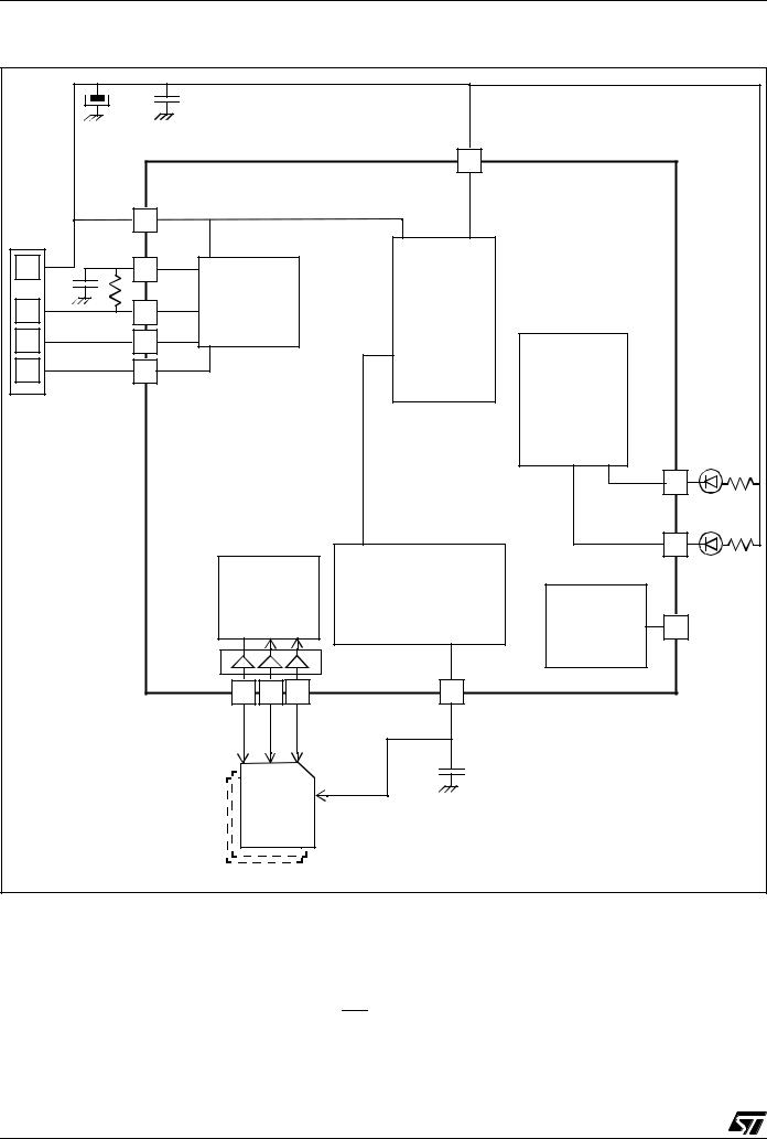
ST7265x
Figure 7. Multimedia Card Or Secure Digital Card Writer Application Example
|
μ |
F |
100nF |
|
|
|
|
|
|
4.7 |
|
|
|
|
|
|
|
|
|
|
|
|
|
VDD |
|
|
|
USBVDD |
|
|
|
|
|
|
|
|
=4.0-5.5V |
|
|
USBVDD |
|
|
|
|
USB Port |
|
|
|
|
|
|
|
|
5V |
1.5KΩ USB |
|
|
|
|
|
||
|
VCC |
|
|
|
|
|
||
|
|
|
|
|
|
|
||
|
100nF |
|
|
USB |
|
POWER |
|
|
DP |
|
|
DP |
|
|
|
||
|
|
MANAGEMENT |
|
|
||||
|
|
|
|
|
||||
|
|
|
|
|
|
|
||
DM |
|
|
DM |
|
|
(2) |
|
|
|
|
|
|
|
|
|
||
GND |
|
USB |
|
|
|
|
|
|
|
|
GND |
|
|
I/O |
|
|
|
|
|
|
|
|
|
|
|
|
|
|
|
|
|
|
LOGIC |
|
|
|
|
|
|
|
|
|
|
LED1 |
|
|
|
|
|
|
|
|
LED2 |
|
|
|
|
DTC |
REGULATOR |
|
|
|
|
|
|
|
|
|
FLASH |
VPP |
12V for |
|
|
|
|
|
|
|
|
Flash prog. |
|
|
|
|
|
|
|
|
(connect to |
|
|
|
|
|
level translator |
VDDF |
|
GND if |
|
|
|
|
|
|
|
|
not used) |
|
|
|
|
PE7 PE6 PE5 |
|
|
|
|
|
|
|
|
CLK DAT CMD |
|
100nF |
|
|
|
|
|
|
VDD |
|
|
|
|
|
|
|
|
UP TO 5 |
|
|
|
|
|
|
|
|
MULTIMEDIA |
|
|
|
|
|
|
|
|
OR SD CARDS |
|
|
|
|
MultiMedia Card Pin |
CMD |
DAT |
CLK |
|
|
|
|
ST72F65 pin |
PE5 |
PE6 |
PE7 |
|
|
|
|
ST7 / DTC (1) |
DTC |
DTC |
DTC |
(1)This line shows if the ST72F65 pin is controlled by the ST7 core or by the DTC.
(2)As this is a single power supply application, the USBEN function in not needed. Thus PF4/USBEN pin can be
used as a normal I/O by configuring it as such by the option byte.
14/166
1
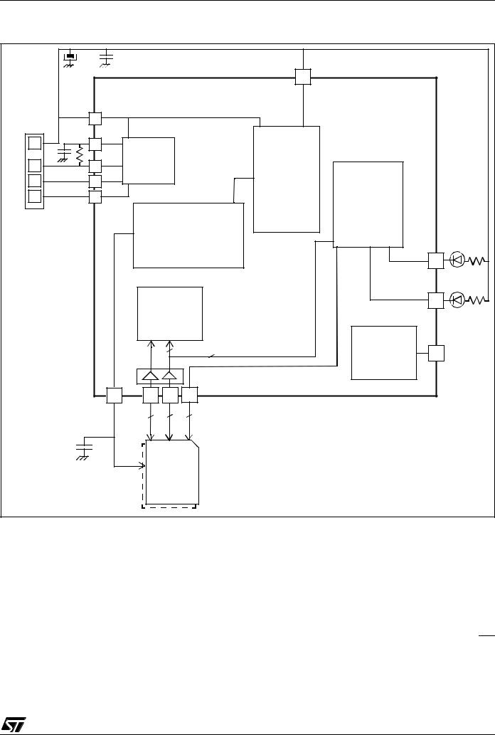
ST7265x
Figure 8. Smartmedia Card Writer Or Flash Drive Application Example
|
μ |
100nF |
|
|
|
|
|
|
|
4.7 F |
|
|
|
VDD |
|
|
|
|
|
|
|
|
|
|
|
|
|
USBVDD |
|
|
|
|
|
|
|
|
=4.0-5.5V |
|
USBVDD |
|
|
|
|
|
USB Port |
|
|
|
|
|
|
|
|
5V |
1.5KΩ USB |
|
|
|
|
|
|
|
|
VCC |
|
|
|
|
|
|
|
|
|
|
|
|
|
|
|
|
|
100nF |
|
USB |
|
|
|
|
|
DP |
|
DP |
|
|
POWER |
|
|
|
|
|
|
|
|
|
|||
|
|
|
|
|
|
|
|
|
DM |
|
DM |
|
|
|
MANAGEMENT |
|
|
GND |
|
USB |
|
|
|
(4) |
|
|
|
|
|
|
I/O |
|
|
||
|
|
GND |
|
|
|
|
|
|
|
|
|
|
|
|
LOGIC |
|
|
|
|
|
|
REGULATOR |
|
|
|
|
|
|
|
|
|
|
|
|
LED1 |
|
|
|
|
DTC |
|
|
|
LED2 |
|
|
|
|
5 |
1 |
FLASH |
VPP |
12V for |
|
|
|
level translator |
|
|
|
Flash prog. |
|
|
|
|
|
|
|
(connect to |
||
|
|
|
|
|
|
|
|
|
|
|
VDDF |
|
|
|
|
GND if |
|
|
|
|
|
|
PE |
|
|
not used) |
|
|
|
PB |
PA |
|
|
|
|
|
|
|
8 |
6 |
2 |
|
|
|
|
100nF |
|
|
|
|
|
|
|
|
|
|
I/O |
CTRL |
|
|
|
|
|
|
|
0~7 |
|
|
|
|
|
|
|
|
VDD |
|
|
|
|
|
|
|
|
UP TO 2 |
|
|
|
||
|
|
|
SMARTMEDIA |
|
|
|
||
|
|
|
|
CARDS |
|
|
|
|
Table 2. SmartMedia Interface Pin Assignment
SmartMedia Pin |
I/O0~7 |
CLE |
WE |
ALE |
RE |
R/B |
|
WP(2) |
CE1(2) |
CE2(2)(3) |
|
ST72F65 pin |
PB0-7 |
PA0 |
PA1 |
PA2 |
PA3 |
PA4 |
PA7 |
PE1 |
PE0 |
||
|
|
|
|
|
|
|
|
|
|
||
ST7 / DTC (1) |
DTC |
DTC |
DTC |
DTC |
DTC |
DTC |
ST7 |
ST7 |
ST7 |
||
(1): This line shows if the ST72F65 pin is controlled by the ST7 core or the DTC.
(2): These lines are not controlled by the DTC but by the user software running on the ST7 core. The ST72F65 pin choice is at customer discretion. The pins shown here are only shown as an example.
(3): When a single card is to be handled, PA7 is free for other functions. When 2 Smartmedia are to be handled, pins from both cards should be tied together (i.e. CLE1
with CLE2...) except for the CE pins. CE pin from card 1 should be connected to PA6 and CE pin from card 2 should be connect to PA7. Selection of the operating card is done by ST7 software.
(4) As this is a single power supply application, the USBEN function in not needed. Thus PF4/USBEN pin can be used as a normal I/O by configuring it as such by the option byte.
15/166
1
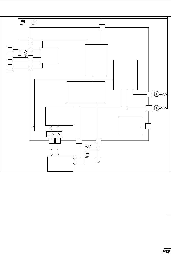
ST7265x
Figure 9. Compact Flash Card Writer Application Example
|
μ |
100nF |
|
|
|
|
|
|
4.7 F |
|
|
VDD |
|
|
|
|
|
|
|
|
|
|
|
|
USBVDD |
|
|
|
|
|
|
|
=4.0-5.5V |
|
USBVDD |
|
|
|
|
USB Port |
|
|
|
|
|
|
|
5V |
1.5KΩ USB |
|
|
|
|
|
|
|
VCC |
|
|
|
|
|
|
|
|
|
|
|
|
|
|
|
100nF |
|
USB |
|
POWER |
|
|
DP |
|
DP |
|
|
|
||
|
|
|
|
|
|||
|
|
|
MANAGEMENT |
|
|
||
|
|
|
|
|
|
|
|
DM |
|
DM |
|
|
(3) |
|
|
GND |
|
USB |
|
|
|
|
|
|
|
GND |
|
|
|
|
|
|
|
|
|
|
I/O |
|
|
|
|
|
|
|
LOGIC |
|
|
|
|
|
|
|
REGULATOR |
|
|
|
|
|
|
|
|
|
LED1 |
|
|
|
|
|
|
|
LED2 |
|
|
|
|
DTC |
|
|
|
|
|
|
1 |
|
FLASH |
VPP |
12V for |
|
|
|
|
Flash prog. |
|||
|
|
|
|
|
|||
|
|
|
5 |
|
|
|
(connect to |
|
|
|
level |
|
VDDF |
|
|
|
|
|
translator |
|
|
GND if |
|
|
|
|
PA |
|
PE |
|
not used) |
|
|
|
PB |
|
|
||
|
|
|
[2] |
|
|
||
|
|
|
|
|
4.7KΩ |
|
|
|
|
|
6 |
8 |
|
|
|
|
|
|
|
|
4.7µF |
|
|
|
|
|
|
CF |
100nF |
|
|
|
|
|
8-BIT MEMORY |
|
|
|
|
|
|
|
|
MODE |
|
|
|
Table 3. Compact Flash Card Writer Pin Assignment
|
|
|
|
|
|
|
|
|
|
|
|
|
|
|
|
|
|
|
|
|
|
CSEL, |
|
|
|
|
|
|
|
|
|
|
|
|
|
CD2, |
|
|
|
VS1, VS2, WAIT, |
|
|
|
|
|
|
|
|
|
|
|
|
|
|
|
|
|
|
|
|
|||||||||||||
Compact Flash |
|
|
|
IORD, |
|
|
|
|
|
|
|
|
|
|
|
|
|
|||||||||||||||||||
|
|
|
RESET, |
|
|
|
|
|
|
|
|
|
|
|
|
|
||||||||||||||||||||
D0-7 |
D8-15 |
|
|
|
|
|
, |
|
|
|
, |
|
IOWR |
, |
REG, |
|
A0-2 |
|
CE1 |
|
|
RE |
|
|
WE |
|
|
CD1 |
|
RDY/BSY, |
||||||
|
|
CS1 |
INPACK |
|||||||||||||||||||||||||||||||||
Card Pin |
|
|
|
|
BVD1, BVD2 |
|
CE2, VCC |
|
GND, |
|
|
|
|
|
|
|
|
|
|
|
|
|
WP |
|||||||||||||
|
|
|
|
|
|
|
A3-10 |
|
|
|
|
|
|
|
|
|
|
|
|
|
||||||||||||||||
|
|
|
|
|
|
|
|
|
|
|
|
|
|
|
|
|
|
|
|
|
|
|
|
|
|
|
|
|
|
|
|
|
|
|
|
|
|
|
|
|
|
|
|
|
|
|
|
|
|
|
|
|
|
|
|
|
|
|
|
|
|
|
|
|
|
|
|
|
|
|
|||
|
|
|
|
|
|
|
|
|
|
|
|
|
|
|
|
|
|
|
|
|
|
|
|
PE2 |
|
|
|
|
|
|
|
PA6 |
|
|||
ST72F65 pin |
PB0-7 |
NC |
|
|
|
|
|
|
NC |
|
|
VDDF |
|
VSSF |
PA0-2 |
+pull-up |
PA3 |
PA5 |
+pull-up |
NC |
||||||||||||||||
|
|
|
|
|
|
|
|
|
|
|
|
|
|
|
|
|
|
|
|
|
|
|
|
4.7kΩ |
|
|
|
|
|
|
100kΩ |
|
||||
|
|
|
|
|
|
|
|
|
|
|
|
|
|
|
|
|
|
|||||||||||||||||||
ST7 / DTC (1) |
DTC |
- |
- |
|
|
|
|
|
Power |
Power |
DTC |
ST7 |
DTC |
DTC |
|
ST7 |
- |
|||||||||||||||||||
(1)This line shows if the ST72F65 pin is controlled by the ST7 core or by the DTC.
(2)These lines are not controlled by the DTC but by the user software running on the ST7 core. The choice of ST72F65 pin is at the customer’s discretion. The pins shown here are given only as an example.
(3) As this is a single power supply application, the USBEN function in not needed. Thus PF4/USBEN pin can be used as a normal I/O by configuring it as such by the option byte.
16/166
1
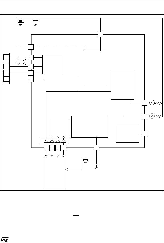
ST7265x
Figure 10. Sony Memory Stick Writer Application Example
|
μ |
F |
100nF |
|
|
|
|
|
|
|
4.7 |
|
|
|
|
|
|
|
|
|
|
|
|
|
|
|
VDD |
|
|
|
USBVDD |
|
|
|
|
|
|
|
|
|
=4.0-5.5V |
|
|
USBVDD |
|
|
|
|
|
USB Port |
|
|
|
|
|
|
|
|
|
5V |
1.5KΩ USB |
|
|
|
|
|
|
||
|
VCC |
|
|
|
|
|
|
||
|
|
|
|
|
|
|
|
||
|
100nF |
|
|
|
USB |
|
POWER |
|
|
DP |
|
|
DP |
|
|
|
|
||
|
|
|
MANAGEMENT |
|
|
||||
|
|
|
|
|
|
||||
|
|
|
|
|
|
|
|
||
DM |
|
|
DM |
|
|
|
(2) |
|
|
|
|
|
|
|
|
|
|
||
GND |
|
USB |
|
|
|
|
|
|
|
|
|
GND |
|
|
|
I/O |
|
|
|
|
|
|
|
|
|
|
|
|
|
|
|
|
|
|
|
|
LOGIC |
|
|
|
|
|
|
|
|
|
|
|
LED1 |
|
|
|
|
|
|
|
|
|
LED2 |
|
|
|
|
|
DTC |
REGULATOR |
|
|
|
|
|
|
|
|
|
|
FLASH |
VPP |
12V for |
|
|
|
|
|
|
|
|
|
Flash prog. |
|
|
|
|
|
|
|
|
|
(connect to |
|
|
|
|
|
|
level translator |
VDDF |
|
GND if |
|
|
|
|
|
|
|
|
|
not used) |
|
|
|
|
PC0 |
PC3 PC1 PC2 |
|
|
|
|
|
|
|
|
CD |
CLK BS DAT |
|
4.7µF |
|
|
|
|
|
|
|
|
|
|
|
|
|
|
|
|
|
|
|
100nF |
|
|
|
|
|
|
|
VDD |
|
|
|
|
|
|
|
|
|
SONY |
|
|
|
|
|
|
|
|
MEMORY STICK |
|
|
|
|
|
MultiMedia Card Pin |
CMD |
DAT |
CLK |
|
|
|
|
ST72F65 pin |
PE5 |
PE6 |
PE7 |
|
|
|
|
ST7 / DTC (1) |
DTC |
DTC |
DTC |
(1)This line shows if the ST72F65 pin is controlled by the ST7 core or by the DTC.
(2)As this is a single power supply application, the USBEN function in not needed. Thus PF4/USBEN pin can be
used as a normal I/O by configuring it as such by the option byte.
17/166
1
ST7265x
3 REGISTER & MEMORY MAP
As shown in Figure 11, the MCU is capable of addressing 64 Kbytes of memories and I/O registers.
The available memory locations consist of 80 bytes of register locations, up to 5 Kbytes of RAM and up to 32 Kbytes of user program memory. The RAM space includes up to 256 bytes for the stack from 0100h to 01FFh.
Figure 11. Memory Map
The highest address bytes contain the user reset and interrupt vectors.
IMPORTANT: Memory locations noted “Reserved” must never be accessed. Accessing a reserved area can have unpredictable effects on the device.
|
|
|
|
|
|
|
|
|
|
|
|
|
|
|
|
|
|
|
|
|
|
|
|
|
|
|
|
|
|
|
|
|
|
|
|
|
|
|
|
|
|
0050h |
|
||||||
0000h |
|
|
|
|
|
|
|
|
|
|
|
|
|
|
|
|
|
|
|
|
|
|
Short Addressing |
|
|
HW Registers |
|||||||||||||||||||||||
|
|
|
|
|
|
|
|
|
|
00FFh |
RAM (176 Bytes) |
|||||||||||||
|
|
|
(see Table 4) |
|
|
|
|
|
|
|
|
|
|
|||||||||||
|
|
|
|
|
|
|
|
|
|
|
|
|
|
|
|
|
|
|
|
|
|
|
||
004Fh |
|
|
|
|
|
|
|
|
|
|
|
|
|
|
|
0100h |
Stack (256 Bytes) |
|||||||
|
|
|
|
|
|
|
|
|
|
|
|
|
|
|
|
|
|
|
|
|
|
|||
0050h |
|
|
512 Bytes RAM* |
|
|
|
|
|
|
|
|
|
01FFh |
|||||||||||
|
|
|
|
|
|
|
|
|
|
|
|
|||||||||||||
|
|
|
|
|
|
|
|
|
|
|
|
|
|
|||||||||||
|
|
|
|
|
|
|
|
|
|
|
|
|
||||||||||||
|
|
|
|
|
|
|
|
|
|
|
|
|
|
|
|
|
|
|
|
|
|
|
||
144Fh |
|
5 KBytes RAM* |
|
|
|
|
|
|
|
|
|
|
0200h |
16-bit Addressing RAM |
||||||||||
|
|
|
|
|
|
|
|
|
|
|
|
|
|
|
|
|
|
|||||||
|
|
|
|
|
|
|
|
|
|
|
|
|
|
|
|
|
|
|
|
|
|
|||
1450h |
|
DTC RAM (Write protected) |
|
|
|
|
|
|
|
|
|
|
|
|
|
|
|
|
||||||
|
|
|
|
|
|
|
|
|
|
|
|
|
|
|
|
|
(80 Bytes) |
|||||||
154Fh |
|
|
256 Bytes |
|
|
|
|
|
|
|
|
|
|
024Fh |
|
|||||||||
|
|
|
USB Data Buffer** |
|
|
|
|
|
|
|
|
|
|
|||||||||||
|
|
|
|
|
|
|
|
|
|
|
|
|
|
|
|
|
|
|
|
|||||
|
|
|
|
|
|
|
|
|
|
|
|
|
|
|
|
|
|
|
|
|||||
1A4Fh |
|
|
1280 Bytes |
|
|
|
|
|
|
|
|
|
|
|
|
|
|
|
|
|
||||
|
|
|
|
|
|
|
|
|
|
|
|
|
|
|
|
|
|
|||||||
|
|
|
|
|
|
|
|
|
|
|
|
|
|
|
|
|
|
|
|
|
|
|
||
7FFFh |
|
Reserved |
|
|
|
|
|
|
|
|
|
0050h |
Short Addressing |
|||||||||||
|
|
|
|
|
|
|
|
|
|
|
|
|
|
|
|
|
||||||||
|
|
|
|
|
|
|
|
|
|
|
|
|
|
|
00FFh |
RAM (176 Bytes) |
||||||||
|
|
|
|
|
|
|
|
|
|
|
|
|
|
|
||||||||||
8000h |
|
Program Memory* |
|
|
|
|
|
|
|
|
|
|
||||||||||||
|
|
|
|
|
|
|
|
|
|
|
|
|
|
|
|
|
|
|
|
|||||
|
|
|
|
|
|
|
|
|
|
|
|
0100h |
Stack (256 Bytes) |
|||||||||||
|
|
|
32 Kbytes |
|
|
|
|
|
|
|
|
|
01FFh |
|||||||||||
|
|
|
|
|
|
|
|
|
|
|
|
|
||||||||||||
|
|
|
|
|
|
|
|
|
|
|
|
|
||||||||||||
|
|
|
|
|
|
|
|
|
|
|
|
|
|
|
|
|
|
|
|
|
|
|
|
|
C000h |
|
|
|
|
|
|
|
|
|
|
|
|
|
|
|
0200h |
|
|
|
|||||
|
|
|
|
|
|
|||||||||||||||||||
|
|
|
|
|
|
|
|
|
|
|
|
|
|
|
|
|
|
|
|
|
|
|
||
|
|
|
|
|
|
|
|
|
|
|
|
|
|
|
|
|
|
|
|
|
|
|
|
16-bit Addressing RAM |
|
|
|
16 Kbytes |
|
|
|
|
|
|
|
|
|
|
|
|
|
|
|
|
(4688 Bytes) |
||||
|
|
|
|
|
|
|
|
|
|
|
|
|
|
|
|
|
144Fh |
|
||||||
|
|
|
|
|
|
|
|
|
|
|
|
|
|
|
|
|
|
|
|
|
|
|
|
|
FFDFh
FFE0h
Interrupt & Reset Vectors
(see Table 10)
FFFFh
*Program memory and RAM sizes are product dependent (see Table –)
**The ST7 core is not able to read or write in the USB data buffer if the ST7265x is running at 6Mz in standalone mode.
18/166
1

|
|
|
|
|
ST7265x |
|
Table 4. Hardware Register Memory Map |
|
|
|
|||
|
|
|
|
|
|
|
Address |
Block |
Register Label |
Register name |
Reset Status |
Remarks |
|
|
|
|
|
|
|
|
0000h |
|
PADR |
Port A Data Register |
00h |
R/W |
|
0001h |
|
PADDR |
Port A Data Direction Register |
00h |
R/W |
|
0002h |
|
PAOR |
Port A Option Register |
00h |
R/W |
|
|
|
|
|
|
|
|
0003h |
|
PBDR |
Port B Data Register |
00h |
R/W |
|
0004h |
|
PBDDR |
Port B Data Direction Register |
00h |
R/W |
|
|
|
|
|
|
|
|
0005h |
|
|
Reserved Area (1 byte) |
|
|
|
|
|
|
|
|
|
|
0006h |
|
PCDR |
Port C Data Register |
00h |
R/W |
|
0007h |
|
PCDDR |
Port C Data Direction Register |
00h |
R/W |
|
0008h |
|
PCOR |
Port C Option Register |
00h |
R/W |
|
|
|
|
|
|
|
|
0009h |
|
PDDR |
Port D Data Register |
00h |
R/W |
|
000Ah |
|
PDDDR |
Port D Data Direction Register |
00h |
R/W |
|
000Bh |
|
PDOR |
Port D Option Register |
00h |
R/W |
|
|
|
|
|
|
|
|
000Ch |
|
PEDR |
Port E Data Register |
00h |
R/W |
|
000Dh |
|
PEDDR |
Port E Data Direction Register |
00h |
R/W |
|
000Eh |
|
PEOR |
Port E Option Register |
00h |
R/W |
|
|
|
|
|
|
|
|
000Fh |
|
PFDR |
Port F Data Register |
00h |
R/W |
|
0010h |
|
PFDDR |
Port F Data Direction Register |
00h |
R/W |
|
|
|
|
|
|
|
|
0011h |
|
|
Reserved Area (1 byte) |
|
|
|
|
|
|
|
|
|
|
0012h |
ADC1 |
ADCDR |
ADC Data Register |
00h |
Read only |
|
0013h |
ADCCSR |
ADC Control Status Register |
00h |
R/W |
|
|
|
|
|||||
|
|
|
|
|
|
|
0014h |
WDG |
WDGCR |
Watchdog Control Register |
7Fh |
R/W |
|
|
|
|
|
|
|
|
0015h |
|
|
|
|
|
|
to |
|
|
Reserved Area (3 bytes) |
|
|
|
0017h |
|
|
|
|
|
|
|
|
|
|
|
|
|
0018h |
DSM |
PCR |
Power Control Register |
00h |
R/W |
|
|
|
|
|
|
|
|
0019h |
|
SPIDR |
SPI Data I/O Register |
xxh |
R/W |
|
001Ah |
SPI |
SPICR |
SPI Control Register |
0xh |
R/W |
|
001Bh |
|
SPICSR |
SPI Control/Status Register |
00h |
R/W |
|
|
|
|
|
|
|
|
001Ch |
|
DTCCR |
DTC Control Register |
00h |
R/W |
|
001Dh |
DTC |
DTCSR |
DTC Status Register |
00h |
R/W |
|
001Eh |
Reserved |
|
|
|
|
|
|
|
|
|
|
||
001Fh |
|
DTCPR |
DTC Pointer Register |
00h |
R/W |
|
|
|
|
|
|
|
|
19/166
1

ST7265x
Address |
Block |
Register Label |
Register name |
Reset Status |
Remarks |
|
|
|
|
|
|
|
|
0020h |
|
TCR1 |
Timer Control Register 1 |
00h |
R/W |
|
0021h |
|
TCR2 |
Timer Control Register 2 |
00h |
R/W |
|
0022h |
|
TSR |
Timer Status Register |
00h |
Read Only |
|
0023h |
|
CHR |
Timer Counter High Register |
FFh |
Read Only |
|
0024h |
|
CLR |
Timer Counter Low Register |
FCh |
Read Only |
|
0025h |
TIM |
ACHR |
Timer Alternate Counter High Register |
FFh |
Read Only |
|
0026h |
|
ACLR |
Timer Alternate Counter Low Register |
FCh |
Read Only |
|
0027h |
|
OC1HR |
Timer Output Compare 1 High Register |
80h |
R/W |
|
0028h |
|
OC1LR |
Timer Output Compare 1 Low Register |
00h |
R/W |
|
0029h |
|
OC2HR |
Timer Output Compare 2 High Register |
80h |
R/W |
|
002Ah |
|
OC2LR |
Timer Output Compare 2 Low Register |
00h |
R/W |
|
|
|
|
|
|
|
|
002Bh |
Flash |
|
Flash Control Status Register |
00h |
R/W |
|
|
|
|
|
|
|
|
002Ch |
|
ITSPR0 |
Interrupt Software Priority Register 0 |
FFh |
R/W |
|
002Dh |
ITC |
ITSPR1 |
Interrupt Software Priority Register 1 |
FFh |
R/W |
|
002Eh |
ITSPR2 |
Interrupt Software Priority Register 2 |
FFh |
R/W |
|
|
|
|
|||||
002Fh |
|
ITSPR3 |
Interrupt Software Priority Register 3 |
FFh |
R/W |
|
|
|
|
|
|
|
|
0030h |
|
USBISTR |
USB Interrupt Status Register |
00h |
R/W |
|
0031h |
|
USBIMR |
USB Interrupt Mask Register |
00h |
R/W |
|
0032h |
|
USBCTLR |
USB Control Register |
06h |
R/W |
|
0033h |
|
DADDR |
Device Address Register |
00h |
R/W |
|
0034h |
|
USBSR |
USB Status Register |
00h |
R/W |
|
0035h |
|
EP0R |
Endpoint 0 Register |
00h |
R/W |
|
0036h |
|
CNT0RXR |
EP 0 Reception Counter Register |
00h |
R/W |
|
0037h |
USB |
CNT0TXR |
EP 0 Transmission Counter Register |
00h |
R/W |
|
0038h |
EP1RXR |
Endpoint 1 Register |
00h |
R/W |
|
|
|
|
|||||
0039h |
|
CNT1RXR |
EP 1 Reception Counter Register |
00h |
R/W |
|
003Ah |
|
EP1TXR |
Endpoint 1 Register |
00h |
R/W |
|
003Bh |
|
CNT1TXR |
EP 1 Transmission Counter Register |
00h |
R/W |
|
003Ch |
|
EP2RXR |
Endpoint 2 Register |
00h |
R/W |
|
003Dh |
|
CNT2RXR |
EP 2 Reception Counter Register |
00h |
R/W |
|
003Eh |
|
EP2TXR |
Endpoint 2 Register |
00h |
R/W |
|
003Fh |
|
CNT2TXR |
EP 2 Transmission Counter Register |
00h |
R/W |
|
|
|
|
|
|
|
|
0040h |
|
I2CCR |
I2C Control Register |
00h |
R/W |
|
0041h |
|
I2CSR1 |
I2C Status Register 1 |
00h |
Read only |
|
0042h |
|
I2CSR2 |
I2C Status Register 2 |
00h |
Read only |
|
0043h |
I2C 1 |
I2CCCR |
I2C Clock Control Register |
00h |
R/W |
|
0044h |
|
Not used |
|
|
|
|
0045h |
|
Not used |
|
|
|
|
0046h |
|
I2CDR |
I2C Data Register |
00h |
R/W |
|
0047h |
USB |
BUFCSR |
Buffer Control/Status Register |
00h |
R/W |
|
|
|
|
|
|
|
|
0048h |
|
|
Reserved Area (1 Byte) |
|
|
|
|
|
|
|
|
|
|
0049h |
|
MISCR1 |
Miscellaneous Register 1 |
00h |
R/W |
|
|
|
|
|
|
|
|
004Ah |
|
MISCR2 |
Miscellaneous Register 2 |
00h |
R/W |
|
|
|
|
|
|
|
|
004Bh |
|
|
Reserved Area (1 Byte) |
|
|
|
|
|
|
|
|
|
|
20/166 |
|
|
|
|
|
|
|
|
|
|
|
|
|
1
|
|
|
|
|
ST7265x |
|
|
|
|
|
|
|
|
Address |
Block |
Register Label |
Register name |
Reset Status |
Remarks |
|
|
|
|
|
|
|
|
004Ch |
|
MISCR3 |
Miscellaneous Register 3 |
00h |
R/W |
|
|
|
|
|
|
|
|
004Dh |
|
PWM0 |
|
80h |
R/W |
|
004Eh |
PWM1 |
BRM10 |
10-bit PWM/BRM registers |
00h |
R/W |
|
004Fh |
|
PWM1 |
|
80h |
R/W |
|
|
|
|
|
|
|
|
Note 1. If the peripheral is present on the device (see Device Summary on page 1)
21/166
1
ST7265x
4 FLASH PROGRAM MEMORY
4.1 Introduction
The ST7 dual voltage High Density Flash (HDFlash) is a non-volatile memory that can be electrically erased as a single block or by individual sectors and programmed on a Byte-by-Byte basis using an external VPP supply.
The HDFlash devices can be programmed and erased off-board (plugged in a programming tool) or on-board using ICP (In-Circuit Programming) or IAP (In-Application Programming).
The array matrix organisation allows each sector to be erased and reprogrammed without affecting other sectors.
4.2 Main Features
■Three Flash programming modes:
–Insertion in a programming tool. In this mode, all sectors including option bytes can be programmed or erased.
–ICP (In-Circuit Programming). In this mode, all sectors including option bytes can be programmed or erased without removing the device from the application board.
–IAP (In-Application Programming) In this mode, all sectors except Sector 0, can be programmed or erased without removing the device from the application board and while the application is running.
■ICT (In-Circuit Testing) for downloading and executing user application test patterns in RAM
■Read-out protection against piracy
■Register Access Security System (RASS) to prevent accidental programming or erasing
Figure 12. Memory Map and Sector Address
4.3 Structure
The Flash memory is organised in sectors and can be used for both code and data storage.
Depending on the overall Flash memory size in the microcontroller device, there are up to three user sectors (see Table 5). Each of these sectors can be erased independently to avoid unnecessary erasing of the whole Flash memory when only a partial erasing is required.
The first two sectors have a fixed size of 4 Kbytes (see Figure 12). They are mapped in the upper part of the ST7 addressing space so the reset and interrupt vectors are located in Sector 0 (F000hFFFFh).
Table 5. Sectors available in Flash devices
Flash Memory Size |
Available Sectors |
|
(bytes) |
||
|
||
|
|
|
4K |
Sector 0 |
|
|
|
|
8K |
Sectors 0,1 |
|
|
|
|
> 8K |
Sectors 0,1, 2 |
|
|
|
4.4 Program Memory Read-out Protection
The read-out protection is enabled through an option bit.
When this option is selected, the programs and data stored in the program memory (Flash or ROM) are protected against read-out piracy (including a re-write protection). In Flash devices, when this protection is removed by reprogramming the Option Byte, the entire program memory is first automatically erased and the device can be reprogrammed.
Refer to the Option Byte description for more details.
4K |
8K |
10K |
16K |
24K |
32K |
48K |
60K |
|
|
DV FLASH |
|||||||||||||||
|
|
||||||||||||||||||||||||
|
|
|
|
|
|
|
|
|
|
|
|
|
|
|
|
|
|
|
|
|
|
|
|
|
MEMORY SIZE |
1000h
3FFFh
7FFFh
9FFFh
 SECTOR 2
BFFFh
D7FFh |
|
|
|
|
8 Kbytes 16 Kbytes 24 Kbytes 40 Kbytes |
52 Kbytes |
|||
DFFFh |
|
|
|
2 Kbytes |
|||||
|
|
|
|
|
|
|
|
|
|
EFFFh |
|
|
|
|
4 Kbytes |
|
|
|
SECTOR 1 |
|
|
|
|
|
|
|
|||
|
|
|
|
|
|
|
|
|
|
FFFFh |
|
|
|
|
4 Kbytes |
|
|
|
SECTOR 0 |
|
|
|
|
|
|
|
|||
22/166
1
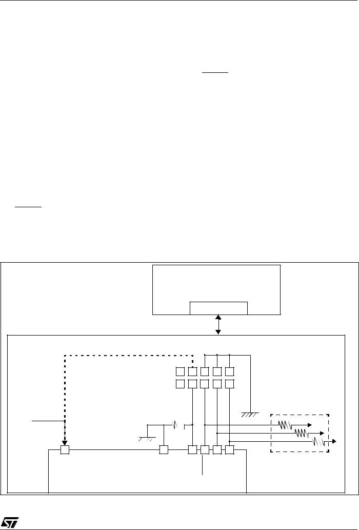
ST7265x
FLASH PROGRAM MEMORY (Cont’d)
4.5 ICP (In-Circuit Programming)
To perform ICP the microcontroller must be switched to ICC (In-Circuit Communication) mode by an external controller or programming tool.
Depending on the ICP code downloaded in RAM, Flash memory programming can be fully customized (number of bytes to program, program locations, or selection serial communication interface for downloading).
When using an STMicroelectronics or third-party programming tool that supports ICP and the specific microcontroller device, the user needs only to implement the ICP hardware interface on the application board (see Figure 13). For more details on the pin locations, refer to the device pinout description.
ICP needs six pins to be connected to the programming tool. These pins are:
–RESET: device reset
–VSS: device power supply ground
–ICCCLK: ICC output serial clock pin
–ICCDATA: ICC input serial data pin
Figure 13. Typical ICP Interface
–ICCSEL/VPP: programming voltage
–VDD: application board power supply
CAUTIONS:
1.If RESET, ICCCLK or ICCDATA pins are used for other purposes in the application, a serial resistor has to be implemented to avoid a conflict in case one of the other devices forces the signal level. If these pins are used as outputs in the application, the serial resistors are not necessary. As soon as the external controller is plugged to the board, even if an ICC session is not in progress, the ICCCLK and ICCDATA pins are not available for the application.
2.The use of Pin 7 of the ICC connector depends on the Programming Tool architecture. Please refer to the documentation of the tool. This pin must be connected when using ST Programming Tools (it is used to monitor the application power supply).
Note: To develop a custom programming tool, refer to the ST7 Flash Programming and ICC Reference Manual which gives full details on the ICC protocol hardware and software.
|
|
PROGRAMMING TOOL |
|
|||
|
|
ICC CONNECTOR |
|
|||
|
|
|
|
|
ICC Cable |
|
OPTIONAL |
ICC CONNECTOR |
|
||||
(SEE CAUTION 2) |
HE10 CONNECTOR TYPE |
|
||||
|
9 |
7 |
5 |
3 |
1 |
APPLICATION BOARD |
|
|
|||||
|
10 |
8 |
6 |
4 |
2 |
|
|
10kΩ |
|
|
|
|
>4.7kΩ |
APPLICATION |
|
|
|
|
|
|
POWER SUPPLY |
|
|
|
|
|
|
VDD |
|
ICCSEL/VPP |
RESET |
ICCCLK |
ICCDATA |
OPTIONAL (SEE CAUTION 1) |
ST7 |
|
|||||
VSS |
|
|||||
|
|
|
|
|
|
23/166 |
|
|
|
|
|
|
1 |

ST7265x
FLASH PROGRAM MEMORY (Cont’d)
4.6 IAP (In-Application Programming)
This mode uses a BootLoader program previously stored in Sector 0 by the user (in ICP mode or by plugging the device in a programming tool).
This mode is fully controlled by user software. This allows it to be adapted to the user application, (us- er-defined strategy for entering programming mode, choice of communications protocol used to fetch the data to be stored, etc.). For example, it is possible to download code from the SPI, SCI, USB or CAN interface and program it in the Flash. IAP mode can be used to program any of the Flash sectors except Sector 0, which is write/erase protected to allow recovery in case errors occur during the programming operation.
4.7 Related Documentation
For details on Flash programming and ICC protocol, refer to the ST7 Flash Programming Reference Manual and to the ST7 ICC Protocol Reference Manual.
Table 6. FLASH Register Map and Reset Values
4.8 Register Description
FLASH CONTROL/STATUS REGISTER (FCSR)
Read/Write
Reset Value: 0000 0000 (00h)
7 |
|
|
|
|
|
|
0 |
|
|
|
|
|
|
|
|
0 |
0 |
0 |
0 |
0 |
0 |
0 |
0 |
|
|
|
|
|
|
|
|
This register is reserved for use by Programming Tool software. It controls the Flash programming and erasing operations.
Address |
Register |
7 |
6 |
5 |
4 |
3 |
2 |
1 |
0 |
|
(Hex.) |
Label |
|||||||||
|
|
|
|
|
|
|
|
|||
|
|
|
|
|
|
|
|
|
|
|
002Bh |
FCSR |
|
|
|
|
|
|
|
|
|
Reset Value |
0 |
0 |
0 |
0 |
0 |
0 |
0 |
0 |
||
|
||||||||||
|
|
|
|
|
|
|
|
|
|
24/166
1

ST7265x
5 CENTRAL PROCESSING UNIT
5.1 INTRODUCTION
This CPU has a full 8-bit architecture and contains six internal registers allowing efficient 8-bit data manipulation.
5.2 MAIN FEATURES
■Enable executing 63 basic instructions
■Fast 8-bit by 8-bit multiply
■17 main addressing modes (with indirect addressing mode)
■Two 8-bit index registers
■16-bit stack pointer
■Low power HALT and WAIT modes
■Priority maskable hardware interrupts
■Non-maskable software/hardware interrupts
5.3 CPU REGISTERS
The 6 CPU registers shown in Figure 14 are not present in the memory mapping and are accessed by specific instructions.
Accumulator (A)
The Accumulator is an 8-bit general purpose register used to hold operands and the results of the arithmetic and logic calculations and to manipulate data.
Index Registers (X and Y)
These 8-bit registers are used to create effective addresses or as temporary storage areas for data manipulation. (The Cross-Assembler generates a precede instruction (PRE) to indicate that the following instruction refers to the Y register.)
The Y register is not affected by the interrupt automatic procedures.
Program Counter (PC)
The program counter is a 16-bit register containing the address of the next instruction to be executed by the CPU. It is made of two 8-bit registers PCL (Program Counter Low which is the LSB) and PCH (Program Counter High which is the MSB).
Figure 14. CPU Registers
|
|
|
|
|
|
|
|
|
|
7 |
|
|
|
|
|
|
|
0 |
|
|
|
|
||
|
|
|
|
|
|
|
|
|
|
|
|
|
|
|
|
|
|
|
|
|
|
|
|
ACCUMULATOR |
|
|
|
|
|
|
|
|
|
|
|
|
RESET VALUE = XXh |
|
|
|
|
|
|||||||
|
|
|
|
|
|
|
|
|
|
7 |
|
|
|
|
|
|
|
0 |
|
|
|
|
||
|
|
|
|
|
|
|
|
|
|
|
|
|
|
|
|
|
|
|
|
|
|
|
|
X INDEX REGISTER |
|
|
|
|
|
|
|
|
|
|
|
|
|
|
|
|
|
|
|
|
|
|
|
|
|
|
|
|
|
|
|
|
|
|
|
|
|
|
|
|
|
|
|
|
|
|
|
|
|
|
|
|
|
|
|
|
|
|
|
|
RESET VALUE = XXh |
|
|
|
|
|
|||||||||
|
|
|
|
|
|
|
|
|
|
7 |
|
|
|
|
|
|
|
0 |
|
|
|
|
||
|
|
|
|
|
|
|
|
|
|
|
|
|
|
|
|
|
|
|
|
|
|
|
|
Y INDEX REGISTER |
|
|
|
|
|
|
|
|
|
|
|
|
|
|
|
|
|
|
|
|
|
|
|
|
|
|
|
|
|
|
|
|
|
|
|
|
|
|
|
|
|
|
|
|
|
|
|
|
||
|
|
|
|
|
|
|
|
|
|
RESET VALUE = XXh |
|
|
|
|
|
|||||||||
|
|
|
|
|
PCH |
8 |
|
7 |
|
|
PCL |
|
0 |
|
|
|
PROGRAM COUNTER |
|||||||
|
15 |
|
|
|
|
|
|
|
|
|
||||||||||||||
|
|
|
|
|
|
|
|
|
||||||||||||||||
|
|
|
|
|
|
|
|
|
|
|
|
|
|
|
|
|
|
|
|
|
|
|
|
|
|
|
|
|
|
|
|
|
|
|
|
|
|
|
|
|
|
|
|
|
|
|
|
|
|
|
RESET VALUE = RESET VECTOR @ FFFEh-FFFFh |
|
||||||||||||||||||||||
|
|
|
|
|
|
|
|
|
|
7 |
|
|
|
|
|
|
|
0 |
|
|
|
|
||
|
|
|
|
|
|
|
|
|
|
|
|
|
|
|
|
|
|
|
|
|
|
|
|
|
|
|
|
|
|
|
|
|
|
|
|
|
1 |
1 |
I1 |
H |
I0 |
N |
|
Z |
C |
|
|
CONDITION CODE REGISTER |
|
|
|
|
|
|
|
|
|
|
|
|
|
|
|
|
|
|
|
|
|
|
|
|
|
|
|
|
|
|
RESET VALUE = 1 |
1 |
1 X |
1 X |
X |
X |
|
||||||||||||||
|
|
15 |
|
|
|
|
|
8 |
|
|
|
|
|
|
|
|
0 |
|
|
|
STACK POINTER |
|||
|
|
|
|
|
|
|
7 |
|
|
|
|
|
|
|
|
|
|
|||||||
|
|
|
|
|
|
|
|
|
|
|
|
|
|
|
|
|
|
|
|
|
|
|
|
|
RESET VALUE = STACK HIGHER ADDRESS |
|
|
|
|
|
|
||||||||||||||||||
X = Undefined Value
25/166
1

ST7265x
CENTRAL PROCESSING UNIT (Cont’d)
Condition Code Register (CC)
Read/Write
Reset Value: 111x1xxx
7 |
|
|
|
|
|
|
0 |
|
|
|
|
|
|
|
|
1 |
1 |
I1 |
H |
I0 |
N |
Z |
C |
|
|
|
|
|
|
|
|
The 8-bit Condition Code register contains the interrupt masks and four flags representative of the result of the instruction just executed. This register can also be handled by the PUSH and POP instructions.
These bits can be individually tested and/or controlled by specific instructions.
Arithmetic Management Bits
Bit 4 = H Half carry.
This bit is set by hardware when a carry occurs between bits 3 and 4 of the ALU during an ADD or ADC instructions. It is reset by hardware during the same instructions.
0:No half carry has occurred.
1:A half carry has occurred.
This bit is tested using the JRH or JRNH instruction. The H bit is useful in BCD arithmetic subroutines.
Bit 2 = N Negative.
This bit is set and cleared by hardware. It is representative of the result sign of the last arithmetic, logical or data manipulation. It’s a copy of the result 7th bit.
0:The result of the last operation is positive or null.
1:The result of the last operation is negative
(i.e. the most significant bit is a logic 1).
This bit is accessed by the JRMI and JRPL instructions.
26/166
Bit 1 = Z Zero.
This bit is set and cleared by hardware. This bit indicates that the result of the last arithmetic, logical or data manipulation is zero.
0:The result of the last operation is different from zero.
1:The result of the last operation is zero.
This bit is accessed by the JREQ and JRNE test instructions.
Bit 0 = C Carry/borrow.
This bit is set and cleared by hardware and software. It indicates an overflow or an underflow has occurred during the last arithmetic operation.
0:No overflow or underflow has occurred.
1:An overflow or underflow has occurred.
This bit is driven by the SCF and RCF instructions and tested by the JRC and JRNC instructions. It is also affected by the “bit test and branch”, shift and rotate instructions.
Interrupt Management Bits
Bit 5,3 = I1, I0 Interrupt
The combination of the I1 and I0 bits gives the current interrupt software priority.
Interrupt Software Priority |
I1 |
I0 |
|
|
|
|
|
Level 0 |
(main) |
1 |
0 |
|
|
|
|
Level 1 |
|
0 |
1 |
|
|
|
|
Level 2 |
|
0 |
0 |
|
|
|
|
Level 3 |
(= interrupt disable) |
1 |
1 |
|
|
|
|
These two bits are set/cleared by hardware when entering in interrupt. The loaded value is given by the corresponding bits in the interrupt software priority registers (IxSPR). They can be also set/ cleared by software with the RIM, SIM, IRET, HALT, WFI and PUSH/POP instructions.
See the interrupt management chapter for more details.
1
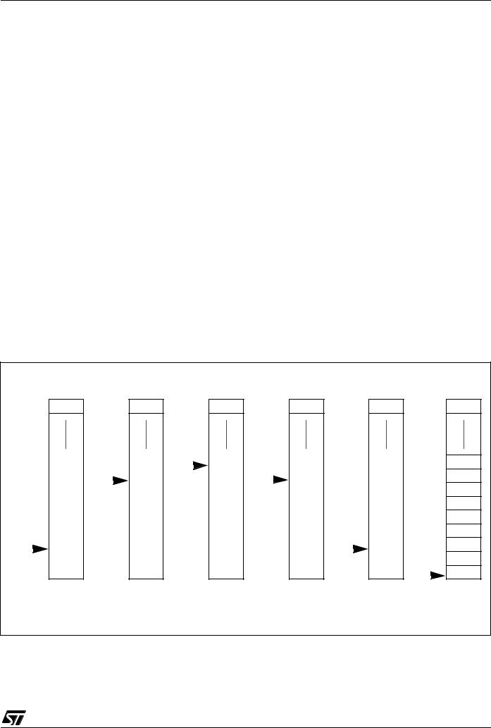
ST7265x
CENTRAL PROCESSING UNIT (Cont’d)
Stack Pointer (SP)
Read/Write
Reset Value: 01 FFh
15 |
|
|
|
|
|
|
8 |
|
|
|
|
|
|
|
|
0 |
0 |
0 |
0 |
0 |
0 |
0 |
1 |
|
|
|
|
|
|
|
|
7 |
|
|
|
|
|
|
0 |
|
|
|
|
|
|
|
|
SP7 |
SP6 |
SP5 |
SP4 |
SP3 |
SP2 |
SP1 |
SP0 |
|
|
|
|
|
|
|
|
The Stack Pointer is a 16-bit register which is always pointing to the next free location in the stack. It is then decremented after data has been pushed onto the stack and incremented before data is popped from the stack (see Figure 15).
Since the stack is 256 bytes deep, the 8 most significant bits are forced by hardware. Following an MCU Reset, or after a Reset Stack Pointer instruction (RSP), the Stack Pointer contains its reset value (the SP7 to SP0 bits are set) which is the stack higher address.
Figure 15. Stack Manipulation Example
The least significant byte of the Stack Pointer (called S) can be directly accessed by a LD instruction.
Note: When the lower limit is exceeded, the Stack Pointer wraps around to the stack upper limit, without indicating the stack overflow. The previously stored information is then overwritten and therefore lost. The stack also wraps in case of an underflow.
The stack is used to save the return address during a subroutine call and the CPU context during an interrupt. The user may also directly manipulate the stack by means of the PUSH and POP instructions. In the case of an interrupt, the PCL is stored at the first location pointed to by the SP. Then the other registers are stored in the next locations as shown in Figure 15.
–When an interrupt is received, the SP is decremented and the context is pushed on the stack.
–On return from interrupt, the SP is incremented and the context is popped from the stack.
A subroutine call occupies two locations and an interrupt five locations in the stack area.
CALL |
Interrupt |
PUSH Y |
POP Y |
IRET |
RET |
Subroutine |
Event |
|
|
|
or RSP |
@ 0100h
|
|
|
|
|
SP |
|
SP |
|
SP |
|
|
|
|
|
|
|
|
|
|||||||||
|
|
|
|
|
|
|
|
|
|
|
|
|
|
|
|
||||||||||||
|
|
|
|
|
|
|
|
|
|
|
|
|
|
|
|
|
|
|
|
||||||||
|
|
|
|
|
|
|
|
|
|
Y |
|
|
|
|
|
|
|
|
|
||||||||
|
|
|
|
|
|
|
|
|
|
|
|
|
|
|
|
|
|
|
|
|
|
|
|
|
|
|
|
|
|
|
|
|
|
|
|
|
CC |
|
|
|
|
CC |
|
|
|
|
CC |
|
|
|
|
|
|
|
|
|
|
|
|
|
|
|
|
|
A |
|
|
|
|
A |
|
|
|
|
A |
|
|
|
|
|
|
|
|
|
|
|
|
|
|
|
|
|
|
|
|
|
|
|
|
|
|
|
|
|
|
|
|
|
|
|
|
|
|
|
|
|
|
|
|
|
X |
|
|
|
|
X |
|
|
|
|
X |
|
|
|
|
|
|
|
|
|
|
|
|
|
|
|
|
|
|
|
|
|
|
|
|
|
|
|
|
|
|
|
|
|
|
|
|
SP |
|
|
|
|
|
PCH |
|
|
|
|
PCH |
|
|
|
|
PCH |
SP |
|
|
|
|
||||||
|
|
|
|
|
PCL |
|
|
|
|
PCL |
|
|
|
|
PCL |
|
|
|
|
||||||||
|
|
|
|
|
|
|
|
|
|
|
|
|
|
|
|
|
|
|
|
|
|
|
|
|
|||
|
|
|
|
PCH |
|
|
|
|
PCH |
|
|
|
|
PCH |
|
|
|
|
PCH |
|
|
|
|
PCH |
|
||
|
|
|
|
|
|
|
|
|
|
|
|
|
|
|
|
|
|
|
|
|
|
|
|
|
SP |
|
|
|
|
|
|
|
|
|
|
|
|
|
|
|
|
|
|
|
|
|
|
|
|
||||||
@ 01FFh PCL |
|
|
|
|
PCL |
|
|
|
|
PCL |
|
|
|
|
PCL |
|
|
|
|
PCL |
|
|
|||||
Stack Higher Address = 01FFh
Stack Lower Address = 0100h
27/166
1
ST7265x
6 SUPPLY, RESET AND CLOCK MANAGEMENT
6.1 CLOCK SYSTEM
6.1.1 General Description
The MCU accepts either a 12 MHz crystal or an external clock signal to drive the internal oscillator. The internal clock (fCPU) is derived from the internal oscillator frequency (fOSC), which is 12 Mhz in Stand-alone mode and 48Mhz in USB mode.
The internal clock (fCPU) is software selectable using the CP[1:0] and CPEN bits in the MISCR1 register.
In USBVDD power supply mode, the PLL is active, generating a 48MHz clock to the USB. In this mode, fCPU can be configured to be up to 8 MHz. In VDD mode the PLL and the USB clock are disabled, and the maximum frequency of fCPU is 6 MHz.
The internal clock signal (fCPU) is also routed to the on-chip peripherals. The CPU clock signal consists of a square wave with a duty cycle of 50%.
The internal oscillator is designed to operate with an AT-cut parallel resonant quartz in the frequency range specified for fosc. The circuit shown in Figure 17 is recommended when using a crystal, and Table 7 lists the recommended capacitance. The crystal and associated components should be mounted as close as possible to the input pins in order to minimize output distortion and start-up stabilisation time.
Table 7. Recommended |
Values |
for 12-MHz |
|||
Crystal Resonator |
|
|
|
||
|
|
|
|
|
|
RSMAX |
20 Ω |
|
25 Ω |
|
70 Ω |
COSCIN |
56pF |
|
47pF |
|
22pF |
COSCOUT |
56pF |
|
47pF |
|
22pF |
Note: RSMAX is the equivalent serial resistor of the crystal (see crystal specification).
6.1.2 External Clock
An external clock may be applied to the OSCIN input with the OSCOUT pin not connected, as shown on Figure 16. The tOXOV specifications does not apply when using an external clock input. The equivalent specification of the external clock
source should be used instead of tOXOV (see Section 6.5 CONTROL TIMING).
Figure 16. External Clock Source Connections
OSCIN OSCOUT
NC
EXTERNAL
CLOCK
Figure 17. Crystal Resonator
OSCIN OSCOUT
|
|
|
|
|
|
|
|
|
|
|
|
|
|
COSCIN |
|
|
|
|
|
|
|
|
|
|
COSCOUT |
||
|
|
|
|
|
|
|
|
|
|
||||
|
|
|
|
|
|
|
|
|
|
||||
|
|
|
|
|
|
|
|
|
|
||||
|
|
|
|
|
|
|
|
|
|
||||
|
|
|
|
|
|
|
|
|
|
|
|
|
|
|
|
|
|
|
|
|
|
|
|
|
|
|
|
|
|
|
|
|
|
|
|
|
|
|
|
|
|
28/166
1
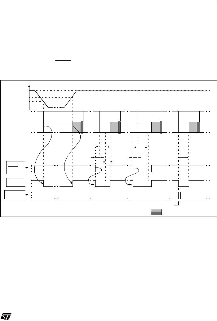
ST7265x
6.2 RESET SEQUENCE MANAGER (RSM)
6.2.1 Introduction
The reset sequence manager includes three RESET sources as shown in Figure 6.2.2:
■External RESET source pulse
■Internal LVD RESET (Low Voltage Detection)
■Internal WATCHDOG RESET
These sources act on the RESET pin and it is always kept low during the delay phase.
The RESET service routine vector is fixed at addresses FFFEh-FFFFh in the ST7 memory map.
The basic RESET sequence consists of 3 phases as shown in Figure 18:
■Active Phase depending on the RESET source
■Min 512 CPU clock cycle delay (see Figure 20 and Figure 21
■RESET vector fetch
Figure 18. RESET Sequences
VDD
VIT+(LVD)
VIT-(LVD)
LVD |
SHORT EXT. |
|
RESET |
RESET |
|
RUN |
RUN |
|
ACTIVE PHASE |
ACTIVE |
|
PHASE |
||
|
LONG EXT. |
|
WATCHDOG |
RESET |
|
RESET |
RUN |
RUN |
RUN |
ACTIVE |
|
ACTIVE |
PHASE |
|
PHASE |
tw(RSTL)out |
|
tw(RSTL)out |
|
|
th(RSTL)in |
|
th(RSTL)in |
|
tw(RSTL)out |
 DELAY
DELAY
EXTERNAL
RESET
SOURCE
RESET PIN 
WATCHDOG
RESET
WATCHDOG UNDERFLOW
INTERNAL RESET (min 512 TCPU)
VECTOR FETCH
29/166
1
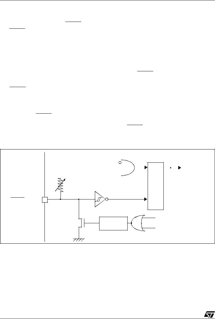
ST7265x
RESET SEQUENCE MANAGER (Cont’d)
6.2.2 Asynchronous External RESET pin
The RESET pin is both an input and an open-drain output with integrated RON weak pull-up resistor. This pull-up has no fixed value but varies in accordance with the input voltage. It can be pulled low by external circuitry to reset the device. See electrical characteristics section for more details.
A RESET signal originating from an external
source must have a duration of at least th(RSTL)in in order to be recognized. This detection is asynchro-
nous and therefore the MCU can enter reset state even in HALT mode.
The RESET pin is an asynchronous signal which plays a major role in EMS performance. In a noisy environment, it is recommended to follow the guidelines mentioned in the electrical characteristics section.
If the external RESET pulse is shorter than
tw(RSTL)out (see short ext. Reset in Figure 18), the signal on the RESET pin will be stretched. Other-
wise the delay will not be applied (see long ext. Reset in Figure 18).
Figure 19. Reset Block Diagram
Starting from the external RESET pulse recognition, the device RESET pin acts as an output that is pulled low during at least tw(RSTL)out.
6.2.3 Internal Low Voltage Detection RESET
Two different RESET sequences caused by the internal LVD circuitry can be distinguished:
■Power-On RESET
■Voltage Drop RESET
The device RESET pin acts as an output that is pulled low when VDD<VIT+ (rising edge) or VDD<VIT- (falling edge) as shown in Figure 18.
The LVD filters spikes on VDD shorter than tg(VDD) to avoid parasitic resets.
6.2.4 Internal Watchdog RESET
The RESET sequence generated by a internal Watchdog counter overflow is shown in Figure 18.
Starting from the Watchdog counter underflow, the device RESET pin acts as an output that is pulled low during at least tw(RSTL)out.
VDD |
|
|
|
|
|
|
|
|
|
INTERNAL |
|||
|
|
|
|
|
|
|
|
|
|||||
|
fCPU |
|
|
|
|
|
|||||||
|
|
|
|
|
|
|
|
|
|
RESET |
|||
|
|
|
|
||||||||||
|
|
|
|
RON |
|
|
COUNTER |
||||||
|
|
|
|
|
|
||||||||
|
|
|
|
||||||||||
|
|
|
|
|
|
|
|
|
|
||||
RESET 

WATCHDOG RESET
PULSE
GENERATOR
LVD RESET
30/166
1
 Loading...