


SGS Thomson Microelectronics M28F101-120N1, M28F101-100P1, M28F101-150P6, M28F101-150P1, M28F101-150K1 Datasheet
M28F101
1 Mb (128K x 8, Chip Erase) FLASH MEMORY
5V ±10% SUPPLY VOLTAGE
12V PROGRAMMING VOLTAGE FAST ACCESS TIME: 70ns
BYTE PROGRAMING TIME: 10μs typical ELECTRICAL CHIP ERASE in 1s RANGE LOW POWER CONSUMPTION
± Stand-by Current: 100μA max 10,000 ERASE/PROGRAM CYCLES
INTEGRATED ERASE/PROGRAM-STOP TIMER
OTP COMPATIBLE PACKAGES and PINOUTS ELECTRONIC SIGNATURE
±Manufacturer Code: 20h
±Device Code: 07h
DESCRIPTION
The M28F101 FLASH Memory is a non-volatile memory which may be erased electrically at the chip level and programmed byte-by-byte. It is organised as 128K bytes of 8 bits. It uses a command register architecture to select the operating modes and thus provides a simple microprocessor interface. The M28F101 FLASH Memory is suitable for applications where the memory has to be reprogrammed in the equipment. The access time of 70ns makes the device suitable for use in high speed microprocessor systems.
Table 1. Signal Names
A0-A16 |
Address Inputs |
DQ0-DQ7 |
Data Inputs / Outputs |
E |
Chip Enable |
G |
Output Enable |
W |
Write Enable |
VPP |
Program Supply |
VCC |
Supply Voltage |
VSS |
Ground |
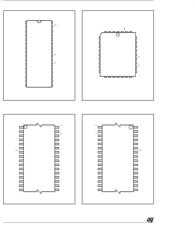
32
1 |
|
PDIP32 (P) |
PLCC32 (K) |
TSOP32 (N) 8 x 20 mm
Figure 1. Logic Diagram
VCC |
VPP |
17 |
8 |
A0-A16 |
DQ0-DQ7 |
W M28F101
E
G
VSS
AI00666B
April 1997 |
1/23 |
M28F101
Figure 2A. DIP Pin Connections
VPP |
1 |
|
32 |
VCC |
A16 |
2 |
|
31 |
W |
A15 |
3 |
|
30 |
NC |
A12 |
4 |
|
29 |
A14 |
A7 |
5 |
|
28 |
A13 |
A6 |
6 |
|
27 |
A8 |
A5 |
7 |
|
26 |
A9 |
A4 |
8 |
M28F101 |
25 |
A11 |
A3 |
9 |
|
24 |
G |
A2 |
10 |
|
23 |
A10 |
A1 |
11 |
|
22 |
E |
A0 |
12 |
|
21 |
DQ7 |
DQ0 |
13 |
|
20 |
DQ6 |
DQ1 |
14 |
|
19 |
DQ5 |
DQ2 |
15 |
|
18 |
DQ4 |
VSS |
16 |
|
17 |
DQ3 |
|
|
AI00667 |
|
|
Warning: NC = Not Connected.
Figure 2C. TSOP Pin Connections
A11 |
1 |
|
32 |
G |
A9 |
|
|
|
A10 |
A8 |
|
|
|
E |
A13 |
|
|
|
DQ7 |
A14 |
|
|
|
DQ6 |
NC |
|
|
|
DQ5 |
W |
|
|
|
DQ4 |
VCC |
8 |
M28F101 |
25 |
DQ3 |
VPP |
9 |
(Normal) |
24 |
VSS |
A16 |
|
|
|
DQ2 |
A15 |
|
|
|
DQ1 |
A12 |
|
|
|
DQ0 |
A7 |
|
|
|
A0 |
A6 |
|
|
|
A1 |
A5 |
|
|
|
A2 |
A4 |
16 |
|
17 |
A3 |
|
|
|
AI00669B |
|
Warning: NC = Not Connected.
Figure 2B. LCC Pin Connections
|
A12 |
A15 |
A16 |
PP |
CC |
W |
NC |
|
|
V |
V |
|
|||||
A7 |
|
|
|
1 |
32 |
|
|
A14 |
|
|
|
|
|
|
|
||
A6 |
|
|
|
|
|
|
|
A13 |
A5 |
|
|
|
|
|
|
|
A8 |
A4 |
|
|
|
|
|
|
|
A9 |
A3 |
9 |
|
M28F101 |
|
25 |
A11 |
||
A2 |
|
|
|
|
|
|
|
G |
A1 |
|
|
|
|
|
|
|
A10 |
A0 |
|
|
|
|
|
|
|
E |
DQ0 |
|
|
|
17 |
|
|
|
DQ7 |
|
DQ1 |
DQ2 |
|
DQ4 |
DQ5 |
DQ6 |
|
|
|
V |
DQ3 |
|
|||||
|
|
|
SS |
|
|
|
|
|
|
|
|
|
|
|
|
|
AI00668 |
Warning: NC = Not Connected.
Figure 2D. TSOP Reverse Pin Connections
G |
1 |
|
32 |
A11 |
A10 |
|
|
|
A9 |
E |
|
|
|
A8 |
DQ7 |
|
|
|
A13 |
DQ6 |
|
|
|
A14 |
DQ5 |
|
|
|
NC |
DQ4 |
|
|
|
W |
DQ3 |
8 |
M28F101 |
25 |
VCC |
VSS |
9 |
(Reverse) |
24 |
VPP |
DQ2 |
|
|
|
A16 |
DQ1 |
|
|
|
A15 |
DQ0 |
|
|
|
A12 |
A0 |
|
|
|
A7 |
A1 |
|
|
|
A6 |
A2 |
|
|
|
A5 |
A3 |
16 |
|
17 |
A4 |
|
|
|
AI00670C |
|
Warning: NC = Not Connected.
2/23
|
|
|
M28F101 |
|
Table 2. Absolute Maximum Ratings |
|
|
||
Symbol |
Parameter |
Value |
Unit |
|
TA |
Ambient Operating Temperature |
±40 to 125 |
°C |
|
TSTG |
Storage Temperature |
±65 to 150 |
°C |
|
VIO |
Input or Output Voltages |
±0.6 to 7 |
V |
|
VCC |
Supply Voltage |
±0.6 to 7 |
V |
|
VA9 |
A9 Voltage |
±0.6 to 13.5 |
V |
|
VPP |
Program Supply Voltage, during Erase |
±0.6 to 14 |
V |
|
or Programming |
||||
|
|
|
||
Note: Except for the rating ºOperating Temperature Rangeº, stresses above those listed in the Table ºAbsolute Maximum Ratingsº may cause permanent damage to the device. These are stress ratings only and operation of the device at these or any other conditions above those indicated in the Operating sections of this specification is not implied. Exposure to Absolute Maximum Rating conditions for extended periods may affect device reliability. Refer also to the SGS-THOMSON SURE Program and other relevant quality documents.
DEVICE OPERATION
The M28F101 FLASH Memory employs a technology similar to a 1 Megabit EPROM but adds to the device functionality by providing electrical erasure and programming. These functions are managed by a command register. The functions that are addressed via the command register depend on the voltage applied to the VPP, program voltage, input. When VPP is less than or equal to 6.5V, the command register is disabled and M28F101 functions as a read only memory providing operating modes similar to an EPROM (Read, Output Disable, Electronic Signature Read and Standby). When VPP is raised to 12V the command regsiter is enabled and this provides, in addition, Erase and Program operations.
READ ONLY MODES, VPP ≤ 6.5V
For all Read Only Modes, except Standby Mode, the Write Enable input W should be High. In the Standby Mode this input is don't care.
Read Mode. The M28F101 has two enable inputs, E and G, both of which must be Low in order to output data from the memory. The Chip Enable (E) is the power control and should be used for device selection. Output Enable (G) is the output control and should be used to gate data on to the output, independant of the device selection.
Standby Mode. In the Standby Mode the maximum supply current is reduced. The device is placed in the Standby Mode by applying a High to the Chip Enable (E) input. When in the Standby Mode the outputs are in a high impedance state, independant of the Output Enable (G) input.
Output Disable Mode. When the Output Enable
(G) is High the outputs are in a high impedance state.
Electronic Signature Mode. This mode allows the read out of two binary codes from the device which identify the manufacturer and device type. This mode is intended for use by programming equipment to automatically select the correct erase and programming algorithms. The Electronic Signature Mode is active when a high voltage (11.5V to 13V) is applied to address line A9 with E and G Low. With A0 Low the output data is the manufacturer code, when A0 is High the output is the device type code. All other address lines should be maintained Low while reading the codes. The electronic signature may also be accessed in Read/Write modes.
READ/WRITE MODES, 11.4V ≤ VPP ≤ 12.6V
When VPP is High both read and write operations may be performed. These are defined by the contents of an internal command register. Commands may be written to this register to set-up and execute, Erase, Erase Verify, Program, Program Verify and Reset modes. Each of these modes needs 2 cycles. Eah mode starts with a write operation to set-up the command, this is followed by either read or write operations. The device expects the first cycle to be a write operation and does not corrupt data at any location in the memory. Read mode is set-up with one cycle only and may be followed by any number of read operations to output data. Electronic Signature Read mode is set-up with one cycle and followed by a read cycle to output the manufacturer or device codes.
3/23
M28F101
Table 3. Operations (1)
|
VPP |
Operation |
E |
G |
W |
A9 |
DQ0 - DQ7 |
|
|
Read |
VIL |
VIL |
VIH |
A9 |
Data Output |
Read Only |
VPPL |
Output Disable |
VIL |
VIH |
VIH |
X |
Hi-Z |
|
|
Standby |
VIH |
X |
X |
X |
Hi-Z |
|
|
Electronic Signature |
VIL |
VIL |
VIH |
VID |
Codes |
|
|
Read |
VIL |
VIL |
VIH |
A9 |
Data Output |
Read/Write (2) |
VPPH |
Write |
VIL |
VIH |
VIL Pulse |
A9 |
Data Input |
|
|
Output Disable |
VIL |
VIH |
VIH |
X |
Hi-Z |
|
|
Standby |
VIH |
X |
X |
X |
Hi-Z |
Notes: 1. X = VIL or VIH.
2. Refer also to the Command table.
Table 4. Electronic Signature
Identifier |
A0 |
DQ7 |
DQ6 |
DQ5 |
DQ4 |
DQ3 |
DQ2 |
DQ1 |
DQ0 |
Hex Data |
Manufacturer's Code |
VIL |
0 |
0 |
1 |
0 |
0 |
0 |
0 |
0 |
20h |
Device Code |
VIH |
0 |
0 |
0 |
0 |
0 |
1 |
1 |
1 |
07h |
Table 5. Commands (1)
Command |
Cycles |
|
1st Cycle |
|
|
2nd Cycle |
|
|
|
|
|
|
|
||
|
|
Operation |
A0-A16 |
DQ0-DQ7 |
Operation |
A0-A16 |
DQ0-DQ7 |
Read |
1 |
Write |
X |
00h |
|
|
|
Electronic |
2 |
Write |
X |
90h |
Read |
00000h |
20h |
Signature (2) |
Read |
00001h |
07h |
||||
|
|
|
|
|
|||
Setup Erase/ |
2 |
Write |
X |
20h |
|
|
|
|
|
|
|
|
|
|
|
Erase |
|
|
|
|
Write |
X |
20h |
Erase Verify |
2 |
Write |
A0-A16 |
A0h |
Read |
X |
Data Output |
Setup Program/ |
2 |
Write |
X |
40h |
|
|
|
|
|
|
|
|
|
|
|
Program |
|
|
|
|
Write |
A0-A16 |
Data Input |
Program Verify |
2 |
Write |
X |
C0h |
Read |
X |
Data Output |
Reset |
2 |
Write |
X |
FFh |
Write |
X |
FFh |
Notes: 1. X = VIL or VIH.
2. Refer also to the Electronic Signature table.
4/23
|
|
M28F101 |
Table 6. AC Measurement Conditions |
|
|
SRAM Interface Levels |
EPROM Interface Levels |
|
Input Rise and Fall Times |
≤ 10ns |
≤ 10ns |
Input Pulse Voltages |
0 to 3V |
0.45V to 2.4V |
Input and Output Timing Ref. Voltages |
1.5V |
0.8V and 2V |
Figure 3. AC Testing Input Output Waveform |
Figure 4. AC Testing Load Circuit |
|
|
|
1.3V |
SRAM Interface |
|
|
3V |
|
1N914 |
|
|
|
1.5V |
|
|
0V |
|
3.3kΩ |
|
DEVICE |
|
EPROM Interface |
UNDER |
OUT |
|
TEST |
|
2.4V |
|
CL = 30pF or 100pF |
2.0V |
|
|
0.8V |
|
|
0.45V
CL = 30pF for SRAM Interface
AI01275
CL = 100pF for EPROM Interface |
|
CL includes JIG capacitance |
AI01276 |
Table 7. Capacitance (1) (TA = 25 °C, f = 1 MHz )
Symbol |
Parameter |
Test Condition |
Min |
Max |
Unit |
CIN |
Input Capacitance |
VIN = 0V |
|
6 |
pF |
COUT |
Output Capacitance |
VOUT = 0V |
|
12 |
pF |
Note: 1. Sampled only, not 100% test.ed
READ/WRITE MODES (cont'd)
A write to the command register is made by bringing W Low while E is Low. The falling edge of W latches Addresses, while the rising edge latches Data, which are used for those commands that require address inputs, command input or provide data output.
The supply voltage VCC and the program voltage VPP can be applied in any order. When the device is powered up or when VPP is ≤ 6.5V the contents of the command register defaults to 00h, thus automatically setting-up Read operations. In addition a specific command may be used to set the command register to 00h for reading the memory.
The system designer may chose to provide a constant high VPP and use the register commands for all operations, or to switch the VPP from low to high only when needing to erase or program the memory. All command register access is inhibited when VCC falls below the Erase/Write Lockout Voltage (VLKO) of 2.5V.
If the device is deselected during Erasure, Programming or Verification it will draw active supply currents until the operations are terminated.
The device is protected against stress caused by long erase or program times. If the end of Erase or Programming operations are not terminated by a Verify cycle within a maximum time permitted, an internal stop timer automatically stops the operation. The device remains in an inactive state, ready to start a Verify or Reset Mode operation.
5/23

M28F101
Table 8. DC Characteristics
(TA = 0 to 70 °C, ±40 to 85 °C or ±40 to 125 °C; VCC = 5V ± 10%)
Symbol |
Parameter |
Test Condition |
Min |
Max |
Unit |
ILI |
Input Leakage Current |
0V ≤ VIN ≤ VCC |
|
±1 |
μA |
ILO |
Output Leakage Current |
0V ≤ VOUT ≤ VCC |
|
±10 |
μA |
ICC |
Supply Current (Read) |
E = VIL, f = 6MHz |
|
30 |
mA |
ICC1 |
Supply Current (Standby) TTL |
E = VIH |
|
1 |
mA |
|
|
|
|
|
|
|
Supply Current (Standby) CMOS |
E = VCC ± 0.2V |
|
50 |
μA |
(1) |
Supply Current (Programming) |
During Programming |
|
10 |
mA |
ICC2 |
|
||||
(1) |
Supply Current (Program Verify) |
During Verify |
|
15 |
mA |
ICC3 |
|
||||
(1) |
Supply Current (Erase) |
During Erasure |
|
15 |
mA |
ICC4 |
|
||||
(1) |
Supply Current (Erase Verify) |
During Erase Verify |
|
15 |
mA |
ICC5 |
|
||||
ILPP |
Program Leakage Current |
VPP ≤ VCC |
|
±10 |
μA |
IPP |
Program Current (Read or |
VPP > VCC |
|
120 |
μA |
Standby) |
VPP ≤ VCC |
|
±10 |
μA |
|
|
|
||||
|
|
|
|||
(1) |
Program Current (Programming) |
VPP = VPPH, During Programming |
|
30 |
mA |
IPP1 |
|
||||
(1) |
Program Current (Program |
VPP = VPPH, During Verify |
|
5 |
mA |
IPP2 |
Verify) |
|
|||
|
|
|
|
|
|
(1) |
Program Current (Erase) |
VPP = VPPH, During Erase |
|
30 |
mA |
IPP3 |
|
||||
(1) |
Program Current (Erase Verify) |
VPP = VPPH, During Erase Verify |
|
5 |
mA |
IPP4 |
|
||||
VIL |
Input Low Voltage |
|
±0.5 |
0.8 |
V |
VIH |
Input High Voltage TTL |
|
2 |
VCC + 0.5 |
V |
|
|
|
|
|
|
|
Input High Voltage CMOS |
|
0.7 VCC |
VCC + 0.5 |
V |
VOL |
Output Low Voltage |
IOL = 5.8mA (grade 1) |
|
0.45 |
V |
|
|
|
|
||
|
|
IOL = 2.1mA (grade 6) |
|
0.45 |
V |
|
Output High Voltage CMOS |
IOH = ±100μA |
4.1 |
|
V |
VOH |
|
|
|
|
|
|
IOH = ±2.5mA |
0.85 VCC |
|
V |
|
|
|
|
|||
|
Output High Voltage TTL |
IOH = ±2.5mA |
2.4 |
|
V |
VPPL |
Program Voltage (Read |
|
0 |
6.5 |
V |
Operations) |
|
||||
|
|
|
|
|
|
VPPH |
Program Voltage (Read/Write |
|
11.4 |
12.6 |
V |
Operations) |
|
||||
|
|
|
|
|
|
VID |
A9 Voltage (Electronic Signature) |
|
11.5 |
13 |
V |
(1) |
A9 Current (Electronic Signature) |
A9 = VID |
|
200 |
μA |
IID |
|
||||
VLKO |
Supply Voltage, Erase/Program |
|
2.5 |
|
V |
Lock-out |
|
|
|||
|
|
|
|
|
Note: 1. Not 100% tested. Characterisation Data available.
6/23
M28F101
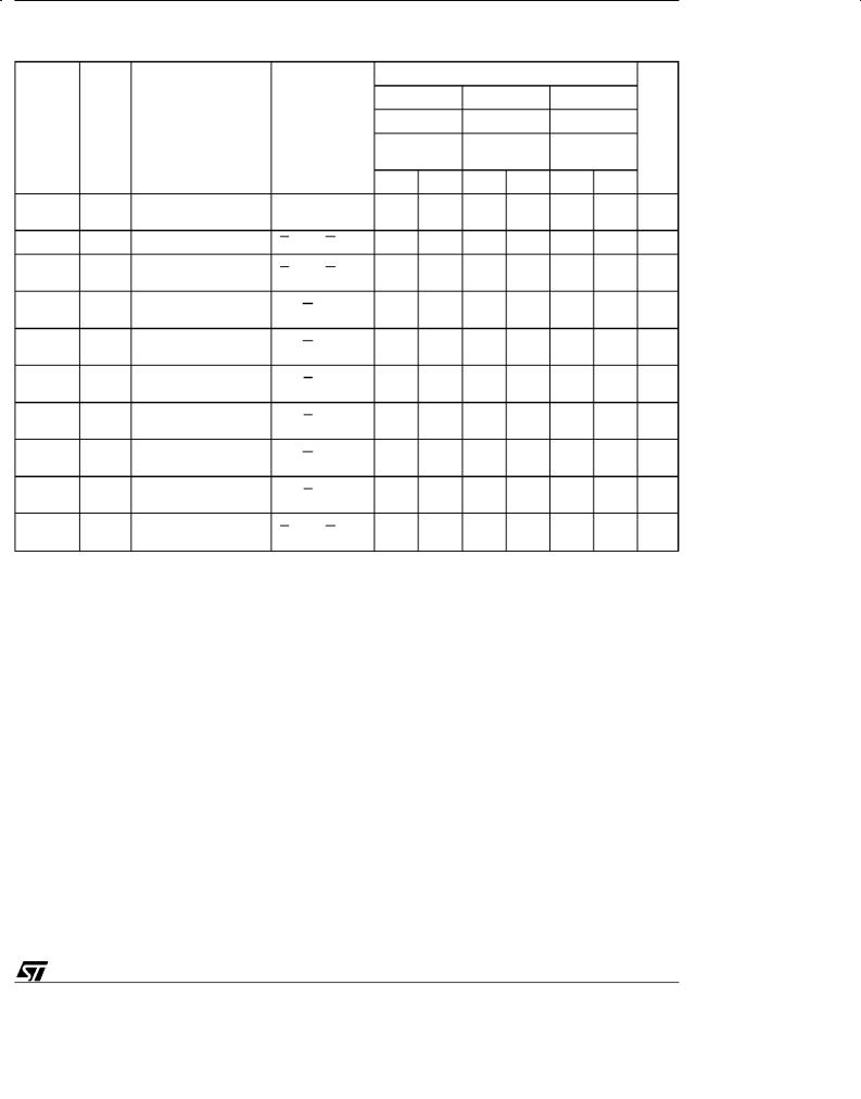
Table 9A. Read Only Mode AC Characteristics
(TA = 0 to 70 °C, ±40 to 85 °C or ±40 to 125 °C; 0V ≤ VPP ≤ 6.5V)
|
|
|
|
|
|
M28F101 |
|
|
|
|
|
|
|
|
|
-70 |
|
-90 |
-100 |
|
|
Symbol |
Alt |
Parameter |
Test Condition |
VCC=5V±5% VCC=5V±10% VCC=5V±10% |
Unit |
|||||
|
|
|
|
|
||||||
|
|
|
|
SRAM |
EPROM |
EPROM |
|
|||
|
|
|
|
Interface |
Interface |
Interface |
|
|||
|
|
|
|
Min |
Max |
Min |
Max |
Min |
Max |
|
tWHGL |
|
Write Enable High to |
|
6 |
|
6 |
|
6 |
|
μs |
|
Output Enable Low |
|
|
|
|
|||||
|
|
|
|
|
|
|
|
|
|
|
tAVAV |
tRC |
Read Cycle Time |
E = VIL, G = VIL |
70 |
|
90 |
|
100 |
|
ns |
tAVQV |
tACC |
Address Valid to |
E = VIL, G = VIL |
|
70 |
|
90 |
|
100 |
ns |
Output Valid |
|
|
|
|||||||
|
|
|
|
|
|
|
|
|
|
|
(1) |
tLZ |
Chip Enable Low to |
G = VIL |
0 |
|
0 |
|
0 |
|
ns |
tELQX |
Output Transition |
|
|
|
||||||
|
|
|
|
|
|
|
|
|
|
|
tELQV |
tCE |
Chip Enable Low to |
G = VIL |
|
70 |
|
90 |
|
100 |
ns |
Output Valid |
|
|
|
|||||||
|
|
|
|
|
|
|
|
|
|
|
(1) |
tOLZ |
Output Enable Low to |
E = VIL |
0 |
|
0 |
|
0 |
|
ns |
tGLQX |
Output Transition |
|
|
|
||||||
|
|
|
|
|
|
|
|
|
|
|
tGLQV |
tOE |
Output Enable Low to |
E = VIL |
|
40 |
|
40 |
|
45 |
ns |
Output Valid |
|
|
|
|||||||
|
|
|
|
|
|
|
|
|
|
|
(1) |
|
Chip Enable High to |
G = VIL |
0 |
30 |
0 |
45 |
0 |
45 |
ns |
tEHQZ |
|
Output Hi-Z |
||||||||
|
|
|
|
|
|
|
|
|
|
|
(1) |
tDF |
Output Enable High to |
E = VIL |
0 |
30 |
0 |
30 |
0 |
30 |
ns |
tGHQZ |
Output Hi-Z |
|||||||||
|
|
|
|
|
|
|
|
|
|
|
tAXQX |
tOH |
Address Transition to |
E = VIL, G = VIL |
0 |
|
0 |
|
0 |
|
ns |
Output Transition |
|
|
|
|||||||
|
|
|
|
|
|
|
|
|
|
|
Note: 1. Sampled only, not 100% tested
Read Mode. The Read Mode is the default at power up or may be set-up by writing 00h to the command register. Subsequent read operations output data from the memory. The memory remains in the Read Mode until a new command is written to the command register.
Electronic Signature Mode. In order to select the correct erase and programming algorithms for onboard programming, the manufacturer and device
codes may be read directly. It is not neccessary to apply a high voltage to A9 when using the command register. The Electronic Signature Mode is set-up by writing 90h to the command register. The following read cycles, with address inputs 00000h or 00001h, output the manufacturer or device type codes. The command is terminated by writing another valid command to the command register (for example Reset).
7/23
 Loading...