


ST72E311J4D0
SGS Thomson Microelectronics ST72E311J4D0, ST72E331N4D0S, ST72E331N4D0, ST72E331J4D0S, ST72E331J4D0 Datasheet
September 1999 1/106
ST72E331
ST72T331
8-BIT MCU WITH 8 TO 16K OTP/EPROM, 256 EEPROM,
384 TO 512 BYTES RAM, ADC, WDG, SCI, SPI AND 2 TIMERS
DATASHEET
■ User Program Memory (OTP/EPROM):
8 to16K bytes
■ User EEPROM: 256 bytes
■ Data RAM: 384 to512 bytesincluding 256 bytes
of stack
■ Master Resetand Power-On Reset
■ Low Voltage Detector (LVD) Reset option
■ Run andPower Saving modes
■ 44 or32 multifunctional bidirectional I/O lines:
– 15 or 9 programmable interrupt inputs
– 8 or 4 high sink outputs
– 8 or 6 analog alternate inputs
– 13 alternate functions
– EMI filtering
■ Software or Hardware Watchdog (WDG)
■ Two 16-bit Timers, each featuring:
– 2 Input Captures
1)
– 2 Output Compares
1)
– External Clock input (on Timer A)
– PWM and Pulse Generator modes
■ Synchronous Serial Peripheral Interface (SPI)
■ Asynchronous Serial Communications Interface
(SCI)
■ 8-bit ADC with 8 channels
2)
■ 8-bit Data Manipulation
■ 63 basic Instructions and 17 main Addressing
Modes
■ 8 x8 Unsigned Multiply Instruction
■ True BitManipulation
■ Complete Development Support on DOS/
WINDOWS
TM
Real-Time Emulator
■ Full Software Package on DOS/WINDOWS
TM
(C-Compiler, Cross-Assembler, Debugger)
Notes:
1. One only on Timer A.
2. Six channels only for ST72T331J.
Device Summary
Note: The ROM versions are supportedby the ST72334 family.
TQFP44
PSDIP42
PSDIP56
CSDIP42W
CSDIP56W
TQFP64
(See ordering information at the end of datashee
Features ST72T331J2 ST72T331J4 ST72T331N2 ST72T331N4
Program Memory - bytes 8K 16K 8K 16K
EEPROM - bytes 256
RAM (stack) - bytes 384 (256) 512 (256) 384 (256) 512 (256)
Peripherals Watchdog, Timers, SPI, SCI, ADC and optional Low Voltage Detector Reset
Operating Supply 3 to 5.5 V
CPU Frequency 8MHz max (16MHz oscillator) - 4MHz max over 85°C
Temperature Range - 40°C to + 125°C
Package TQFP44 -SDIP42 TQFP64 -SDIP56
1
Rev. 1.7

2/106
Table of Contents
95
ST72E331/ST72T331 . . . . . . . . . . . .......................1
1 GENERAL DESCRIPTION . . . . . . ................................................ 5
1.1 INTRODUCTION . . . . . . . . . . . . . ............................................ 5
1.2 PIN DESCRIPTION . . ..................................................... 6
1.3 EXTERNAL CONNECTIONS . . . . . . . . . .. . . . . . . . . . . .. . . . . . . . . . . . . . . . . ........ 10
1.4 MEMORY MAP . . . .. . . . . . ............................................... 11
1.5 OPTION BYTE . . . . .. ....................................................14
2 CENTRAL PROCESSING UNIT . . ............................................... 15
2.1 INTRODUCTION . . . . . . . . . . . . . ...........................................15
2.2 MAIN FEATURES . . . .. . . . . . .. . . . . . . . . . . . . ............................... 15
2.3 CPU REGISTERS . . . .................................................... 15
3 CLOCKS, RESET, INTERRUPTS & POWER SAVING MODES . . . . . .. . . . . . . ........... 18
3.1 CLOCK SYSTEM . . . . . .. . . . . . . ...........................................18
3.1.1 General Description . . . .. ............................................18
3.1.2 External Clock . . . . . . . . . . . . . ........................................ 18
3.2 RESET . . . . . . . . . . .. .. . . . . . . . . . . .. .. . . . . . ............................... 19
3.2.1 Introduction . . . .................................................... 19
3.2.2 External Reset . . . . . . ...............................................19
3.2.3 Reset Operation . . . . . . . . . . . . . . .. . . . . . . . .. ........................... 19
3.2.4 Low Voltage DetectorReset . . . . . . . . . . . . . . .. . . . . . . .. . . . . . . .. . . . . . . . . . . 20
3.3 INTERRUPTS . . . .. . . . . . . . . . . . . . . . . . . . . . . . . . . . .. . . . . . . . . .. . . . . . . . . .. . . . . 21
3.4 POWER SAVING MODES . . . . . . . . . . . . . . . . . . . . . . . .. . . . . . . . . . . .. . . . . ........ 24
3.4.1 Introduction . . . .................................................... 24
3.4.2 Slow Mode . . .. . . . . . . . . . . . . . . . . . . . ................................. 24
3.4.3 Wait Mode . . . . . . . . .. . . . . . . ........................................ 24
3.4.4 Halt Mode . . . . . .................................................... 25
3.5 MISCELLANEOUS REGISTER . . . . .. .. . . . ..................................26
4 ON-CHIP PERIPHERALS . . . . . . . . . . . ...........................................27
4.1 I/O PORTS . . . . . . . . . . . . . . . . . . ........................................... 27
4.1.1 Introduction . . . .................................................... 27
4.1.2 Functional Description . . . . ...........................................27
4.1.3 I/O Port Implementation . . . . . . . . . . . . . . .. . . . ........................... 28
4.1.4 Register Description . . . . . . ...........................................31
4.2 EEPROM(EEP)......................................................... 33
4.2.1 Introduction . . . .................................................... 33
4.2.2 Main Features . .. .. . ...............................................33
4.2.3 Functional description . . .. . . . . . .. . . . . . . . . . ........................... 34
4.2.4 Low Power Modes . . . ............................................... 36
4.2.5 Interrupts . . . . . .. . . . . . . . . . . . . . . . . . ................................. 36
4.2.6 Register Description . . . . . . ...........................................36
4.3 WATCHDOG TIMER (WDG) . . . . . . . . . . . . . . . . . . . . . . . . . . . . . . . . . . .. . . . . . . . . . . . 37
4.3.1 Introduction . . . .................................................... 37
4.3.2 Main Features . .. .. . ...............................................37
4.3.3 Functional Description . . . . ...........................................37
4.3.4 Hardware Watchdog Option . .. . . . . . . . ................................. 38
2

3/106
Table of Contents
4.3.5 Low Power Modes . . . ............................................... 38
4.3.6 Interrupts . . . . . .. . . . . . . . . . . . . . . . . . ................................. 38
4.3.7 Register Description . . . . . . ...........................................38
4.4 16-BIT TIMER . . . . . . . .. . . . . . . . .. ........................................40
4.4.1 Introduction . . . .................................................... 40
4.4.2 Main Features . .. .. . ...............................................40
4.4.3 Functional Description . . . . ...........................................40
4.4.4 Low Power Modes . . ............................................... 51
4.4.5 Interrupts . . .. . ....................................................51
4.4.6 Register Description . . . . . . ...........................................52
4.5 SERIAL COMMUNICATIONS INTERFACE (SCI) . . . . . . . . . . . . . . . . . . . . . . . . . .. . . . . 57
4.5.1 Introduction . . . .................................................... 57
4.5.2 Main Features . .. .. . ...............................................57
4.5.3 General Description . . . .. ............................................57
4.5.4 Functional Description . . . . ...........................................59
4.5.5 Low Power Modes . . . ............................................... 64
4.5.6 Interrupts . . . . . .. . . . . . . . . . . . . . . . . . ................................. 64
4.5.7 Register Description . . . . . . ...........................................65
4.6 SERIAL PERIPHERAL INTERFACE (SPI) . . . . . . . . . . .. . . . . . . . . . . . . ............69
4.6.1 Introduction . . . .................................................... 69
4.6.2 Main Features . .. .. . ...............................................69
4.6.3 General description . . . . . . . . . . . . . . . . .. . . .. . . . . . . . . . . . . . . . . . . . . . . . . . . . 69
4.6.4 Functional Description . . . . ...........................................71
4.6.5 Low Power Modes . . . ............................................... 78
4.6.6 Interrupts . . .. . ....................................................78
4.6.7 Register Description . . . . . . ...........................................79
4.7 8-BIT A/D CONVERTER (ADC) . . . . . .. .. . . . . . . . . . ........................... 82
4.7.1 Introduction . . . .................................................... 82
4.7.2 Main Features . .. .. . ...............................................82
4.7.3 Functional Description . . . . ...........................................83
4.7.4 Low Power Modes . . . ............................................... 83
4.7.5 Interrupts . . . . . .. . . . . . . . . . . . . . . . . . ................................. 83
4.7.6 Register Description . . . . . . ...........................................84
5 INSTRUCTION SET .. . . . . . . . . . . . . . . . . ........................................ 85
5.1 ST7 ADDRESSING MODES . . . . . . . . . .. . . . . . . . . . . . . . . . . . . . . . . . .. . . . . . . . . . . . 85
5.1.1 Inherent . . . . . . . . . . . ...............................................86
5.1.2 Immediate . .. . . . .. . . . . . . . .. . . . . . . . . . . . . . .. . . . . . . .. . . . . . . . . . . . . . . . . 86
5.1.3 Direct . ........................................................... 86
5.1.4 Indexed (No Offset, Short, Long) . . . . . . . . . . . . ........................... 86
5.1.5 Indirect (Short, Long) . . . . .. . . . . . . . . . .. . . . . . . . . . . . . . . . . . . . . . . .. . . . . . . . 86
5.1.6 Indirect Indexed (Short,Long) . ........................................87
5.1.7 Relative mode (Direct,Indirect) . . . .. . . . . . . . .. . . . . . . . . . . .. . . . . . . . . . .. . . . 87
5.2 INSTRUCTION GROUPS . . .. . . . . . . . . . . .. ................................. 88
6 ELECTRICALCHARACTERISTICS . . . . . . . . .. . . . . . . .............................. 91
6.1 ABSOLUTE MAXIMUM RATINGS . . . ........................................91
6.2 RECOMMENDED OPERATING CONDITIONS . . . .............................. 92
6.3 RESET CHARACTERISTICS . . . . . . . . . . .................................... 93
3

4/106
ST72E331 ST72T331
6.4 OSCILLATOR CHARACTERISTICS . . . . . . . . . . ............................... 93
6.5 DC ELECTRICAL CHARACTERISTICS . . . . . .. . . . .. . . . . . . . .. . . . . . . ...........94
6.6 PERIPHERAL CHARACTERISTICS . . . . . . . ..................................95
7 GENERAL INFORMATION . . . . . . . . . . ..........................................101
7.1 EPROM ERASURE . . .. . . . . . . . . . . .. .. . . . . . . ............................. 101
7.2 PACKAGE MECHANICALDATA . . .. . . . . . . . . . . . . . .......................... 102
7.3 ORDERING INFORMATION . . . . . .. . . . .. . ................................. 105
8 SUMMARY OF CHANGES . . . . . . . . . . . . . . . . . . . . . . . . . . . . . . . . . . . . . . . . . . . . . . . . . . . . 106
4
5/106
ST72E331 ST72T331
1 GENERAL DESCRIPTION
1.1 INTRODUCTION
The ST72T331 HCMOS Microcontroller Unit
(MCU) is a member of the ST7 family.The device
is based on an industry-standard 8-bit core and
features an enhanced instruction set. The device
is normally operated at a 16 MHz oscillator fre-
quency. Under software control, the ST72T331
may be placed in either Wait, Slow or Halt modes,
thus reducing power consumption. The enhanced
instruction set and addressing modes afford real
programming potential. In addition to standard
8-bit data management, the ST72T331 features
true bit manipulation, 8x8 unsigned multiplication
and indirect addressing modeson the whole mem-
ory. The device includes a low consumption and
fast start on-chip oscillator, CPU, program memo-
ry (OTP/EPROM versions), EEPROM, RAM, 44
(QFP64 and SDIP56) or 32 (QFP44 and SDIP42)
I/O lines, a Low Voltage Detector (LVD) and the
following on-chip peripherals: Analog-to-Digital
converter (ADC) with 8 (QFP64, SDIP56) or 6
(QFP44, SDIP42) multiplexed analog inputs, in-
dustry standard synchronous SPI and asynchro-
nous SCI serial interfaces, digital Watchdog, two
independent 16-bit Timers, one featuring an Exter-
nal Clock Input, and both featuring Pulse Genera-
tor capabilities, 2 Input Captures and 2 Output
Compares (only 1 Input Capture and 1 Output
Compare on Timer A).
Figure 1. ST72T331 Block Diagram
8-BIT CORE
ALU
ADDRESS AND DATA BUS
OSCIN
OSCOUT
RESET
PORT B
TIMER B
PORT C
SPI
PORT E
SCI
PORT D
8-BIT ADC
WATCHDOG
PB0 -> PB7
PC0 -> PC7
PE0 -> PE7
PD0 -> PD7
OSC
Internal
CLOCK
CONTROL
RAM
(384 - 512 Bytes)
PORT F
PF0 -> PF2,4,6,7
TIMER A
PORT A
PA0 -> PA7
V
SSA
V
DDA
(6 bits forST72T331N)
(6 bits)
EEPROM
(256 Bytes)
AND LVD
(2 bits for ST72T331J)
(8 bits for ST72T331N)
(6 bits for ST72T331J)
(8 bits for ST72T331N)
(5 bits for ST72T331J)
(8 bits)
(8 bits for ST72T331N)
(5 bits for ST72T331J)
V
SS
V
DD
POWER
SUPPLY
PROGRAM
(8 - 16K Bytes)
MEMORY
5
6/106
ST72E331 ST72T331
1.2 PIN DESCRIPTION
Figure 2. 64-Pin Thin QFP Package Pinout
Figure 3. 56-Pin Shrink DIPPackage Pinout
Figure 4. 44-Pin Thin QFP Package Pinout
Figure 5. 42-Pin Shrink DIP Package Pinout
1
2
3
4
5
6
7
8
9
10
11
12
13
14
15
16
48
47
46
45
44
43
42
41
40
39
38
37
36
35
34
33
64 6362 6160 5958 5756 55 54 53 5251 50 49
17 18192021 2223 24 29 30313225 262728
PE4
PE5
PE6
PE7
PB0
PB1
PB2
PB3
PB4
PB5
PB6
PB7
AIN0/PD0
AIN1/PD1
AIN2/PD2
AIN3/PD3
V
SS_1
V
DD_1
PA3
PA2
PA1
PA0
PC7/SS
PC6/SCK
PC5/MOSI
PC4/MISO
PC3/ICAP1_B
PC2/ICAP2_B
PC1/OCMP1_B
PC0/OCMP2_B
V
SS_0
V
DD_0
AIN4/PD4
AIN5/PD5
AIN6/PD6
AIN7/PD7
V
DDA
V
SSA
V
DD_3
V
SS_3
CLKOUT/PF0
PF1
PF2
NC
OCMP1_A/PF4
NC
ICAP1_A/PF6
EXTCLK_A/PF7
NC
NC
PE1/RDI
PE0/TDO
V
DD_2
OSCIN
OSCOUT
V
SS_2
NC
NC
RESET
TEST/V
PP
1)
PA7
PA6
PA5
PA4
(EI0)
(EI0)
(EI0)
(EI0)
(EI2)
(EI2)
(EI2)
(EI2)
(EI3)
(EI3)
(EI3)
(EI3)
(EI1)
(EI1)
(EI1)
1. V
PP
on EPR OM/OTP only
15 (EI1)
16 (EI1)
17 (EI1)
18
19
20
21
22
23
24
25
26
27
28 29
30
(EI0) 31
(EI0) 32
(EI0) 33
(EI0) 34
CLKOUT/PF0
PF1
PF2
OCMP1_A/PF4
ICAP1_A/PF6
PC1/OCMP1_B
PC2/ICAP2_B
EXTCLK_A/PF7
V
DD_0
V
SS_0
RESET
TEST/V
PP
1)
PA7
PA6
PA5
PA2
PA1
PA0
PC7/SS
PC6/SCK
42
41
40
39
38
37
36
35
PC0/OCMP2_B
PC3/ICAP1_B
PC4/MISO
PC5/MOSI
PA4
V
SS_1
V
DD_1
PA3
1 (EI3)
2 (EI3)
3 (EI3)
4 (EI3)
5
6
7
8
9
10
11
12
13
14
43
44
45
46
47
48
PB4
PB5
PB6
PB7
AIN0/PD0
AIN5/PD5
AIN6/PD6
AIN1/PD1
AIN2/PD2
AIN3/PD3
PB3
PB2
PB1
PB0
PE7
PE0/TD0
V
DD_2
OSCIN
OSCOUT
V
SS_2
(EI2) 56
(EI2) 55
(EI2) 54
(EI2) 53
52
51
50
49
AIN4/PD4
AIN7/PD7
V
DDA
V
SSA
PE6
PE5
PE4
PE1/RDI
1.V
PP
on EPROM/OTP only
1
2
3
4
5
6
7
8
9
10
11
33
32
31
30
29
28
27
26
25
24
23
44 43 42 41 40 39 38 37 36 35 34
12 13 14 15 16 17 18 19
(EI1)
(EI1)
(EI1)
20 21 22
CLKOUT/PF0
PF1
PF2
OCMP1_A/PF4
ICAP1_A/PF6
PC1/OCMP1_B
PC2/ICAP2_B
EXTCLK_A/PF7
V
DD_0
V
SS_0
PC0/OCMP2_B
PC3/ICAP1_B
PC4/MISO
PC5/MOSI
PB4
AIN0/PD0
AIN5/PD5
AIN1/PD1
AIN2/PD2
AIN3/PD3
AIN4/PD4
V
DDA
V
SSA
RESET
TEST/V
PP
1)
PA7
PA6
PA5
PC7/SS
PC6/SCK
PA4
V
SS_1
V
DD_1
PA3
PB3
PB2
PB1
PB0
PE0/TD0
V
DD_2
OSCIN
OSCOUT
V
SS_2
PE1/RDI
(EI3)
(EI2)
(EI2)
(EI2)
(EI2)
(EI0)
1. V
PP
on EPROM/OTP only
15
16
17
18
19
20
21
CLKOUT/PF0
PF1
PF2
OCMP1_A/PF4
ICAP1_A/PF6
PC1/OCMP1_B
PC2/ICAP2_B
EXTCLK_A/PF7
RESET
TEST/V
PP
1)
PA7
PA6
PA5
PC7/SS
PC6/SCK
28
27
26
25
24
23
22
PC0/OCMP2_B
PC3/ICAP1_B
PC4/MISO
PC5/MOSI
PA4
V
SS_1
V
DD_1
PA3
1
2
3
4
5
6
7
8
9
10
11
12
13
14
29
30
31
32
33
34
PB4
AIN0/PD0
AIN5/PD5
AIN1/PD1
AIN2/PD2
AIN3/PD3
PB3
PB2
PB1
PB0
PE0/TD0
V
DD_2
OSCIN
OSCOUT
V
SS_2
42
41
40
39
38
37
36
35
AIN4/PD4
V
DDA
V
SSA
PE1/RDI
(EI3)
(EI1)
(EI1)
(EI1)
(EI0)
(EI2)
(EI2)
(EI2)
(EI2)
1. V
PP
on EPROM/OTP only
6

7/106
ST72E331 ST72T331
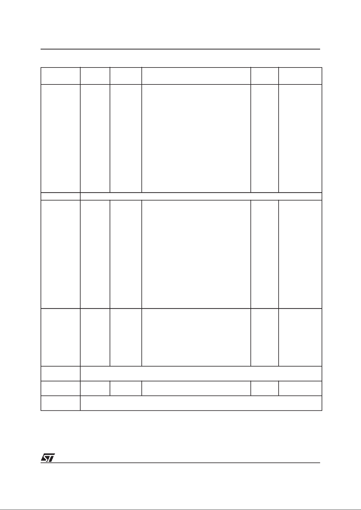
Table 1. ST72T331Nx Pin Description
Pin n°
QFP64
Pin n°
SDIP56
Pin Name Type Description Remarks
1 49 PE4 I/O Port E4 High Sink
2 50 PE5 I/O Port E5 High Sink
3 51 PE6 I/O Port E6 High Sink
4 52 PE7 I/O Port E7 High Sink
5 53 PB0 I/O Port B0 External Interrupt: EI2
6 54 PB1 I/O Port B1 External Interrupt: EI2
7 55 PB2 I/O Port B2 External Interrupt: EI2
8 56 PB3 I/O Port B3 External Interrupt: EI2
9 1 PB4 I/O Port B4 External Interrupt: EI3
10 2 PB5 I/O Port B5 External Interrupt: EI3
11 3 PB6 I/O Port B6 External Interrupt: EI3
12 4 PB7 I/O Port B7 External Interrupt: EI3
13 5 PD0/AIN0 I/O Port D0 or ADC Analog Input 0
14 6 PD1/AIN1 I/O Port D1 or ADC Analog Input 1
15 7 PD2/AIN2 I/O Port D2 or ADC Analog Input 2
16 8 PD3/AIN3 I/O Port D3 or ADC Analog Input 3
17 9 PD4/AIN4 I/O Port D4 or ADC Analog Input 4
18 10 PD5/AIN5 I/O Port D5 or ADC Analog Input 5
19 11 PD6/AIN6 I/O Port D6 or ADC Analog Input 6
20 12 PD7/AIN7 I/O Port D7 or ADC Analog Input 7
21 13 V
DDA
S Power Supply for analog peripheral (ADC)
22 14 V
SSA
S Ground for analog peripheral (ADC)
23 V
DD_3
S Main power supply
24 V
SS_3
S Ground
25 15 PF0/CLKOUT I/O Port F0 or CPU Clock Output External Interrupt: EI1
26 16 PF1 I/O Port F1 External Interrupt: EI1
27 17 PF2 I/O Port F2 External Interrupt: EI1
28 NC Not Connected
29 18 PF4/OCMP1_A I/O Port F4 or Timer A Output Compare 1
30 NC Not Connected
31 19 PF6/ICAP1_A I/O Port F6 or Timer AInput Capture 1
32 20 PF7/EXTCLK_A I/O Port F7 or External Clock on Timer A
33 21 V
DD_0
S Main power supply
34 22 V
SS_0
S Ground
35 23 PC0/OCMP2_B I/O Port C0 or Timer B Output Compare 2
36 24 PC1/OCMP1_B I/O Port C1 or Timer B Output Compare 1
37 25 PC2/ICAP2_B I/O Port C2 or Timer B Input Capture 2
38 26 PC3/ICAP1_B I/O Port C3 or Timer B Input Capture 1
39 27 PC4/MISO I/O Port C4 or SPI Master In/ Slave Out Data
40 28 PC5/MOSI I/O Port C5 or SPI Master Out/ Slave In Data
41 29 PC6/SCK I/O Port C6 or SPI Serial Clock
42 30 PC7/SS I/O Port C7 or SPI Slave Select
43 31 PA0 I/O Port A0 External Interrupt: EI0
7
8/106
ST72E331 ST72T331
Note 1:V
PP
on EPROM/OTP only.
Table 2. ST72T331Jx Pin Description
44 32 PA1 I/O Port A1 External Interrupt: EI0
45 33 PA2 I/O Port A2 External Interrupt: EI0
46 34 PA3 I/O Port A3 External Interrupt: EI0
47 35 V
DD_1
S Main power supply
48 36 V
SS_1
S Ground
49 37 PA4 I/O Port A4 High Sink
50 38 PA5 I/O Port A5 High Sink
51 39 PA6 I/O Port A6 High Sink
52 40 PA7 I/O Port A7 High Sink
53 41 TEST/V
PP
1)
S
Test mode pin . In the EPROM programming
mode, thispin acts as the programming voltage
input V
PP.
This pin must be tied
low in user mode
54 42 RESET I/O Bidirectional. Active low. Top priority non maskable interrupt.
55 NC Not Connected
56 NC Not Connected
57 43 V
SS_2
S Ground
58 44 OSCOUT O
Input/Output Oscillator pin. These pins connect a parallel-resonant
crystal, or an external source to theon-chip oscillator.
59 45 OSCIN I
60 46 V
DD_2
S Main power supply
61 47 PE0/TDO I/O Port E1 or SCI Transmit Data Out
62 48 PE1/RDI I/O Port E1 or SCI Receive Data In
63 NC Not Connected
64 NC Not Connected
Pin n°
QFP64
Pin n°
SDIP56
Pin Name
Type
Description Remarks
Pin n°
QFP44
Pin n°
SDIP42
Pin Name Type Description Remarks
1 38 PE1/RDI I/O Port E1 or SCI Receive Data In
2 39 PB0 I/O Port B0 External Interrupt: EI2
3 40 PB1 I/O Port B1 External Interrupt: EI2
4 41 PB2 I/O Port B2 External Interrupt: EI2
5 42 PB3 I/O Port B3 External Interrupt: EI2
6 1 PB4 I/O Port B4 External Interrupt: EI3
7 2 PD0/AIN0 I/O Port D0 or ADC Analog Input 0
8 3 PD1/AIN1 I/O Port D1 or ADC Analog Input 1
9 4 PD2/AIN2 I/O Port D2 or ADC Analog Input 2
10 5 PD3/AIN3 I/O Port D3 or ADC Analog Input 3
11 6 PD4/AIN4 I/O Port D4 or ADC Analog Input 4
12 7 PD5/AIN5 I/O Port D5 or ADC Analog Input 5
13 8 V
DDA
S Power Supply for analog peripheral (ADC)
14 9 V
SSA
S Ground for analog peripheral (ADC)
15 10 PF0/CLKOUT I/O Port F0 or CPU Clock Output External Interrupt: EI1
16 11 PF1 I/O Port F1 External Interrupt: EI1
17 12 PF2 I/O Port F2 External Interrupt: EI1
8
9/106
ST72E331 ST72T331
Note 1:V
PP
on EPROM/OTP only.
18 13 PF4/OCMP1_A I/O Port F4 or Timer A Output Compare 1
19 14 PF6/ICAP1_A I/O Port F6 or Timer A Input Capture 1
20 15 PF7/EXTCLK_A I/O Port F7 or External Clock on Timer A
21 V
DD_0
S Main power supply
22 V
SS_0
S Ground
23 16 PC0/OCMP2_B I/O Port C0 or Timer B Output Compare 2
24 17 PC1/OCMP1_B I/O Port C1 or Timer B Output Compare 1
25 18 PC2/ICAP2_B I/O Port C2 or Timer B Input Capture 2
26 19 PC3/ICAP1_B I/O Port C3 or Timer B Input Capture 1
27 20 PC4/MISO I/O Port C4 or SPI Master In / Slave Out Data
28 21 PC5/MOSI I/O Port C5 or SPI Master Out / Slave In Data
29 22 PC6/SCK I/O Port C6or SPI Serial Clock
30 23 PC7/SS I/O Port C7 or SPI Slave Select
31 24 PA3 I/O Port A3 External Interrupt: EI0
32 25 V
DD_1
S Main power supply
33 26 V
SS_1
S Ground
34 27 PA4 I/O Port A4 High Sink
35 28 PA5 I/O Port A5 High Sink
36 29 PA6 I/O Port A6 High Sink
37 30 PA7 I/O Port A7 High Sink
38 31 TEST/V
PP
1)
S
Test mode pin. In the EPROM programming
mode, this pin acts as the programming
voltage input V
PP.
This pin must be tied
low in user mode
39 32 RESET I/O Bidirectional. Active low. Top priority nonmaskable interrupt.
40 33 V
SS_2
S Ground
41 34 OSCOUT O
Input/Output Oscillator pin. These pins connect a parallel-resonant
crystal, or an external source to the on-chip oscillator.
42 35 OSCIN I
43 36 V
DD_2
S Main power supply
44 37 PE0/TDO I/O Port E0or SCI Transmit Data Out
Pin n°
QFP44
Pin n°
SDIP42
Pin Name Type Description Remarks
9
10/106
ST72E331 ST72T331
1.3 EXTERNAL CONNECTIONS
The following figure shows the recommended ex-
ternal connections for the device.
The V
PP
pin is only used for programming OTP
and EPROM devices and must betied to ground in
user mode.
The 10 nF and 0.1 µF decoupling capacitors on
the power supply lines are a suggested EMC per-
formance/cost tradeoff.
The external reset network is intended to protect
the device against parasitic resets, especially in
noisy environments.
Unused I/Os should be tied high to avoid any un-
necessary power consumption on floating lines.
An alternative solution is to program the unused
ports as inputs with pull-up.
Figure 6. Recommended External Connections
V
PP
V
DD
V
SS
OSCIN
OSCOUT
RESET
V
DD
0.1µF
+
See
Clocks
Section
V
DD
0.1µF
0.1µF
EXTERNAL RESET CIRCUIT
Or configure unused I/O ports
Unused I/O
10nF
4.7K
10K
by software as input with pull-up
V
DD
V
DDA
V
SSA
See
A/D Converter
Section
Detector (LVD) is used
Optional if Low Voltage
10
11/106
ST72E331 ST72T331
1.4 MEMORY MAP
Figure 7. Program Memory Map
Table 3. Interrupt Vector Map
Vector Address Description Remarks
FFE0-FFE1h
FFE2-FFE3h
FFE4-FFE5h
FFE6-FFE7h
FFE8-FFE9h
FFEA-FFEBh
FFEC-FFEDh
FFEE-FFEFh
FFF0-FFF1h
FFF2-FFF3h
FFF4-FFF5h
FFF6-FFF7h
FFF8-FFF9h
FFFA-FFFBh
FFFC-FFFDh
FFFE-FFFFh
Not Used
Not Used
EEPROM Interrupt Vector
SCI Interrupt Vector
TIMER B Interrupt Vector
TIMER A Interrupt Vector
SPI interrupt vector
Not Used
External Interrupt Vector EI3
External Interrupt Vector EI2
External Interrupt Vector EI1
External Interrupt Vector EI0
Not Used
Not Used
TRAP (software) Interrupt Vector
RESET Vector
Internal Interrupt
Internal Interrupt
Internal Interrupt
Internal Interrupt
Internal Interrupt
External Interrupt
External Interrupt
External Interrupt
External Interrupt
CPU Interrupt
0000h
Interrupt & Reset Vectors
HW Registers
027Fh
0080h
Short Addressing
RAM (zero page)
16-bit Addressing
RAM
007Fh
0200h / 0280h
0BFFh
Reserved
0080h
(see Table 4)
0C00h
FFDFh
FFE0h
FFFFh
(see Table 3)
027Fh
C000h
Reserved
EEPROM256 Bytes
0CFFh
0D00h
BFFFh
00FFh
0100h
01FFh
0200h
8K Bytes
E000h
16K Bytes
Program
Short Addressing
RAM (zero page)
0080h
00FFh
01FFh
01FFh
384 Bytes RAM
512 Bytes RAM
256 Bytes Stack/
16-bit Addressing RAM
256 Bytes Stack/
16-bit Addressing RAM
0100h
Memory
Program
Memory
11
12/106
ST72E331 ST72T331
Table 4. Hardware Register Memory Map
Address Block
Register
Label
Register Name
Reset
Status
Remarks
0000h
0001h
0002h
Port A
PADR
PADDR
PAOR
Data Register
Data Direction Register
Option Register
00h
00h
00h
R/W
R/W
R/W
1)
0003h Reserved Area (1 byte)
0004h
0005h
0006h
Port C
PCDR
PCDDR
PCOR
Data Register
Data Direction Register
Option Register
00h
00h
00h
R/W
R/W
R/W
0007h Reserved Area (1 byte)
0008h
0009h
000Ah
Port B
PBDR
PBDDR
PBOR
Data Register
Data Direction Register
Option Register
00h
00h
00h
R/W
R/W
R/W
1)
000Bh Reserved Area (1 byte)
000Ch
000Dh
000Eh
Port E
PEDR
PEDDR
PEOR
Data Register
Data Direction Register
Option Register
00h
00h
0Ch
R/W
R/W
R/W
1)
000Fh Reserved Area (1 byte)
0010h
0011h
0012h
Port D
PDDR
PDDDR
PDOR
Data Register
Data Direction Register
Option Register
00h
00h
00h
R/W
R/W
R/W
1)
0013h Reserved Area (1 byte)
0014h
0015h
0016h
Port F
PFDR
PFDDR
PFOR
Data Register
Data Direction Register
Option Register
00h
00h
28h
R/W
R/W
R/W
1)
0017h to
001Fh
Reserved Area (9 bytes)
0020h MISCR Miscellaneous Register 00h
0021h
0022h
0023h
SPI
SPIDR
SPICR
SPISR
SPI Data I/O Register
SPI Control Register
SPI Status Register
xxh
xxh
00h
R/W
R/W
Read Only
0024h to
0029h
Reserved Area (6 bytes)
002Ah
002Bh
WDG
WDGCR
WDGSR
Watchdog Control Register
Watchdog Status Register
7Fh
00h
R/W
R/W
3)
002Ch EEPROM EEPCR EEPROM Control Register 00h R/W Register
002Dh to
0030h
Reserved Area (4 bytes)
12
13/106
ST72E331 ST72T331
Notes:
1. The bits corresponding to unavailable pins are forcedto 1 by hardware, this affects the reset status value.
2. External pin not available.
3. Not used in versions without Low Voltage Detector Reset.
0031h
0032h
0033h
0034h-0035h
0036h-0037h
0038h-0039h
003Ah-003Bh
003Ch-003Dh
003Eh-003Fh
Timer A
TACR2
TACR1
TASR
TAIC1HR
TAIC1LR
TAOC1HR
TAOC1LR
TACHR
TACLR
TAACHR
TAACLR
TAIC2HR
TAIC2LR
TAOC2HR
TAOC2LR
Control Register2
Control Register1
Status Register
Input Capture1 High Register
Input Capture1 Low Register
Output Compare1 High Register
Output Compare1 Low Register
Counter High Register
Counter Low Register
Alternate Counter High Register
Alternate Counter Low Register
Input Capture2 High Register
Input Capture2 Low Register
Output Compare2 High Register
Output Compare2 Low Register
00h
00h
xxh
xxh
xxh
80h
00h
FFh
FCh
FFh
FCh
xxh
xxh
80h
00h
R/W
R/W
Read Only
Read Only
Read Only
R/W
R/W
Read Only
Read Only
Read Only
Read Only
Read Only
2)
Read Only
2)
R/W
2)
R/W
2)
0040h Reserved Area (1 byte)
0041h
0042h
0043h
0044h-0045h
0046h-0047h
0048h-0049h
004Ah-004Bh
004Ch-004Dh
004Eh-004Fh
Timer B
TBCR2
TBCR1
TBSR
TBIC1HR
TBIC1LR
TBOC1HR
TBOC1LR
TBCHR
TBCLR
TBACHR
TBACLR
TBIC2HR
TBIC2LR
TBOC2HR
TBOC2LR
Control Register2
Control Register1
Status Register
Input Capture1 High Register
Input Capture1 Low Register
Output Compare1 High Register
Output Compare1 Low Register
Counter High Register
Counter Low Register
Alternate Counter High Register
Alternate Counter Low Register
Input Capture2 High Register
Input Capture2 Low Register
Output Compare2 High Register
Output Compare2 Low Register
00h
00h
xxh
xxh
xxh
80h
00h
FFh
FCh
FFh
FCh
xxh
xxh
80h
00h
R/W
R/W
Read Only
Read Only
Read Only
R/W
R/W
Read Only
Read Only
Read Only
Read Only
Read Only
Read Only
R/W
R/W
0050h
0051h
0052h
0053h
0054h
0055h
0056h
0057h
SCI
SCISR
SCIDR
SCIBRR
SCICR1
SCICR2
SCIERPR
SCIETPR
SCI Status Register
SCI Data Register
SCI Baud Rate Register
SCI Control Register 1
SCI Control Register 2
SCI Extended Receive Prescaler Register
Reserved
SCI Extended Transmit Prescaler Register
C0h
xxh
00x----xb
xxh
00h
00h
---
00h
Read Only
R/W
R/W
R/W
R/W
R/W
Reserved
R/W
0058h to
006Fh
Reserved Area (24 bytes)
0070h
0071h
ADC
ADCDR
ADCCSR
ADC Data Register
ADC Control/Status Register
00h
00h
Read Only
R/W
0072h to
007Fh
Reserved Area (14 bytes)
Address Block
Register
Label
Register Name
Reset
Status
Remarks
13

14/106
ST72E331 ST72T331
1.5 OPTION BYTE
The user has the option to select software watch-
dog or hardware watchdog (see description in the
Watchdog chapter). When programming EPROM
or OTP devices, this option is selected in a menu
by the user of the EPROM programmer before
burning the EPROM/OTP. The Option Byte is lo-
cated in a non-user map. No address has to be
specified. TheOption Byte is atFFh after UVeras-
ure and must be properly programmed to set de-
sired options.
OPTBYTE
Bit 7:4 = Not used
Bit 3 = Reserved, must be cleared.
Bit 2 = Reserved, must be set onST72T331N de-
vices and mustbe cleared onST72T331J devices.
Bit 1 = Not used
Bit 0 = WDG
Watchdog disable
0: The Watchdog is enabled after reset (Hardware
Watchdog).
1: The Watchdog is not enabled after reset (Soft-
ware Watchdog).
70
- - - - b3 b2 - WDG
14
15/106
ST72E331 ST72T331
2 CENTRAL PROCESSING UNIT
2.1 INTRODUCTION
This CPU hasa full 8-bit architecture and contains
six internal registers allowing efficient 8-bit data
manipulation.
2.2 MAIN FEATURES
■ 63 basicinstructions
■ Fast 8-bit by 8-bit multiply
■ 17 main addressing modes (with indirect
addressing mode)
■ Two 8-bit index registers
■ 16-bit stackpointer
■ 8 MHzCPU internal frequency
■ Low power modes
■ Maskable hardware interrupts
■ Non-maskable software interrupt
2.3 CPU REGISTERS
The 6 CPU registers shown in Figure 8 are not
present in thememory mappingand are accessed
by specificinstructions.
Accumulator (A)
The Accumulator is an 8-bit general purpose reg-
ister used to hold operands and the results of the
arithmetic and logic calculations and to manipulate
data.
Index Registers (Xand Y)
In indexedaddressing modes, these 8-bitregisters
are used to create either effective addresses or
temporary storage areas for data manipulation.
(The Cross-Assembler generates a precede in-
struction (PRE) to indicate that the following in-
struction refers to the Y register.)
The Y register is notaffected by theinterrupt auto-
matic procedures (notpushed to and popped from
the stack).
Program Counter (PC)
The program counter is a 16-bit register containing
the address of the next instruction to be executed
by the CPU. It is made of two 8-bit registers PCL
(Program CounterLow which is the LSB) and PCH
(Program Counter High which is the MSB).
Figure 8. CPU Registers
ACCUMULATOR
X INDEX REGISTER
Y INDEX REGISTER
STACK POINTER
CONDITION CODE REGISTER
PROGRAM COUNTER
70
1C11HINZ
RESET VALUE= RESET VECTOR @ FFFEh-FFFFh
70
70
70
0
7
15 8
PCH
PCL
15
87 0
RESET VALUE = STACKHIGHER ADDRESS
RESET VALUE =
1X11X1XX
RESET VALUE = XXh
RESET VALUE= XXh
RESET VALUE= XXh
X = Undefined Value
15

16/106
ST72E331 ST72T331
CENTRAL PROCESSING UNIT (Cont’d)
CONDITION CODE REGISTER (CC)
Read/Write
Reset Value: 111x1xxx
The 8-bit Condition Code register contains the in-
terrupt mask and four flags representative of the
result of the instruction just executed. This register
can also be handled by the PUSH and POP in-
structions.
These bits can be individually tested and/or con-
trolled by specific instructions.
Bit 4 = H
Half carry
.
This bit isset by hardware when a carry occurs be-
tween bits 3 and 4 of the ALU during an ADD or
ADC instruction.It is reset by hardware during the
same instructions.
0: No half carry has occurred.
1: A half carry has occurred.
This bit is tested using the JRH or JRNH instruc-
tion. The H bit is useful in BCD arithmetic subrou-
tines.
Bit 3 = I
Interrupt mask
.
This bit is set by hardware when entering in inter-
rupt or by software to disable all interrupts except
the TRAP software interrupt. This bit is cleared by
software.
0: Interrupts are enabled.
1: Interrupts are disabled.
This bit is controlled by the RIM, SIM andIRET in-
structions andis tested by the JRM and JRNM in-
structions.
Note: Interrupts requested while I is set are
latched and can be processed when I is cleared.
By default an interrupt routine is not interruptable
because the I bit is set by hardware when youen-
ter it and reset by the IRET instruction at the end of
the interrupt routine. If the I bit is cleared by soft-
ware inthe interrupt routine, pending interrupts are
serviced regardless of the priority levelof the cur-
rent interrupt routine.
Bit 2 = N
Negative
.
This bit is set and cleared by hardware.It is repre-
sentative of the result sign of the last arithmetic,
logical or data manipulation. It is a copy of the 7
th
bit of the result.
0:The result of the lastoperation is positive or null.
1: The result of the last operation is negative
(i.e. the most significant bit is a logic 1).
This bit isaccessed by the JRMIand JRPL instruc-
tions.
Bit 1 = Z
Zero
.
This bit is set and clearedby hardware. Thisbit in-
dicates that the result of the last arithmetic, logical
or data manipulation is zero.
0: The result of the last operation is different from
zero.
1: The result of the last operation is zero.
This bit is accessed by the JREQ and JRNE test
instructions.
Bit 0 = C
Carry/borrow.
This bit is set and cleared by hardware and soft-
ware. It indicates an overflow or anunderflow has
occurred during the last arithmetic operation.
0: No overflowor underflow has occurred.
1: An overflow or underflow has occurred.
This bit is driven by the SCFand RCFinstructions
and tested by theJRC and JRNC instructions. It is
also affected by the “bit testand branch”, shift and
rotate instructions.
70
111HINZC
16
17/106
ST72E331 ST72T331
CENTRAL PROCESSING UNIT (Cont’d)
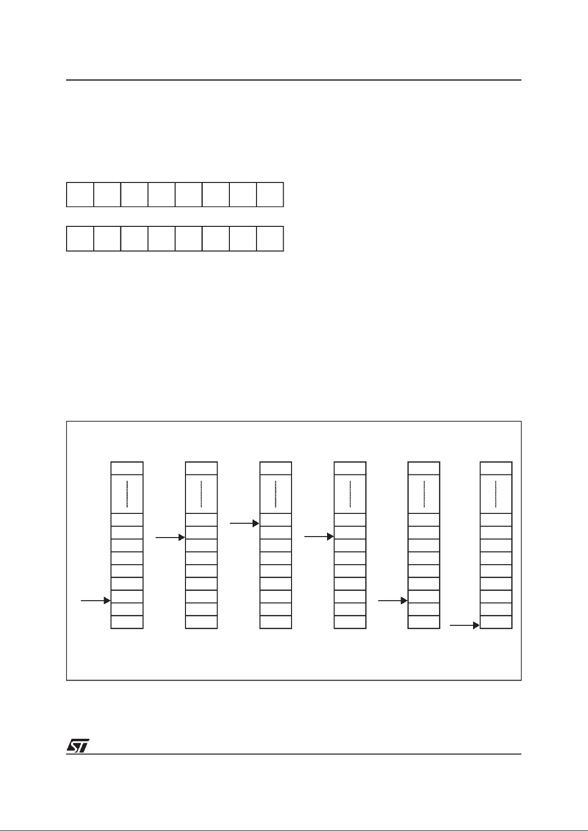
Stack Pointer (SP)
Read/Write
Reset Value: 01FFh
The Stack Pointer is a 16-bit register which is al-
ways pointingto thenext free location in the stack.
It isthen decremented after datahas been pushed
onto the stack and incremented before data is
popped from the stack (see Figure 9).
Since the stack is 256 bytes deep, the 8th most
significant bits are forced by hardware. Following
an MCU Reset, or after a Reset Stack Pointer in-
struction (RSP), the Stack Pointer contains its re-
set value (the SP7 to SP0 bits are set) which is the
stack higheraddress.
The least significant byte of the Stack Pointer
(called S) can be directly accessed by a LD in-
struction.
Note: When the lower limit is exceeded, the Stack
Pointer wraps around to the stack upper limit, with-
out indicating the stack overflow. The previously
stored information is then overwritten and there-
fore lost.The stack also wrapsin case of anunder-
flow.
The stack is used to save the return address dur-
ing a subroutine call and the CPU context during
an interrupt.The user may also directly manipulate
the stack by means of the PUSH and POP instruc-
tions. In the case ofan interrupt,the PCLis stored
at the first location pointed to by the SP. Then the
other registers are stored in the next locations as
shown in Figure 9.
– Whenan interrupt is received, theSP is decre-
mented and the context is pushed on the stack.
– Onreturn frominterrupt, the SP isincremented
and thecontext ispopped from the stack.
A subroutine call occupies two locations and anin-
terrupt five locations in the stack area.
Figure 9. Stack Manipulation Example
15 8
00000001
70
SP7 SP6 SP5 SP4 SP3 SP2 SP1 SP0
PCH
PCL
SP
PCH
PCL
SP
PCL
PCH
X
A
CC
PCH
PCL
SP
PCL
PCH
X
A
CC
PCH
PCL
SP
PCL
PCH
X
A
CC
PCH
PCL
SP
SP
Y
CALL
Subroutine
Interrupt
Event
PUSH Y POP Y IRET
RET
or RSP
@ 01FFh
@ 0100h
Stack Higher Address = 01FFh
Stack Lower Address =
0100h
17
18/106
ST72E331 ST72T331
3 CLOCKS, RESET, INTERRUPTS & POWER SAVING MODES
3.1 CLOCK SYSTEM
3.1.1 General Description
The MCU accepts either a crystal or ceramic reso-
nator, or an external clock signal todrive the inter-
nal oscillator. The internal clock (f
CPU
) is derived
from the external oscillator frequency (f
OSC
)
.
The
external Oscillator clock is first divided by 2, and
an additional divisionfactor of 2, 4, 8, or 16 canbe
applied, in Slow Mode, to reduce the frequency of
the f
CPU
; this clock signal is also routed to the on-
chip peripherals. TheCPU clock signal consists of
a squarewave with a duty cycle of 50%.
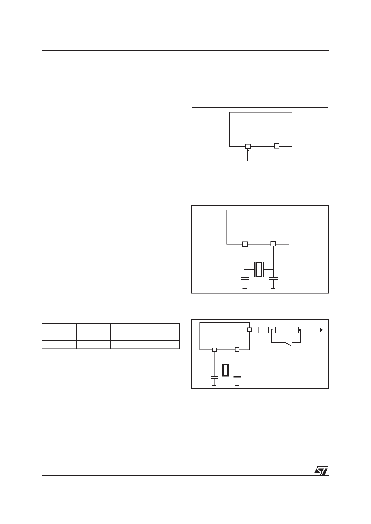
The internal oscillator is designed to operate with
an AT-cut parallel resonant quartz crystal resona-
tor in the frequency range specified for f
osc
.The
circuit shown in Figure 11 is recommended when
using a crystal, and Table 5 lists the recommend-
ed capacitance and feedback resistance values.
The crystal and associated componentsshould be
mounted as close as possible to the input pins in
order to minimize output distortion and start-up
stabilisation time.
Use of an external CMOS oscillator is recom-
mended when crystals outside the specified fre-
quency ranges are to be used.
3.1.2 External Clock
An externalclock maybe applied tothe OSCIN in-
put with the OSCOUT pin not connected, as
shown onFigure 10.
Table 5 Recommended Values for 16 MHz
Crystal Resonator (C
0
< 7pF)
R
SMAX
: Parasitic series resistance of the quartz
crystal (upperlimit).
C
0
: Parasitic shunt capacitance of the quartz crys-
tal (upper limit 7pF).
C
OSCOUT
,C
OSCIN
: Maximum total capacitance on
pins OSCIN and OSCOUT (the valueincludes the
external capacitance tied to the pin plus the para-
sitic capacitance of the board and of the device).
Figure 10. External Clock Source Connections
Figure 11. Crystal/CeramicResonator
Figure 12. Clock Prescaler Block Diagram
R
SMAX
40 Ω 60 Ω 150 Ω
C
OSCIN
56pF 47pF 22pF
C
OSCOUT
56pF 47pF 22pF
OSCIN OSCOUT
EXTERNAL
CLOCK
NC
OSCIN OSCOUT
C
OSCIN
C
OSCOUT
OSCIN
OSCOUT
C
OSCIN C
OSCOUT
%2 %2,4,8, 16
f
CPU
to CPU and
Peripherals
18
19/106
ST72E331 ST72T331
3.2 RESET
3.2.1 Introduction
There are four sources of Reset:
– RESET pin (externalsource)
– Power-On Reset (Internal source)
– WATCHDOG (Internal Source)
– Low Voltage Detection Reset (internal source)
The Reset Service Routine vectoris located at ad-
dress FFFEh-FFFFh.
3.2.2 External Reset
The RESET pin is both an input and an open-drain
output with integrated pull-up resistor. When one
of the internal Reset sources is active, the Reset
pin is driven low for a duration of t
RESET
to reset
the whole application.
3.2.3 ResetOperation
The duration of the Reset state is a minimum of
4096 internal CPU Clock cycles. During the Reset
state, all I/Os take their reset value.
A Reset signal originating from an externalsource
must have a duration of at least t
PULSE
in orderto
be recognised. This detection is asynchronous
and therefore the MCUcan enter Reset state even
in Halt mode.
At the end of the Reset cycle, the MCU may be
held in the Reset state by an External Reset sig-
nal. The RESET pin may thus be used to ensure
V
DD
has risen toa point where the MCU can oper-
ate correctly before the user program is run. Fol-
lowing a Reset event, or after exiting Halt mode, a
4096 CPU Clock cycle delay period is initiated in
order to allow the oscillator to stabilise and to en-
sure that recovery has taken place from theReset
state.
In the high state, the RESET pin is connected in-
ternally to a pull-up resistor (R
ON
). This resistor
can be pulled low by external circuitry to reset the
device.
The RESET pin is an asynchronous signal which
plays a majorrole inEMS performance. In a noisy
environment, it is recommended to use the exter-
nal connections shown in Figure 6.
Figure 13. Reset Block Diagram
INTERNAL
RESET
WATCHDOG RESET
OSCILLATOR
SIGNAL
COUNTER
RESET
TO ST7
RESET
POWER-ON RESET
V
DD
LOW VOLTAGE DETECTOR RESET
R
ON
19
20/106
ST72E331 ST72T331
RESET (Cont’d)
3.2.4 LowVoltage Detector Reset
The on-chip Low Voltage Detector (LVD) gener-
ates a static reset when the supply voltage is be-
low a reference value. The LVD functions both
during power-on as well as when the power supply
drops (brown-out). The reference value for a volt-
age drop islower than the referencevalue for pow-
er-on in order to avoid a parasitic reset when the
MCU starts running and sinks current on the sup-
ply (hysteresis).
The LVD Reset circuitry generates a reset when
V
DD
is below:
V
LVDUP
when V
DD
is rising
V
LVDDOWN
when V
DD
is falling
Provided the minimun V
DD
value (guaranteed for
the oscillator frequency) is above V
LVDDOWN
, the
MCU can only be in two modes:
- underfull softwarecontrol or
- instatic safe reset
In this condition, secure operation is always en-
sured for the application without the need for ex-
ternal reset hardware.
During a Low Voltage Detector Reset, the RESET
pin is held low, thus permitting the MCU to reset
other devices.
In noisy environments, the power supplymay drop
for short periods and cause the Low Voltage De-
tector to generate a Reset too frequently. In such
cases, it is recommended to use devices without
the LVD Reset option and to rely on the watchdog
function to detect application runaway conditions.
Figure14.LowVoltage Detector ResetFunction
Figure 15. Low Voltage Detector Reset Signal
Note: See electrical characteristics for values of
V
LVDUP
and V
LVDDOWN
Figure 16. Temporization timing diagram after an internal Reset
LOW VOLTAGE
DETECTOR RESET
V
DD
FROM
WATCHDOG
RESET
RESET
RESET
V
DD
V
LVDUP
V
LVDDOWN
V
DD
Addresses
$FFFE
Temporization (4096CPU clock cycles)
V
LVDUP
20

21/106
ST72E331 ST72T331
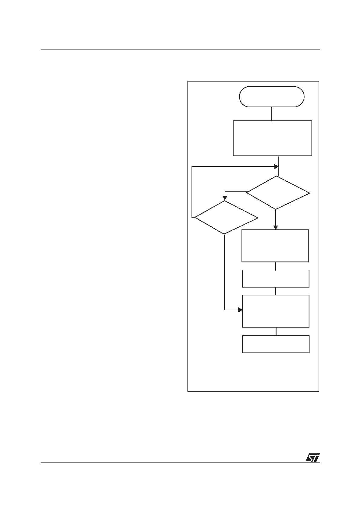
3.3 INTERRUPTS
The ST7 coremay be interrupted by one of two dif-
ferent methods: maskable hardware interrupts as
listed in the Interrupt Mapping Table and a non-
maskable software interrupt (TRAP). The Interrupt
processing flowchartis shown in Figure 17.
The maskable interrupts mustbe enabled clearing
the I bitin order tobe serviced. However, disabled
interrupts may be latched and processed when
they are enabled (see external interrupts subsec-
tion).
When an interrupt has to be serviced:
– Normal processing is suspended at the end of
the current instruction execution.
– The PC, X, A and CC registersare saved onto
the stack.
– The I bit of theCC register isset to prevent addi-
tional interrupts.
– ThePC is thenloaded with the interrupt vectorof
the interrupt to service and the first instructionof
the interrupt serviceroutine is fetched (refer to
the Interrupt Mapping Table for vector address-
es).
The interrupt service routine should finish with the
IRET instruction which causes the contents of the
saved registersto be recovered from thestack.
Note: As a consequence of the IRET instruction,
the I bit will be cleared and the main program will
resume.
Priority management
By default, a servicing interrupt can not be inter-
rupted because the I bit is set by hardware enter-
ing in interrupt routine.
In the case several interrupts are simultaneously
pending, an hardware priority defines which one
will be serviced first (seethe Interrupt Mapping Ta-
ble).
Non Maskable Software Interrupts
This interrupt is entered when the TRAP instruc-
tion is executed regardless of the state of theI bit.
It will be serviced according to the flowchart on
Figure 17.
Interrupts and Low power mode
All interrupts allowthe processor to leave the Wait
low power mode. Only external and specific men-
tioned interrupts allow the processor to leave the
Halt low power mode (refer to the “Exit from HALT“
column in the Interrupt Mapping Table).
External Interrupts
External interrupt vectorscan be loaded in the PC
register if the corresponding external interrupt oc-
curred and if the I bit is cleared. These interrupts
allow the processor to leave the Halt low power
mode.
The external interrupt polarity is selected through
the miscellaneous register or interrupt register (if
available).
External interrupt triggered on edge will be latched
and the interrupt request automatically cleared
upon entering the interrupt service routine.
If several input pins, connected to the same inter-
rupt vector, are configured as interrupts, their sig-
nals are logically ANDed before entering the edge/
level detection block.
Warning: The type of sensitivity defined in the
Miscellaneous or Interrupt register (if available)
applies to the EI source. In case of an ANDed
source (as described on the I/O ports section), a
low level on an I/O pin configured as input with in-
terrupt, masks the interrupt request even in case
of rising-edge sensitivity.
Peripheral Interrupts
Different peripheral interrupt flags in the status
register are able to cause an interrupt when they
are active if both:
– TheI bit of the CC register is cleared.
– Thecorresponding enable bit is setin the control
register.
If any of these two conditions is false, the interrupt
is latched and thus remains pending.
Clearing an interrupt request is done by:
– writing “0” to the corresponding bit in the status
register or
– anaccess to the status register while the flag is
set followed bya read or write of an associated
register.
Note: the clearing sequence resets the internal
latch. A pending interrupt (i.e. waiting for being en-
abled) will therefore be lost if the clear sequence is
executed.
21
22/106
ST72E331 ST72T331
INTERRUPTS (Cont’d)
Figure 17. Interrupt Processing Flowchart
BIT I SET
Y
N
IRET
Y
N
FROM RESET
LOAD PC FROM INTERRUPT VECTOR
STACK PC, X, A, CC
SET I BIT
FETCH NEXT INSTRUCTION
EXECUTE INSTRUCTION
THIS CLEARS I BIT BY DEFAULT
RESTORE PC,X, A, CC FROM STACK
BIT I SET
Y
N
22
23/106
ST72E331 ST72T331
Table 6. Interrupt Mapping
Source
Block
Description
Register
Label
Flag
Exit
from
HALT
Vector
Address
Priority
Order
RESET Reset N/A N/A yes FFFEh-FFFFh
TRAP Software N/A N/A no FFFCh-FFFDh
NOT USED FFFAh-FFFBh
NOT USED FFF8h-FFF9h
EI0 Ext. Interrupt (Ports PA0:PA3) N/A N/A
yes
FFF6h-FFF7h
EI1 Ext. Interrupt (Ports PF0:PF2) N/A N/A FFF4h-FFF5h
EI2 Ext. Interrupt (Ports PB0:PB3) N/A N/A FFF2h-FFF3h
EI3 Ext. Interrupt (Ports PB4:PB7) N/A N/A FFF0h-FFF1h
NOT USED FFEEh-FFEFh
SPI
Transfer Complete
SPISR
SPIF
no
FFECh-FFEDh
Mode Fault MODF
TIMER A
Input Capture 1
TASR
ICF1_A
FFEAh-FFEBh
Output Compare 1 OCF1_A
Input Capture 2 ICF2_A
Output Compare 2 OCF2_A
Timer Overflow TOF_A
TIMER B
Input Capture 1
TBSR
ICF1_B
FFE8h-FFE9h
Output Compare 1 OCF1_B
Input Capture 2 ICF2_B
Output Compare 2 OCF2_B
Timer Overflow TOF_B
SCI
Transmit Buffer Empty
SCISR
TDRE
FFE6h-FFE7h
Transmit Complete TC
Receive Buffer Full RDRF
Idle Line Detect IDLE
Overrun OR
EEPROM EEPROM End of Programming EEPCR E2ITE FFE4h-FFE5h
NOT USED FFE2h-FFE3h
NOT USED FFE0h-FFE1h
Highest
Priority
Priority
Lowest
23
24/106
ST72E331 ST72T331
3.4 POWER SAVING MODES
3.4.1 Introduction
There are threePower Savingmodes. Slow Mode
is selected by setting the relevant bits in the Mis-
cellaneous register. Wait and Halt modes may be
entered usingthe WFI and HALT instructions.
3.4.2 Slow Mode
In Slow mode, the oscillator frequency can be di-
vided by a value defined in the Miscellaneous
Register. The CPU and peripherals are clocked at
this lower frequency. Slow mode isused to reduce
power consumption, andenables the userto adapt
clock frequencyto available supply voltage.
3.4.3 Wait Mode
Wait mode places the MCU in a low power con-
sumption mode by stoppingthe CPU. Allperipher-
als remain active. During Wait mode, the I bit (CC
Register) is cleared, so as to enable all interrupts.
All otherregisters and memory remain unchanged.
The MCU will remain in Wait mode until an Inter-
rupt or Reset occurs, whereupon the Program
Counter branches to the starting address of the In-
terrupt orReset Service Routine.
The MCU will remain in Waitmode until a Reset or
an Interrupt occurs, causing it to wake up.
Refer to Figure 18 below.
Figure 18. WAIT Flow Chart
WFI INSTRUCTION
RESET
INTERRUPT
Y
N
N
Y
CPU CLOCK
OSCILLATOR
PERIPH. CLOCK
I-BIT
ON
ON
CLEARED
OFF
Note: Before servicing an interrupt, the CC register is
pushed on the stack. The I-Bit is set during the inter-
rupt routine and cleared when the CC register is
popped.
4096 CPU CLOCK
FETCH RESET VECTOR
OR SERVICE INTERRUPT
CYCLES DELAY
CPU CLOCK
OSCILLATOR
PERIPH. CLOCK
I-BIT
ON
ON
SET
ON
CPU CLOCK
OSCILLATOR
PERIPH. CLOCK
I-BIT
ON
ON
SET
ON
24
25/106
ST72E331 ST72T331
POWER SAVINGMODES (Cont’d)
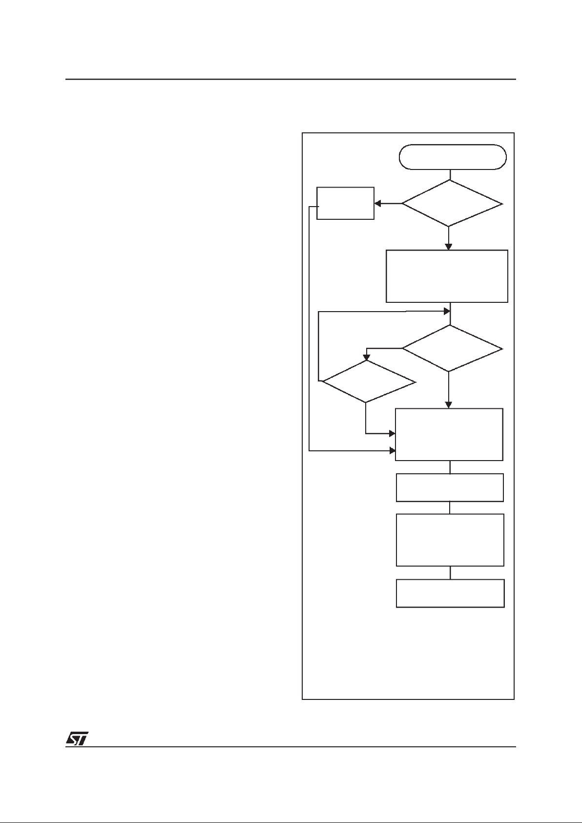
3.4.4 Halt Mode
The Halt mode is the MCU lowest power con-
sumption mode. The Halt mode is entered by exe-
cuting theHALT instruction. The internal oscillator
is then turned off, causing all internal processing to
be stopped, including the operation of the on-chip
peripherals. The Halt mode cannot be used when
the watchdog isenabled, ifthe HALT instruction is
executed while the watchdog system is enabled,a
watchdog reset is generatedthus resetting the en-
tire MCU.
When entering Halt mode, the Ibit in the CC Reg-
ister is clearedso as toenable External Interrupts.
If an interrupt occurs, the CPU becomes active.
The MCU canexit the Halt mode upon reception of
an interrupt or a reset. Refer to the Interrupt Map-
ping Table. The oscillator is then turned on and a
stabilization time is provided beforereleasing CPU
operation. Thestabilization timeis 4096 CPU clock
cycles.
After the start up delay, the CPU continuesoper-
ation byservicing the interrupt whichwakes itup or
by fetching the reset vector if a reset wakes it up.
Figure 19. HALT Flow Chart
N
N
EXTERNAL
INTERRUPT
1)
RESET
HALT INSTRUCTION
4096 CPU CLOCK
FETCH RESET VECTOR
OR SERVICE INTERRUPT
CYCLES DELAY
CPU CLOCK
OSCILLATOR
PERIPH. CLOCK
2)
I-BIT
ON
OFF
SET
ON
CPU CLOCK
OSCILLATOR
PERIPH. CLOCK
I-BIT
OFF
OFF
CLEARED
OFF
Y
Y
WDG
ENABLED?
N
Y
RESET
WATCHDOG
1) or some specific interrupts
Note: Before servicing an interrupt, the CC register is
pushed on the stack. The I-Bit is set during the inter-
rupt routine and cleared when the CC register is
popped.
CPU CLOCK
OSCILLATOR
PERIPH. CLOCK
I-BIT
ON
ON
SET
ON
2) if reset PERIPH. CLOCK = ON ; if interrupt
PERIPH. CLOCK = OFF
25
26/106
ST72E331 ST72T331
3.5 MISCELLANEOUS REGISTER
The Miscellaneous register allows to select the
SLOW operatingmode, the polarity of external in-
terrupt requestsand to output the internal clock.
Register Address:0020h — Read/Write
Reset Value: 0000 0000 (00h)
Bit 7:6 = PEI[3:2]
External Interrupt EI3 and EI2
Polarity Options
.
These bits are set and cleared by software. They
determine which event on EI2 and EI3 causes the
external interrupt according to Table 7.
Table 7. EI2 and EI3 ExternalInterrupt Polarity
Options
Note: Any modification of one of these two bits re-
sets the interrupt request related to this interrupt
vector.
Bit 5 = MCO
Main Clock Out
This bit isset and cleared by software. Whenset, it
enables the output of the Internal Clock on the
PPF0 I/O port.
0 -PF0 is a general purposeI/O port.
1 -MCO alternate function (f
CPU
is output on PF0
pin).
Bit 4:3 = PEI[1:0]
External Interrupt EI1 and EI0
Polarity Options
.
These bits are set and cleared by software. They
determine which event on EI0 and EI1 causes the
external interrupt according to Table 8.
Table 8. EI0 and EI1 External Interrupt Polarity
Options
Note: Any modification of oneof thesetwo bitsre-
sets the interrupt request related to this interrupt
vector.
Bit 2:1 = PSM[1:0]
Prescaler forSlow Mode
These bits are set and cleared by software. They
determine the CPU clock when the SMS bit is set
according to the following table.
Table 9. f
CPU
Value in Slow Mode
Bit 0 = SMS
Slow Mode Select
This bit is set andcleared by software.
0: Normal Mode - f
CPU
=f
OSC
/2
(Reset state)
1: Slow Mode -the f
CPU
valueis determined bythe
PSM[1:0] bits.
70
PEI3 PEI2 MCO PEI1 PEI0 PSM1 PSM0 SMS
MODE PEI3 PEI2
Falling edge and low level
(Reset state)
00
Falling edge only 1 0
Rising edge only 0 1
Rising and falling edge 1 1
MODE PEI1 PEI0
Falling edge and low level
(Reset state)
00
Falling edge only 1 0
Rising edge only 0 1
Rising and falling edge 1 1
f
CPU
Value
PSM1 PSM0
f
OSC
/4 0 0
f
OSC
/16 0 1
f
OSC
/8 1 0
f
OSC
/32 1 1
26

27/106
ST72E331 ST72T331
4 ON-CHIP PERIPHERALS
4.1 I/O PORTS
4.1.1 Introduction
The I/O ports offer different functional modes:
– transferof datathrough digital inputs and outputs
and forspecific pins:
– analog signal input (ADC)
– alternate signal input/output for the on-chip pe-
ripherals.
– external interrupt generation
An I/O port is composed of up to 8 pins. Each pin
can be programmedindependently as digital input
(with or without interrupt generation) or digital out-
put.
4.1.2 Functional Description
Each portis associated to 2 main registers:
– Data Register (DR)
– Data Direction Register (DDR)
and someof them to an optional register:
– Option Register(OR)
Each I/Opin may beprogrammed using thecorre-
sponding register bits in DDR and OR registers: bit
X corresponding to pin X of the port. The same cor-
respondence is used for the DR register.
The following description takes into account the
OR register, for specific ports whichdo not provide
this register refer to the I/O Port Implementation
Section 4.1.3. The generic I/O block diagram is
shown onFigure 21.
4.1.2.1 Input Modes
The input configuration isselected by clearing the
corresponding DDRregister bit.
In this case, reading the DR register returns the
digital value applied to the external I/O pin.
Different input modes can be selected by software
through theOR register.
Notes:
1. All the inputs are triggered by a Schmitt trigger.
2. When switching from input mode to output
mode, the DR register should be written first to
output the correct value as soon as the port is con-
figured as an output.
Interrupt function
When an I/O is configured in Input with Interrupt,
an event on this I/O can generate an external In-
terrupt request to the CPU. The interrupt polarity is
given independently according to the description
mentioned in the Miscellaneous register or in the
interrupt register (where available).
Each pin can independently generate an Interrupt
request.
Each external interrupt vector is linked to a dedi-
cated group of I/O port pins (see Interrupts sec-
tion). If several input pins are configured as inputs
to the same interrupt vector, their signals are logi-
cally ANDed before entering the edge/level detec-
tion block. For this reason if one of the interrupt
pins is tied low, it masks the other ones.
4.1.2.2 Output Mode
The pin is configured in output modeby setting the
corresponding DDR registerbit.
In this mode, writing “0” or “1” to the DR register
applies this digital value to the I/O pin through the
latch. Then reading the DR register returns the
previously stored value.
Note: In this mode, the interrupt function is disa-
bled.
4.1.2.3 Digital Alternate Function
When an on-chipperipheral is configured to use a
pin, the alternate function is automatically select-
ed. This alternate function takes priority over
standard I/O programming. When the signal is
coming from an on-chip peripheral, the I/O pin is
automatically configuredin output mode (push-pull
or open drain according to the peripheral).
When the signal is going to an on-chip peripheral,
the I/O pin has to be configured ininput mode. In
this case, the pin’s state is also digitally readable
by addressing the DR register.
Notes:
1. Input pull-up configuration can cause an unex-
pected value atthe input of the alternate peripher-
al input.
2. When the on-chip peripheral uses apin asinput
and output, this pin must be configured asan input
(DDR = 0).
Warning
: The alternate function must not be acti-
vated as long as the pin isconfigured as input with
interrupt, in order to avoid generating spurious in-
terrupts.
27
28/106
ST72E331 ST72T331
I/O PORTS (Cont’d)
4.1.2.4 Analog Alternate Function
When the pin isused asan ADC input theI/O must
be configured as input, floating. The analog multi-
plexer (controlled by the ADC registers) switches
the analog voltage present on the selected pin to
the common analog rail which is connected to the
ADC input.
It isrecommended not to change the voltage level
or loading on any port pin while conversion is in
progress. Furthermore it is recommended not to
have clocking pins located close to a selected an-
alog pin.
Warning
: The analog input voltage level must be
within the limits stated in the Absolute Maximum
Ratings.
4.1.3 I/O Port Implementation
The hardware implementation oneach I/O port de-
pends on the settingsin the DDR andOR registers
and specific feature of the I/O portsuch as ADCIn-
put (see Figure 21) or true open drain. Switching
these I/O ports from one state to another should
be done in a sequence that prevents unwanted
side effects. Recommended safetransitions are il-
lustrated in Figure 20. Other transitions are poten-
tially risky and should be avoided, since they are
likely to present unwanted side-effects such as
spurious interrupt generation.
Figure 20. Recommended I/O State Transition Diagram
with interrupt
INPUT
OUTPUT
no interrupt
INPUT
push-pullopen-drain
OUTPUT
28
29/106
ST72E331 ST72T331
I/O PORTS (Cont’d)
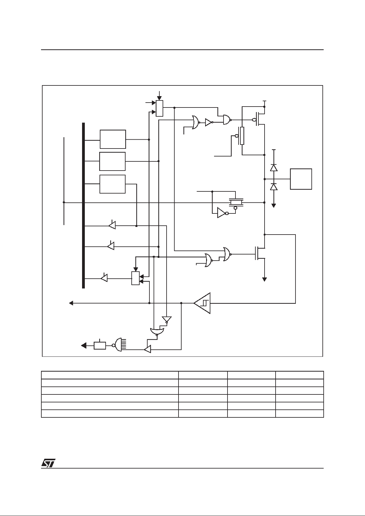
Figure 21. I/O BlockDiagram
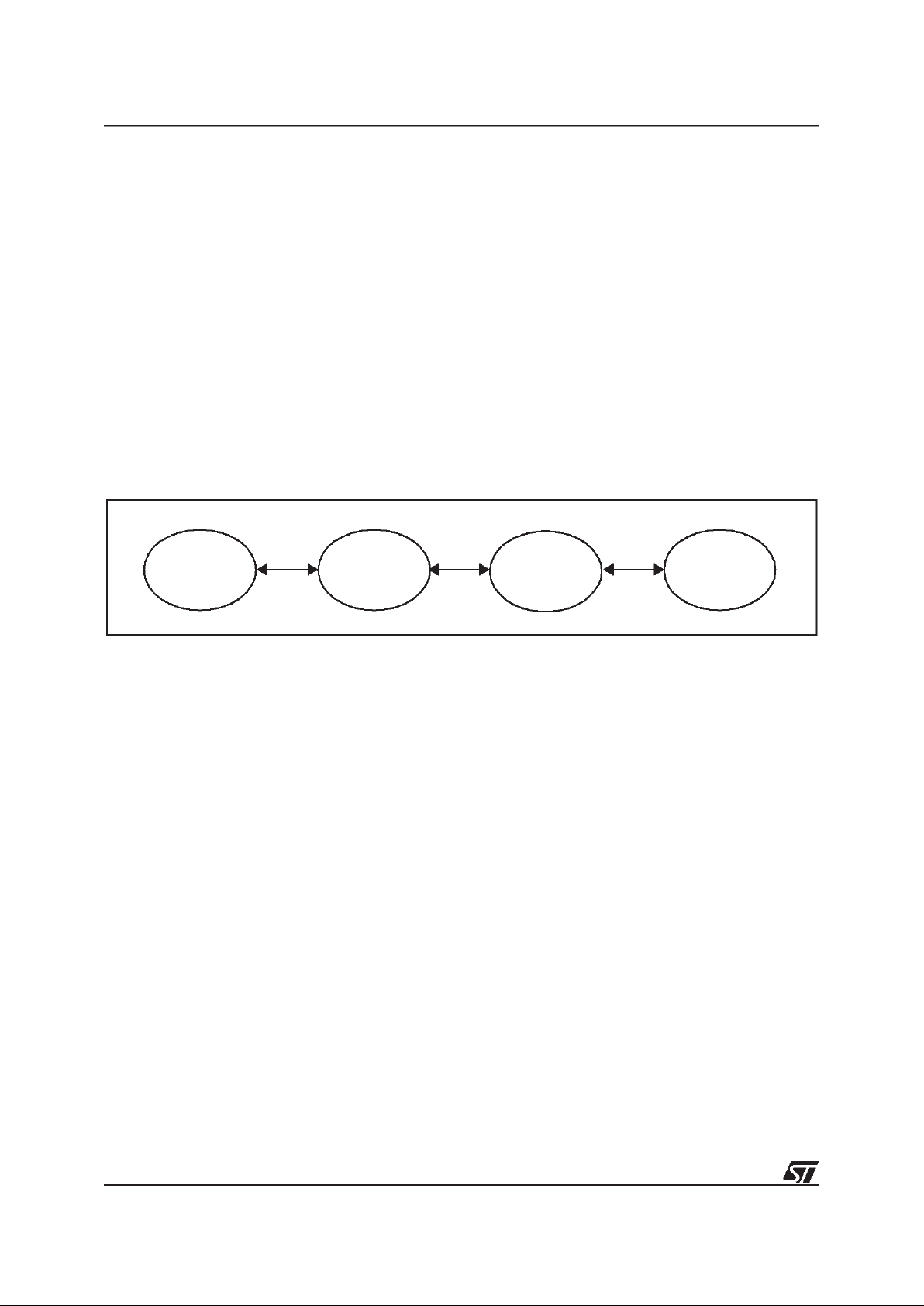
Table 10. Port Mode Configuration
Legend:
0 - present, not activated
1 - present and activated
Notes:
– No OR Register on some ports (see register map).
– ADC Switch on ports with analog alternate functions.
DR
DDR
LATCH
LATCH
DATA BUS
DR SEL
DDR SEL
V
DD
PAD
ANALOG
SWITCH
ANALOG ENABLE
(ADC)
M
U
X
ALTERNATE
ALTERNATE
ALTERNATE ENABLE
COMMON ANALOG RAIL
ALTERNATE
M
U
X
ALTERNATE INPUT
PULL-UP
OUTPUT
P-BUFFER
(S
EE TABLE BELOW)
N-BUFFER
1
0
1
0
OR
LATCH
ORSEL
FROM
OTHER
BITS
EXTERNAL
PULL-UP
CONDITION
ENABLE
ENABLE
GND
(S
EE TABLE BELOW)
(S
EE NOTE BELOW)
CMOS
SCHMITT TRIGGER
SOURCE (EIx)
INTERRUPT
POLARITY
SEL
GND
V
DD
DIODE
(SEE TABLEBELOW)
Configuration Mode Pull-up P-buffer V
DD
Diode
Floating 0 0 1
Pull-up 1 0 1
Push-pull 0 1 1
True Open Drain not present not present not present
Open Drain (logic level) 0 0 1
29

30/106
ST72E331 ST72T331
I/O PORTS (Cont’d)
Table 11. Port Configuration
Notes:
1. ST72T331N only
2. For OTP/EPROM version, when OR=0: floating & when OR=1: reserved
3. For OTP/EPROM version, when OR=0: open-drain, high sink capability & when OR=1: reserved
* Reset state (The bits corresponding to unavailable pins are forced to 1 by hardware, this affects thereset status value).
Warning: All bits of the DDR register which correspond to unconnected I/Os must be left at their reset value. They must
not be modified by the user otherwise a spurious interrupt may be generated.
Port Pin name
Input (DDR = 0) Output (DDR = 1)
OR= 0 OR= 1 OR = 0 OR =1
Port A
PA0:PA2
1)
floating* pull-up with interrupt open-drain push-pull
PA3 floating* pull-up with interrupt open-drain push-pull
PA4:PA7 floating* open drain, high sink capability
Port B
PB0:PB4 floating* pull-up with interrupt open-drain
push-pull
PB5:PB7
1)
floating* pull-up with interrupt open-drain
push-pull
Port C PC0:PC7 floating* pull-up open-drain push-pull
Port D
PD0:PD5 floating* pull-up open-drain push-pull
PD6:PD7
1)
floating* pull-up open-drain push-pull
Port E
PE0:PE1 floating* pull-up open-drain push-pull
PE4:PE7
1)
floating*
2)
open drain, high sink capability
3)
Port F
PF0:PF2 floating* pull-up with interrupt open-drain push-pull
PF4, PF6,PF7 floating* pull-up open-drain push-pull
30
 Loading...