


SGS Thomson Microelectronics ST3232ECWR, ST3232ECTR, ST3232ECN, ST3232ECDR, ST3232ECD Datasheet
...ST3232E
±15KV ESD-PROTECTED, 3 TO 5.5V, LOW POWER, UP TO 250KBPS, RS-232 DRIVERS AND RECEIVERS
■ESD PROTECTIO FOR RS-232 I/O PINS ±15KV HUMAN BODY MODEL
±8KV IEC 1000-4-2 CONTACT DISCHARGE
■300μA SUPPLY CURRENT
■250Kbps MINIMUM GUARENTEED DATA RATE
■6V/μs MINIMUM GUARANTEED SLEW RATE
■MEET EIA/TIA-232 SPECIFICATIONS DOWN TO 3V
■AVAILABLE IN DIP-16, SO-16, SO-16 LARGE SSOP16 AND TSSOP16
DESCRIPTION
The ST3232E is a 3V powered EIA/TIA-232 and V.28/V.24 communication interfaces with low power requirements, high data-rate capabilities and enhanced electrostatic discharge (ESD) protection to ±8kV using IEC1000-4-2 Contact Discharge and ±15kV using the Human Body Model. ST3232E has a proprietary low dropout transmitter output stage providing true RS-232 performance from 3 to 5V supplies witha a dual charge pump. The charge pump requires only four small 0.1μF standard external capacitors for operations from 3V supply.
The ST3232E has two receivers and two drivers.
DIP |
|
SOP |
SOP Large |
SSOP |
TSSOP |
The device is guaranteed to run at data rates of 250Kbps while maintaining RS-232 output levels. Typical applications are Notebook, Subnotebook and Palmtop Computers, Battery Powered Equipment, Hand-Held Equipment, Peripherals and Printers.
ORDERING CODES
Type |
Temperature |
Package |
Comments |
|
Range |
||||
|
|
|
||
|
|
|
|
|
ST3232ECN |
0 to 70 °C |
DIP-16 |
25parts per tube / 40tube per box |
|
|
|
|
|
|
ST3232EBN |
-40 to 85 °C |
DIP-16 |
25parts per tube / 40tube per box |
|
|
|
|
|
|
ST3232ECD |
0 to 70 °C |
SO-16 (Tube) |
50parts per tube / 20tube per box |
|
|
|
|
|
|
ST3232EBD |
-40 to 85 °C |
SO-16 (Tube) |
50parts per tube / 20tube per box |
|
|
|
|
|
|
ST3232ECDR |
0 to 70 °C |
SO-16 (Tape & Reel) |
2500 parts per reel |
|
|
|
|
|
|
ST3232EBDR |
-40 to 85 °C |
SO-16 (Tape & Reel) |
2500 parts per reel |
|
|
|
|
|
|
ST3232ECW |
0 to 70 °C |
SO-16 Large (Tube) |
50parts per tube / 20tube per box |
|
|
|
|
|
|
ST3232EBW |
-40 to 85 °C |
SO-16 Large (Tube) |
50parts per tube / 20tube per box |
|
ST3232ECWR |
0 to 70 °C |
SO-16 Large (Tape & Reel) |
1000 parts per reel |
|
|
|
|
|
|
ST3232EBWR |
-40 to 85 °C |
SO-16 Large (Tape & Reel) |
1000 parts per reel |
|
|
|
|
|
|
ST3232ECPR |
0 to 70 °C |
SSOP16 (Tape & Reel) |
1350 parts per reel |
|
|
|
|
|
|
ST3232EBPR |
-40 to 85 °C |
SSOP16 (Tape & Reel) |
1350 parts per reel |
|
|
|
|
|
|
ST3232ECTR |
0 to 70 °C |
TSSOP16 (Tape & Reel) |
2500 parts per reel |
|
|
|
|
|
|
ST3232EBTR |
-40 to 85 °C |
TSSOP16 (Tape & Reel) |
2500 parts per reel |
|
|
|
|
|
|
April 2003 |
|
|
1/16 |
|
|
|
|
|
ST3232E
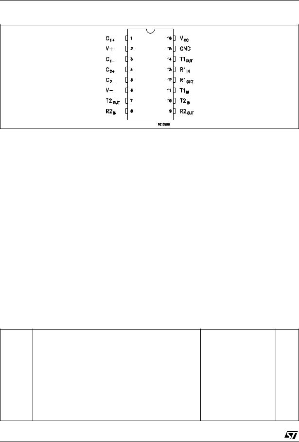
PIN CONFIGURATION
PIN DESCRIPTION
PlN N° |
SYMBOL |
NAME AND FUNCTION |
|
|
|
1 |
C1+ |
Positive Terminal for the first Charge Pump Capacitor |
2 |
V+ |
Doubled Voltage Terminal |
|
|
|
3 |
C1- |
Negative Terminal for the first Charge Pump Capacitor |
4 |
C2+ |
Positive Terminal for the second Charge Pump Capacitor |
5 |
C2- |
Negative Terminal for the second Charge Pump Capacitor |
6 |
V- |
Inverted Voltage Terminal |
7 |
T2OUT |
Second Transmitter Output Voltage |
8 |
R2IN |
Second Receiver Input Voltage |
9 |
R2OUT |
Second Receiver Output Voltage |
10 |
T2IN |
Second Transmitter Input Voltage |
11 |
T1IN |
First Transmitter Input Voltage |
12 |
R1OUT |
First Receiver Output Voltage |
13 |
R1IN |
First Receiver Input Voltage |
14 |
T1OUT |
First Transmitter Output Voltage |
15 |
GND |
Ground |
|
|
|
16 |
VCC |
Supply Voltage |
ABSOLUTE MAXIMUM RATINGS
Symbol |
Parameter |
Value |
Unit |
|
|
|
|
VCC |
Supply Voltage |
-0.3 to 6 |
V |
V+ |
Doubled Voltage Terminal |
(VCC - 0.3) to 7 |
V |
V- |
Inverted Voltage Terminal |
0.3 to -7 |
V |
|
|
|
|
V+ +|V-| |
|
13 |
V |
|
|
|
|
TIN |
Transmitter Input Voltage Range |
-0.3 to 6 |
V |
RIN |
Receiver Input Voltage Range |
± 25 |
V |
TOUT |
Transmitter Output Voltage Range |
± 13.2 |
V |
ROUT |
Receiver Output Voltage Range |
-0.3 to (VCC + 0.3) |
V |
tSHORT |
Transmitter Output Short to GND Time |
Continuous |
|
Absolute Maximum Ratings are those values beyond which damage to the device may occur. Functional operation under these condition is not implied. V+ and V- can have a maximum magnitude of +7V, but their absolute addition can not exceed 13 V.
2/16

|
|
|
|
|
|
ST3232E |
|
ESD PERFORMANCE: TRANSMITTER OUTPUTS, RECEIVER INPUTS |
|
|
|
|
|||
|
|
|
|
|
|
|
|
Symbol |
Parameter |
Test Conditions |
|
Min. |
Typ. |
Max. |
Unit |
|
|
|
|
|
|
|
|
ESD |
ESD Protection Voltage |
Human Body Model |
|
±15 |
|
|
kV |
|
|
|
|
|
|
|
|
ESD |
ESD Protection Voltage |
IEC-1000-4-2 |
|
±8 |
|
|
kV |
ELECTRICAL CHARACTERISTICS
(C1 - C4 = 0.1μF, VCC = 3V to 5.5V, TA = -40 to 85°C, unless otherwise specified. Typical values are referred to TA = 25°C)
Symbol |
Parameter |
|
Test Conditions |
Min. |
Typ. |
Max. |
Unit |
|
|
|
|
|
|
|
|
ISUPPLY |
VCC Power Supply Current |
No Load |
VCC = 3V or 5V TA = 25°C |
|
0.3 |
1 |
mA |
LOGIC INPUT ELECTRICAL CHARACTERISTICS
(C1 - C4 = 0.1μF, VCC = 3V to 5.5V, TA = -40 to 85°C, unless otherwise specified. Typical values are referred to TA = 25°C)
Symbol |
Parameter |
Test Conditions |
Min. |
Typ. |
Max. |
Unit |
|
|
|
|
|
|
|
VTIL |
Input Logic Threshold Low |
T-IN |
|
|
0.8 |
V |
VHYS |
Transmitter Input |
|
|
0.25 |
|
V |
|
Histeresys |
|
|
|
|
|
VTIH |
Input Logic Threshold High |
VCC = 3.3V |
2 |
|
|
V |
|
|
VCC = 5V |
2.4 |
|
|
|
IIL |
Input Leakage Current |
T-IN |
|
± 0.01 |
± 1 |
μA |
TRANSMITTER ELECTRICAL CHARACTERISTICS
(C1 - C4 = 0.1μF tested at VCC = 3V to 5.5V, TA = -40 to 85°C, unless otherwise specified. Typical values are referred to TA = 25°C)
Symbol |
Parameter |
Test Conditions |
Min. |
Typ. |
Max. |
Unit |
|
|
|
|
|
|
|
|
|
VTOUT |
Output Voltage Swing |
All Transmitter outputs are loaded with |
± 5 |
± 5.4 |
|
V |
|
|
|
3KΩ to GND |
|
|
|
|
|
RTOUT |
Transmitter Output |
VCC = V+ = V- = 0V |
VOUT = ± 2V |
300 |
10M |
|
Ω |
|
Resistance |
|
|
|
|
|
|
ITSC |
Output Short Circuit |
|
|
|
± 60 |
|
mA |
|
Current |
|
|
|
|
|
|
ITOL |
Output Leakage Current |
VCC = 0V or 3V to 5.5V |
VOUT = ± 12V |
|
|
± 25 |
μA |
|
|
Transmitters Disable |
|
|
|
|
|
|
|
|
|
|
|
|
|
3/16

ST3232E
RECEIVER ELECTRICAL CHARACTERISTICS
(C1 - C4 = 0.1μF tested at VCC = 3V to 5.5V, TA = -40 to 85°C, unless otherwise specified. Typical values are referred to TA = 25°C)
Symbol |
Parameter |
|
Test Conditions |
Min. |
Typ. |
Max. |
Unit |
|
|
|
|
|
|
|
|
VRIN |
Receiver Input Voltage |
|
|
-25 |
|
25 |
V |
|
Operating Range |
|
|
|
|
|
|
VRIL |
RS-232 Input Threshold |
TA = 25°C |
V CC = 3.3V |
0.6 |
1.1 |
|
V |
|
Low |
|
|
|
|
|
|
|
TA = 25°C |
V CC = 5V |
0.8 |
1.5 |
|
|
|
|
|
|
|
||||
VRIH |
RS-232 Input Threshold |
TA = 25°C |
V CC = 3.3V |
|
1.4 |
2.4 |
V |
|
High |
|
|
|
|
|
|
|
TA = 25°C |
V CC = 5V |
|
1.8 |
2.4 |
|
|
|
|
|
|
||||
VRIHYS |
Input Hysteresis |
|
|
|
0.5 |
|
V |
RRIN |
Input Resistance |
TA = 25°C |
|
3 |
5 |
7 |
K Ω |
VROL |
TTL/CMOS Output Voltage |
IOUT = 1.6mA |
|
|
0.4 |
V |
|
|
Low |
|
|
|
|
|
|
VROH |
TTL/CMOS Output Voltage |
IOUT = -1mA |
VCC-0.6 |
VCC-0.1 |
|
V |
|
|
High |
|
|
|
|
|
|
TIMING CHARACTERISTICS
(C1 - C4 = 0.1μF, VCC = 3V to 5.5V, TA = -40 to 85°C, unless otherwise specified. Typical values are referred to TA = 25°C)
Symbol |
Parameter |
|
Test Conditions |
Min. |
Typ. |
Max. |
Unit |
|
|
|
|
|
|
|
|
|
|
DR |
Data Transfer Rate |
RL = 3KΩ |
CL2= 1000pF |
250 |
|
|
Kbps |
|
|
|
one trasmitter switching |
|
|
|
|
||
tPHLR |
Propagation Delay Input to |
RXIN = RXOUT |
CL = 150pF |
|
0.15 |
|
μs |
|
tPLHR |
Output |
|
|
|
|
|
|
|
tOER |
Receiver Output Enable |
Normal Operation |
|
|
50 |
|
ns |
|
|
Time |
|
|
|
|
|
|
|
tODR |
Receiver Output Disable |
Normal Operation |
|
|
50 |
|
ns |
|
|
Time |
|
|
|
|
|
|
|
|tPHLT |
Transmitter Propagation |
(Note 1) |
|
|
|
200 |
|
ns |
- tTHL| |
Delay Difference |
|
|
|
|
|
|
|
|tPHLR |
Receiver Propagation Delay |
|
|
|
|
50 |
|
ns |
- tTHR| |
Difference |
|
|
|
|
|
|
|
SRT |
Trnasition Slew Rate |
TA = 25°C |
R L = 3KΩ to 7KΩ VCC = 3.3V |
|
|
|
|
|
|
|
measured from +3V to -3V or -3V to +3V |
6 |
|
30 |
V/μs |
||
|
|
CL = 150pF to 1000pF |
|
|||||
|
|
CL = 150pF to 2500pF |
4 |
|
30 |
V/μs |
||
|
|
|
|
|
|
|||
Transmitter Skew is measured at the transmitter zero cross points |
|
|
|
|
|
|||
4/16

ST3232E
APPLICATION CIRCUITS
CAPACITANCE VALUE (μF)
VCC |
C1 |
C2 |
C3 |
C4 |
Cbypass |
3.0 to 3.6 |
0.1 |
0.1 |
0.1 |
0.1 |
0.1 |
|
|
|
|
|
|
4.5 to 5.5 |
0.047 |
0.33 |
0.33 |
0.33 |
0.1 |
|
|
|
|
|
|
3.0 to 5.5 |
0.1 |
0.47 |
0.47 |
0.47 |
0.1 |
5/16
 Loading...