


SGS Thomson Microelectronics ST90E158M9G0, ST90158P9C6, ST90158M9T1, ST90158M9Q6, ST90158M9 Datasheet
...ST90158 - ST90135
8/16-BIT MCU FAMILY WITH UP TO 64K ROM/OTP/EPROM AND UP TO 2K RAM
■Register File based 8/16 bit Core Architecture with RUN, WFI, SLOW and HALT modes
■0 - 16 MHz Operation @ 5V±10%, -40°C to +85°C and 0°C to +70°C Operating Temperature Ranges
■0 - 14 MHz Operation @ 3V±10% and 0°C to +70°C Operating Temperature Range
■Fully Programmable PLL Clock Generator, with Frequency Multiplication and low frequency, low cost external crystal
■Minimum 8-bit Instruction Cycle time: 83ns - (@ 24 MHz internal clock frequency)
■Minimum 16-bit Instruction Cycle time: 250ns - (@ 24 MHz internal clock frequency)
■Internal Memory:
±EPROM/OTP/ROM 16/24/32/48/64K bytes
±ROMless version available
±RAM 512/768/1K/1.5K/2K bytes
■Maximum External Memory: 64K bytes
■224 general purpose registers available as RAM, accumulators or index pointers (register file)
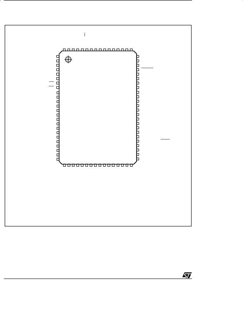
■80-pin Plastic Quad Flat Package and 80-pin Thin Quad Flat Package
■67 fully programmable I/O bits
■8 external and 1 Non-Maskable Interrupts
■DMA Controller and Programmable Interrupt Handler
■Single Master Serial Peripheral Interface
■Two 16-bit Timers with 8-bit Prescaler, one usable as a Watchdog Timer (software and hardware)
■Three (ST90158) or two (ST90135) 16-bit Multifunction Timers, each with an 8 bit prescaler, 12 operating modes and DMA capabilities
■8 channel 8-bit Analog to Digital Converter, with Automatic voltage monitoring capabilities and external reference inputs
■Two (ST90158) or one (ST90135) Serial Communication Interfaces with asynchronous, synchronous and DMA capabilities
■Rich Instruction Set with 14 Addressing modes
■Division-by-Zero trap generation
TQFP80
PQFP80
■Versatile Development Tools, including Assembler, Linker, C-compiler, Archiver, Source Level Debugger and Hardware Emulators with Real-Time Operating System available from Third Parties
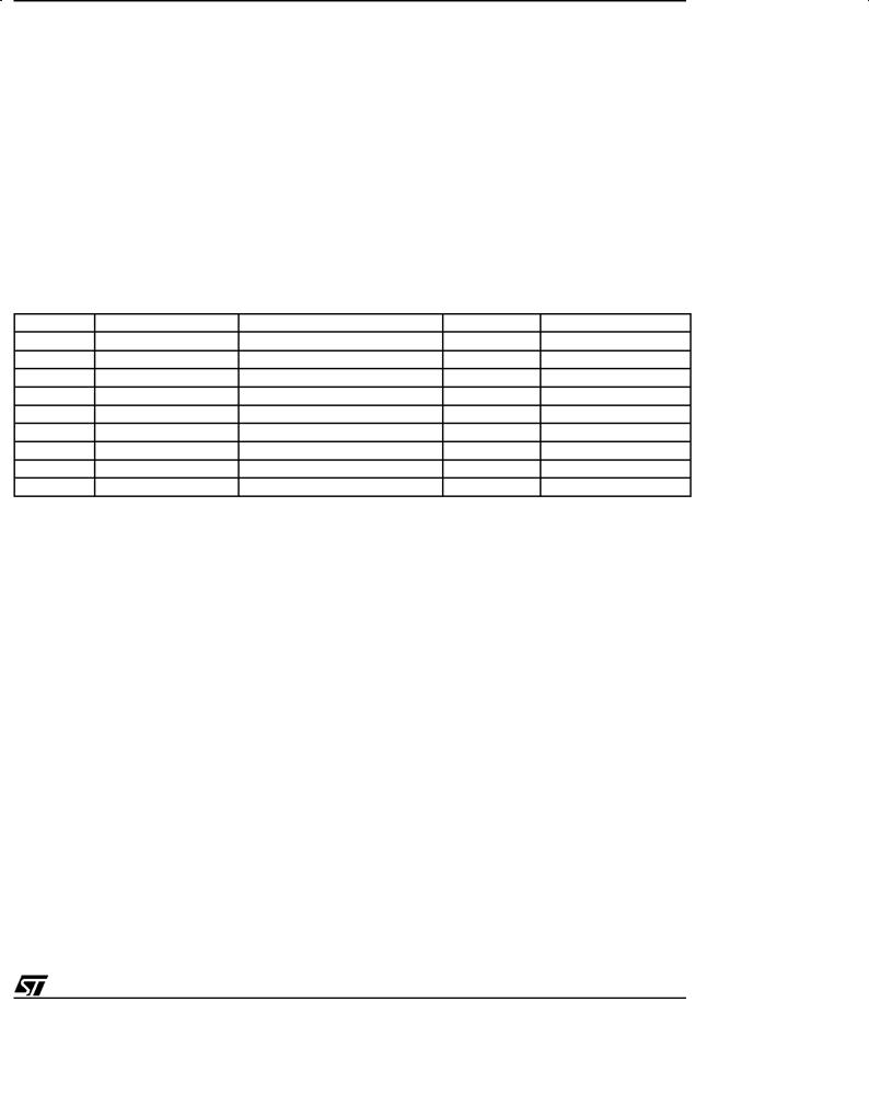
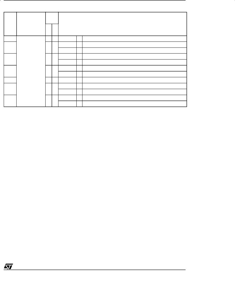
DEVICE SUMMARY
|
Program |
RAM |
|
|
|
|
DEVICE |
Memory |
MFT SCI |
PACKAGE |
|||
(Bytes) |
||||||
|
(Bytes) |
|
|
|
|
|
|
16K ROM |
512 |
2 |
1 |
|
|
ST90135 |
24K ROM |
768 |
2 |
1 |
PQFP80 |
|
|
32K ROM |
1K |
2 |
1 |
||
|
|
|||||
|
48K ROM |
1.5K |
3 |
2 |
|
|
ST90158 |
64k ROM |
2K |
3 |
2 |
PQFP80/ |
|
|
TQFP80 |
|||||
|
|
|
|
|
||
ST90E158 |
64K |
2K |
3 |
2 |
CQFP80 |
|
EPROM |
||||||
|
|
|
|
|
||
ST90E158LV |
64K |
2K |
3 |
2 |
CQFP80 |
|
EPROM |
||||||
|
|
|
|
|
||
ST90T158 |
64K OTP |
2K |
3 |
2 |
PQFP80 |
|
ST90T158LV |
64K OTP |
2K |
3 |
2 |
PQFP80/ |
|
TQFP80/ |
||||||
|
|
|
|
|
||
ST90R158 |
ROMless |
2K |
3 |
2 |
PQFP80/ |
|
TQFP80 |
||||||
|
|
|
|
|
||
Rev. 3.0
January 2000 |
1/190 |

|
|
Table of Contents |
|
1 GENERAL DESCRIPTION . . . . . . . . . . . . . . . . . . . . . . . . . . . . . . . . . . . . . . . . . . . . . . . . . |
. . . . . 6 |
||
1.1 |
INTRODUCTION . . . . . . . . . . . . . . . . . . . . . . . . . . . . . . . . . . . . . . . . . . . . . . . . . . . . |
. . . . . 6 |
|
|
1.1.1 |
ST9+ Core . . . . . . . . . . . . . . . . . . . . . . . . . . . . . . . . . . . . . . . . . . . . . . . . . . . |
. . . . . 6 |
|
1.1.2 |
Power Saving Modes . . . . . . . . . . . . . . . . . . . . . . . . . . . . . . . . . . . . . . . . . . . |
. . . . . 6 |
|
1.1.3 |
system Clock . . . . . . . . . . . . . . . . . . . . . . . . . . . . . . . . . . . . . . . . . . . . . . . . . |
. . . . . 6 |
|
1.1.4 |
I/O Ports . . . . . . . . . . . . . . . . . . . . . . . . . . . . . . . . . . . . . . . . . . . . . . . . . . . . . |
. . . . . 6 |
|
1.1.5 |
Multifunction Timers (MFT) . . . . . . . . . . . . . . . . . . . . . . . . . . . . . . . . . . . . . . . |
. . . . . 7 |
|
1.1.6 |
Standard Timer (STIM) . . . . . . . . . . . . . . . . . . . . . . . . . . . . . . . . . . . . . . . . . . |
. . . . . 7 |
|
1.1.7 |
Watchdog Timer (WDT) . . . . . . . . . . . . . . . . . . . . . . . . . . . . . . . . . . . . . . . . . |
. . . . . 7 |
|
1.1.8 |
Serial Peripheral Interface (SPI) . . . . . . . . . . . . . . . . . . . . . . . . . . . . . . . . . . . |
. . . . . 7 |
|
1.1.9 |
Serial Communications Controllers (SCI) . . . . . . . . . . . . . . . . . . . . . . . . . . . . |
. . . . . 7 |
|
1.1.10 Analog/Digital Converter (ADC) . . . . . . . . . . . . . . . . . . . . . . . . . . . . . . . . . . . |
. . . . . 7 |
|
1.2 |
PIN DESCRIPTION . . . . . . . . . . . . . . . . . . . . . . . . . . . . . . . . . . . . . . . . . . . . . . . . . . |
. . . . 10 |
|
1.3 |
I/O PORT PINS . . . . . . . . . . . . . . . . . . . . . . . . . . . . . . . . . . . . . . . . . . . . . . . . . . . . . |
. . . . 13 |
|
2 DEVICE ARCHITECTURE . . . . . . . . . . . . . . . . . . . . . . . . . . . . . . . . . . . . . . . . . . . . . . . . . |
. . . . 18 |
||
2.1 |
CORE ARCHITECTURE . . . . . . . . . . . . . . . . . . . . . . . . . . . . . . . . . . . . . . . . . . . . . . |
. . . . 18 |
|
2.2 |
MEMORY SPACES . . . . . . . . . . . . . . . . . . . . . . . . . . . . . . . . . . . . . . . . . . . . . . . . . . |
. . . . 18 |
|
|
2.2.1 |
Register File . . . . . . . . . . . . . . . . . . . . . . . . . . . . . . . . . . . . . . . . . . . . . . . . . . |
. . . . 18 |
|
2.2.2 |
Register Addressing . . . . . . . . . . . . . . . . . . . . . . . . . . . . . . . . . . . . . . . . . . . . |
. . . . 20 |
2.3 |
SYSTEM REGISTERS . . . . . . . . . . . . . . . . . . . . . . . . . . . . . . . . . . . . . . . . . . . . . . . . |
. . . . 21 |
|
|
2.3.1 |
Central Interrupt Control Register . . . . . . . . . . . . . . . . . . . . . . . . . . . . . . . . . . |
. . . . 21 |
|
2.3.2 |
Flag Register . . . . . . . . . . . . . . . . . . . . . . . . . . . . . . . . . . . . . . . . . . . . . . . . . |
. . . . 22 |
|
2.3.3 |
Register Pointing Techniques . . . . . . . . . . . . . . . . . . . . . . . . . . . . . . . . . . . . . |
. . . . 23 |
|
2.3.4 |
Paged Registers . . . . . . . . . . . . . . . . . . . . . . . . . . . . . . . . . . . . . . . . . . . . . . . |
. . . . 26 |
|
2.3.5 |
Mode Register . . . . . . . . . . . . . . . . . . . . . . . . . . . . . . . . . . . . . . . . . . . . . . . . |
. . . . 26 |
|
2.3.6 |
Stack Pointers . . . . . . . . . . . . . . . . . . . . . . . . . . . . . . . . . . . . . . . . . . . . . . . . . |
. . . . 27 |
2.4 |
MEMORY ORGANIZATION . . . . . . . . . . . . . . . . . . . . . . . . . . . . . . . . . . . . . . . . . . . . |
. . . . 29 |
|
2.5 |
MEMORY MANAGEMENT UNIT . . . . . . . . . . . . . . . . . . . . . . . . . . . . . . . . . . . . . . . . |
. . . . 30 |
|
2.6 |
ADDRESS SPACE EXTENSION . . . . . . . . . . . . . . . . . . . . . . . . . . . . . . . . . . . . . . . . |
. . . . 31 |
|
|
2.6.1 |
Addressing 16-Kbyte Pages . . . . . . . . . . . . . . . . . . . . . . . . . . . . . . . . . . . . . . |
. . . . 31 |
|
2.6.2 |
Addressing 64-Kbyte Segments . . . . . . . . . . . . . . . . . . . . . . . . . . . . . . . . . . . |
. . . . 32 |
2.7 |
MMU REGISTERS . . . . . . . . . . . . . . . . . . . . . . . . . . . . . . . . . . . . . . . . . . . . . . . . . . . |
. . . . 32 |
|
|
2.7.1 |
DPR[3:0]: Data Page Registers . . . . . . . . . . . . . . . . . . . . . . . . . . . . . . . . . . . |
. . . . 32 |
|
2.7.2 |
CSR: Code Segment Register . . . . . . . . . . . . . . . . . . . . . . . . . . . . . . . . . . . . |
. . . . 34 |
|
2.7.3 ISR: Interrupt Segment Register . . . . . . . . . . . . . . . . . . . . . . . . . . . . . . . . . . . |
. . . . 34 |
|
|
2.7.4 DMASR: DMA Segment Register . . . . . . . . . . . . . . . . . . . . . . . . . . . . . . . . . . |
. . . . 34 |
|
2.8 |
MMU USAGE . . . . . . . . . . . . . . . . . . . . . . . . . . . . . . . . . . . . . . . . . . . . . . . . . . . . . . . |
. . . . 36 |
|
|
2.8.1 |
Normal Program Execution . . . . . . . . . . . . . . . . . . . . . . . . . . . . . . . . . . . . . . . |
. . . . 36 |
|
2.8.2 |
Interrupts . . . . . . . . . . . . . . . . . . . . . . . . . . . . . . . . . . . . . . . . . . . . . . . . . . . . . |
. . . . 36 |
|
2.8.3 |
DMA . . . . . . . . . . . . . . . . . . . . . . . . . . . . . . . . . . . . . . . . . . . . . . . . . . . . . . . . |
. . . . 36 |
3 REGISTER AND MEMORY MAP . . . . . . . . . . . . . . . . . . . . . . . . . . . . . . . . . . . . . . . . . . . . |
. . . . 37 |
||
3.1 |
MEMORY CONFIGURATION . . . . . . . . . . . . . . . . . . . . . . . . . . . . . . . . . . . . . . . . . . |
. . . . 37 |
|
3.2 |
EPROM PROGRAMMING . . . . . . . . . . . . . . . . . . . . . . . . . . . . . . . . . . . . . . . . . . . . . |
. . . . 37 |
|
3.3 |
MEMORY MAP . . . . . . . . . . . . . . . . . . . . . . . . . . . . . . . . . . . . . . . . . . . . . . . . . . . . . |
. . . . 39 |
|
3.4 |
ST90158/135 REGISTER MAP . . . . . . . . . . . . . . . . . . . . . . . . . . . . . . . . . . . . . . . . . |
. . . . 40 |
|
4 INTERRUPTS . . . . . . . . . . . . . . . . . . . . . . . . . . . . . . . . . . . . . . . . . . . . . . . . . . . . . . . . . . . |
190. . . . 48 |
||
4.1 |
INTRODUCTION . . . . . . . . . . . . . . . . . . . . . . . . . . . . . . . . . . . . . . . . . . . . . . . . . . . . |
. . . . 48 |
|
4.2 |
INTERRUPT VECTORING . . . . . . . . . . . . . . . . . . . . . . . . . . . . . . . . . . . . . . . . . . . . |
. . . . 48 |
|
2/190

Table of Contents
|
4.2.1 Divide by Zero trap . . . . . . . . . . . . . . . . . . . . . . . . . . . . . . . . . . . . . . . . . . . . . . . . . |
48 |
|
|
4.2.2 Segment Paging During Interrupt Routines . . . . . . . . . . . . . . . . . . . . . . . . . . . . . . |
49 |
|
4.3 |
INTERRUPT PRIORITY LEVELS . . . . . . . . . . . . . . . . . . . . . . . . . . . . . . . . . . . . . . . . . . . |
49 |
|
4.4 |
PRIORITY LEVEL ARBITRATION . . . . . . . . . . . . . . . . . . . . . . . . . . . . . . . . . . . . . . . . . . . |
49 |
|
|
4.4.1 Priority level 7 (Lowest) . . . . . . . . . . . . . . . . . . . . . . . . . . . . . . . . . . . . . . . . . . . . . |
49 |
|
|
4.4.2 Maximum depth of nesting . . . . . . . . . . . . . . . . . . . . . . . . . . . . . . . . . . . . . . . . . . . |
49 |
|
|
4.4.3 |
Simultaneous Interrupts . . . . . . . . . . . . . . . . . . . . . . . . . . . . . . . . . . . . . . . . . . . . . |
49 |
|
4.4.4 |
Dynamic Priority Level Modification . . . . . . . . . . . . . . . . . . . . . . . . . . . . . . . . . . . . |
50 |
4.5 |
ARBITRATION MODES . . . . . . . . . . . . . . . . . . . . . . . . . . . . . . . . . . . . . . . . . . . . . . . . . . . |
50 |
|
|
4.5.1 |
Concurrent Mode . . . . . . . . . . . . . . . . . . . . . . . . . . . . . . . . . . . . . . . . . . . . . . . . . . |
50 |
|
4.5.2 |
Nested Mode . . . . . . . . . . . . . . . . . . . . . . . . . . . . . . . . . . . . . . . . . . . . . . . . . . . . . |
53 |
4.6 |
EXTERNAL INTERRUPTS . . . . . . . . . . . . . . . . . . . . . . . . . . . . . . . . . . . . . . . . . . . . . . . . |
55 |
|
4.7 |
TOP LEVEL INTERRUPT . . . . . . . . . . . . . . . . . . . . . . . . . . . . . . . . . . . . . . . . . . . . . . . . . |
57 |
|
4.8 |
ON-CHIP PERIPHERAL INTERRUPTS . . . . . . . . . . . . . . . . . . . . . . . . . . . . . . . . . . . . . . |
57 |
|
4.9 |
INTERRUPT RESPONSE TIME . . . . . . . . . . . . . . . . . . . . . . . . . . . . . . . . . . . . . . . . . . . . |
58 |
|
4.10 INTERRUPT REGISTERS . . . . . . . . . . . . . . . . . . . . . . . . . . . . . . . . . . . . . . . . . . . . . . . . . |
59 |
||
5 ON-CHIP DIRECT MEMORY ACCESS (DMA) . . . . . . . . . . . . . . . . . . . . . . . . . . . . . . . . . . . . . . |
63 |
||
5.1 |
INTRODUCTION . . . . . . . . . . . . . . . . . . . . . . . . . . . . . . . . . . . . . . . . . . . . . . . . . . . . . . . . |
63 |
|
5.2 |
DMA PRIORITY LEVELS . . . . . . . . . . . . . . . . . . . . . . . . . . . . . . . . . . . . . . . . . . . . . . . . . . |
63 |
|
5.3 |
DMA TRANSACTIONS . . . . . . . . . . . . . . . . . . . . . . . . . . . . . . . . . . . . . . . . . . . . . . . . . . . |
64 |
|
5.4 |
DMA CYCLE TIME . . . . . . . . . . . . . . . . . . . . . . . . . . . . . . . . . . . . . . . . . . . . . . . . . . . . . . . |
66 |
|
5.5 |
SWAP MODE . . . . . . . . . . . . . . . . . . . . . . . . . . . . . . . . . . . . . . . . . . . . . . . . . . . . . . . . . . . |
66 |
|
5.6 |
DMA REGISTERS . . . . . . . . . . . . . . . . . . . . . . . . . . . . . . . . . . . . . . . . . . . . . . . . . . . . . . . |
67 |
|
6 RESET AND CLOCK CONTROL UNIT (RCCU) . . . . . . . . . . . . . . . . . . . . . . . . . . . . . . . . . . . . |
68 |
||
6.1 |
INTRODUCTION . . . . . . . . . . . . . . . . . . . . . . . . . . . . . . . . . . . . . . . . . . . . . . . . . . . . . . . . |
68 |
|
6.2 |
CLOCK CONTROL UNIT . . . . . . . . . . . . . . . . . . . . . . . . . . . . . . . . . . . . . . . . . . . . . . . . . . |
68 |
|
|
6.2.1 |
Clock Control Unit Overview . . . . . . . . . . . . . . . . . . . . . . . . . . . . . . . . . . . . . . . . . . |
68 |
6.3 |
CLOCK MANAGEMENT . . . . . . . . . . . . . . . . . . . . . . . . . . . . . . . . . . . . . . . . . . . . . . . . . . |
69 |
|
|
6.3.1 |
PLL Clock Multiplier Programming . . . . . . . . . . . . . . . . . . . . . . . . . . . . . . . . . . . . . |
70 |
|
6.3.2 |
CPU Clock Prescaling . . . . . . . . . . . . . . . . . . . . . . . . . . . . . . . . . . . . . . . . . . . . . . |
70 |
|
6.3.3 |
Peripheral Clock . . . . . . . . . . . . . . . . . . . . . . . . . . . . . . . . . . . . . . . . . . . . . . . . . . . |
70 |
|
6.3.4 |
Low Power Modes . . . . . . . . . . . . . . . . . . . . . . . . . . . . . . . . . . . . . . . . . . . . . . . . . |
71 |
|
6.3.5 |
Interrupt Generation . . . . . . . . . . . . . . . . . . . . . . . . . . . . . . . . . . . . . . . . . . . . . . . . |
71 |
6.4 |
CLOCK CONTROL REGISTERS . . . . . . . . . . . . . . . . . . . . . . . . . . . . . . . . . . . . . . . . . . . . |
74 |
|
6.5 |
OSCILLATOR CHARACTERISTICS . . . . . . . . . . . . . . . . . . . . . . . . . . . . . . . . . . . . . . . . . |
77 |
|
6.6 |
RESET/STOP MANAGER . . . . . . . . . . . . . . . . . . . . . . . . . . . . . . . . . . . . . . . . . . . . . . . . . |
79 |
|
|
6.6.1 |
RESET Pin Timing . . . . . . . . . . . . . . . . . . . . . . . . . . . . . . . . . . . . . . . . . . . . . . . . . |
80 |
6.7 |
EXTERNAL STOP MODE . . . . . . . . . . . . . . . . . . . . . . . . . . . . . . . . . . . . . . . . . . . . . . . . . |
80 |
|
7 EXTERNAL MEMORY INTERFACE (EXTMI) . . . . . . . . . . . . . . . . . . . . . . . . . . . . . . . . . . . . . . |
81 |
||
7.1 |
INTRODUCTION . . . . . . . . . . . . . . . . . . . . . . . . . . . . . . . . . . . . . . . . . . . . . . . . . . . . . . . . |
81 |
|
7.2 |
EXTERNAL MEMORY SIGNALS . . . . . . . . . . . . . . . . . . . . . . . . . . . . . . . . . . . . . . . . . . . . |
82 |
|
|
7.2.1 |
AS: Address Strobe . . . . . . . . . . . . . . . . . . . . . . . . . . . . . . . . . . . . . . . . . . . . . . . . |
82 |
|
7.2.2 |
DS: Data Strobe . . . . . . . . . . . . . . . . . . . . . . . . . . . . . . . . . . . . . . . . . . . . . . . . . . . |
82 |
|
7.2.3 |
DS2: Data Strobe 2 . . . . . . . . . . . . . . . . . . . . . . . . . . . . . . . . . . . . . . . . . . . . . . . . . |
82 |
|
7.2.4 |
RW: Read/Write . . . . . . . . . . . . . . . . . . . . . . . . . . . . . . . . . . . . . . . . . . . . . . . . . . . |
85 |
|
7.2.5 BREQ, BACK: Bus Request, Bus Acknowledge . . . . . . . . . . . . . . . . . . . . . . . . . . . |
85 |
|
|
7.2.6 |
PORT 0 . . . . . . . . . . . . . . . . . . . . . . . . . . . . . . . . . . . . . . . . . . . . . . . . . . . . . . . . . . |
86 |
3/190

Table of Contents
7.2.7 PORT 1 . . . . . . . . . . . . . . . . . . . . . . . . . . . . . . . . . . . . . . . . . . . . . . . . . . . . . . . . . . 86 7.2.8 WAIT: External Memory Wait . . . . . . . . . . . . . . . . . . . . . . . . . . . . . . . . . . . . . . . . . 86 7.3 REGISTER DESCRIPTION . . . . . . . . . . . . . . . . . . . . . . . . . . . . . . . . . . . . . . . . . . . . . . . . 87
8 I/O PORTS . . . . . . . . . . . . . . . . . . . . . . . . . . . . . . . . . . . . . . . . . . . . . . . . . . . . . . . . . . . . . . . . . . 90
8.1 |
INTRODUCTION . . . . . . . . . . . . . . . . . . . . . . . . . . . . . . . . . . . . . . . . . . . . . . . . . . . . . . . |
. 90 |
|
8.2 |
SPECIFIC PORT CONFIGURATIONS . . . . . . . . . . . . . . . . . . . . . . . . . . . . . . . . . . . . . . . |
90 |
|
8.3 |
PORT CONTROL REGISTERS . . . . . . . . . . . . . . . . . . . . . . . . . . . . . . . . . . . . . . . . . . . . . |
90 |
|
8.4 |
INPUT/OUTPUT BIT CONFIGURATION . . . . . . . . . . . . . . . . . . . . . . . . . . . . . . . . . . . . . . |
91 |
|
8.5 |
ALTERNATE FUNCTION ARCHITECTURE . . . . . . . . . . . . . . . . . . . . . . . . . . . . . . . . . . . |
95 |
|
|
8.5.1 Pin Declared as I/O . . . . . . . . . . . . . . . . . . . . . . . . . . . . . . . . . . . . . . . . . . . . . . . . . |
95 |
|
|
8.5.2 Pin Declared as an Alternate Input . . . . . . . . . . . . . . . . . . . . . . . . . . . . . . . . . . . . . |
95 |
|
|
8.5.3 Pin Declared as an Alternate Function Output . . . . . . . . . . . . . . . . . . . . . . . . . . . . |
95 |
|
8.6 |
I/O STATUS AFTER WFI, HALT AND RESET . . . . . . . . . . . . . . . . . . . . . . . . . . . . . . . . . |
95 |
|
9 ON-CHIP PERIPHERALS . . . . . . . . . . . . . . . . . . . . . . . . . . . . . . . . . . . . . . . . . . . . . . . . . . . . . . |
96 |
||
9.1 |
TIMER/WATCHDOG (WDT) . . . . . . . . . . . . . . . . . . . . . . . . . . . . . . . . . . . . . . . . . . . . . . . |
96 |
|
|
9.1.1 |
Introduction . . . . . . . . . . . . . . . . . . . . . . . . . . . . . . . . . . . . . . . . . . . . . . . . . . . . . . . |
96 |
|
9.1.2 |
Functional Description . . . . . . . . . . . . . . . . . . . . . . . . . . . . . . . . . . . . . . . . . . . . . . |
97 |
|
9.1.3 |
Watchdog Timer Operation . . . . . . . . . . . . . . . . . . . . . . . . . . . . . . . . . . . . . . . . . . . |
98 |
|
9.1.4 |
WDT Interrupts . . . . . . . . . . . . . . . . . . . . . . . . . . . . . . . . . . . . . . . . . . . . . . . . . . . |
100 |
|
9.1.5 |
Register Description . . . . . . . . . . . . . . . . . . . . . . . . . . . . . . . . . . . . . . . . . . . . . . . |
101 |
9.2 |
MULTIFUNCTION TIMER (MFT) . . . . . . . . . . . . . . . . . . . . . . . . . . . . . . . . . . . . . . . . . . . |
103 |
|
|
9.2.1 |
Introduction . . . . . . . . . . . . . . . . . . . . . . . . . . . . . . . . . . . . . . . . . . . . . . . . . . . . . . |
103 |
|
9.2.2 |
Functional Description . . . . . . . . . . . . . . . . . . . . . . . . . . . . . . . . . . . . . . . . . . . . . |
105 |
|
9.2.3 |
Input Pin Assignment . . . . . . . . . . . . . . . . . . . . . . . . . . . . . . . . . . . . . . . . . . . . . . |
108 |
|
9.2.4 |
Output Pin Assignment . . . . . . . . . . . . . . . . . . . . . . . . . . . . . . . . . . . . . . . . . . . . . |
112 |
|
9.2.5 |
Interrupt and DMA . . . . . . . . . . . . . . . . . . . . . . . . . . . . . . . . . . . . . . . . . . . . . . . . |
114 |
|
9.2.6 |
Register Description . . . . . . . . . . . . . . . . . . . . . . . . . . . . . . . . . . . . . . . . . . . . . . . |
116 |
9.3 |
STANDARD TIMER (STIM) . . . . . . . . . . . . . . . . . . . . . . . . . . . . . . . . . . . . . . . . . . . . . . . |
127 |
|
|
9.3.1 |
Introduction . . . . . . . . . . . . . . . . . . . . . . . . . . . . . . . . . . . . . . . . . . . . . . . . . . . . . . |
127 |
|
9.3.2 |
Functional Description . . . . . . . . . . . . . . . . . . . . . . . . . . . . . . . . . . . . . . . . . . . . . |
128 |
|
9.3.3 |
Interrupt Selection . . . . . . . . . . . . . . . . . . . . . . . . . . . . . . . . . . . . . . . . . . . . . . . . . |
129 |
|
9.3.4 |
Register Mapping . . . . . . . . . . . . . . . . . . . . . . . . . . . . . . . . . . . . . . . . . . . . . . . . . |
129 |
|
9.3.5 |
Register Description . . . . . . . . . . . . . . . . . . . . . . . . . . . . . . . . . . . . . . . . . . . . . . . |
130 |
9.4 |
SERIAL PERIPHERAL INTERFACE (SPI) . . . . . . . . . . . . . . . . . . . . . . . . . . . . . . . . . . . |
131 |
|
|
9.4.1 |
Introduction . . . . . . . . . . . . . . . . . . . . . . . . . . . . . . . . . . . . . . . . . . . . . . . . . . . . . . |
131 |
|
9.4.2 |
Device-Specific Options . . . . . . . . . . . . . . . . . . . . . . . . . . . . . . . . . . . . . . . . . . . . |
131 |
|
9.4.3 |
Functional Description . . . . . . . . . . . . . . . . . . . . . . . . . . . . . . . . . . . . . . . . . . . . . |
132 |
|
9.4.4 |
Interrupt Structure . . . . . . . . . . . . . . . . . . . . . . . . . . . . . . . . . . . . . . . . . . . . . . . . . |
133 |
|
9.4.5 |
Working With Other Protocols . . . . . . . . . . . . . . . . . . . . . . . . . . . . . . . . . . . . . . . |
134 |
|
9.4.6 |
I2C-bus Interface . . . . . . . . . . . . . . . . . . . . . . . . . . . . . . . . . . . . . . . . . . . . . . . . . |
134 |
|
9.4.7 |
S-Bus Interface . . . . . . . . . . . . . . . . . . . . . . . . . . . . . . . . . . . . . . . . . . . . . . . . . . . |
137 |
|
9.4.8 |
IM-bus Interface . . . . . . . . . . . . . . . . . . . . . . . . . . . . . . . . . . . . . . . . . . . . . . . . . . |
138 |
|
9.4.9 |
Register Description . . . . . . . . . . . . . . . . . . . . . . . . . . . . . . . . . . . . . . . . . . . . . . . |
139 |
9.5 |
SERIAL COMMUNICATIONS INTERFACE (SCI) . . . . . . . . . . . . . . . . . . . . . . . . . . . . . . |
141 |
|
|
9.5.1 |
Introduction . . . . . . . . . . . . . . . . . . . . . . . . . . . . . . . . . . . . . . . . . . . . . . . . . . . . . . |
141 |
|
9.5.2 |
Functional Description . . . . . . . . . . . . . . . . . . . . . . . . . . . . . . . . . . . . . . . . . . . . . |
142 |
|
9.5.3 |
SCI Operating Modes . . . . . . . . . . . . . . . . . . . . . . . . . . . . . . . . . . . . . . . . . . . . . . |
143 |
|
9.5.4 |
Serial Frame Format . . . . . . . . . . . . . . . . . . . . . . . . . . . . . . . . . . . . . . . . . . . . . . . |
146 |
4/190

|
Table of Contents |
|
9.5.5 |
Clocks And Serial Transmission Rates . . . . . . . . . . . . . . . . . . . . . . . . . . . . . . . . . |
149 |
9.5.6 |
SCI Initialization Procedure . . . . . . . . . . . . . . . . . . . . . . . . . . . . . . . . . . . . . . . . . |
149 |
9.5.7 |
Input Signals . . . . . . . . . . . . . . . . . . . . . . . . . . . . . . . . . . . . . . . . . . . . . . . . . . . . . |
151 |
9.5.8 |
Output Signals . . . . . . . . . . . . . . . . . . . . . . . . . . . . . . . . . . . . . . . . . . . . . . . . . . . |
151 |
9.5.9 |
Interrupts and DMA . . . . . . . . . . . . . . . . . . . . . . . . . . . . . . . . . . . . . . . . . . . . . . . . |
152 |
9.5.10 Register Description . . . . . . . . . . . . . . . . . . . . . . . . . . . . . . . . . . . . . . . . . . . . . . . |
155 |
|
9.6 EIGHT-CHANNEL ANALOG TO DIGITAL CONVERTER (A/D) . . . . . . . . . . . . . . . . . . . |
166 |
|
9.6.1 |
Introduction . . . . . . . . . . . . . . . . . . . . . . . . . . . . . . . . . . . . . . . . . . . . . . . . . . . . . . |
166 |
9.6.2 |
Functional Description . . . . . . . . . . . . . . . . . . . . . . . . . . . . . . . . . . . . . . . . . . . . . |
167 |
9.6.3 |
Interrupts . . . . . . . . . . . . . . . . . . . . . . . . . . . . . . . . . . . . . . . . . . . . . . . . . . . . . . . . |
169 |
9.6.4 |
Register Description . . . . . . . . . . . . . . . . . . . . . . . . . . . . . . . . . . . . . . . . . . . . . . . |
170 |
10 ELECTRICAL CHARACTERISTICS . . . . . . . . . . . . . . . . . . . . . . . . . . . . . . . . . . . . . . . . . . . . |
174 |
|
11 GENERAL INFORMATION . . . . . . . . . . . . . . . . . . . . . . . . . . . . . . . . . . . . . . . . . . . . . . . . . . . |
188 |
|
11.1 PACKAGE MECHANICAL DATA . . . . . . . . . . . . . . . . . . . . . . . . . . . . . . . . . . . . . . . . . . . |
188 |
|
11.2 80-PIN PLASTIC QUAD FLAT PACKAGE . . . . . . . . . . . . . . . . . . . . . . . . . . . . . . . . . . . . |
188 |
|
11.3 ORDERING INFORMATION . . . . . . . . . . . . . . . . . . . . . . . . . . . . . . . . . . . . . . . . . . . . . . |
189 |
|
5/190

ST90158 - GENERAL DESCRIPTION
1 GENERAL DESCRIPTION
1.1 INTRODUCTION
The ST90158 and ST90135 microcontrollers are developed and manufactured by STMicroelectronics using a proprietary n-well CMOS process. Their performance derives from the use of a flexible 256-register programming model for ultra-fast context switching and real-time event response. The intelligent on-chip peripherals offload the ST9 core from I/O and data management processing tasks allowing critical application tasks to get the maximum use of core resources. The new-gener- ation ST9 MCU devices now also support low power consumption and low voltage operation for power-efficient and low-cost embedded systems.
1.1.1 ST9+ Core
The advanced Core consists of the Central Processing Unit (CPU), the Register File, the Interrupt and DMA controller, and the Memory Management Unit. The MMU allows addressing of up to 4 Megabytes of program and data mapped into a single linear space.
Four independent buses are controlled by the Core: a 16-bit memory bus, an 8-bit register data bus, an 8-bit register address bus and a 6-bit interrupt/DMA bus which connects the interrupt and DMA controllers in the on-chip peripherals with the core.
This multiple bus architecture makes the ST9 family devices highly efficient for accessing on and offchip memory and fast exchange of data with the on-chip peripherals.
The general-purpose registers can be used as accumulators, index registers, or address pointers. Adjacent register pairs make up 16-bit registers for addressing or 16-bit processing. Although the ST9 has an 8-bit ALU, the chip handles 16-bit operations, including arithmetic, loads/stores, and memory/register and memory/memory exchanges.
1.1.2 Power Saving Modes
To optimize performance versus power consumption, a range of operating modes can be dynamically selected.
Run Mode. This is the full speed execution mode with CPU and peripherals running at the maximum clock speed delivered by the Phase Locked Loop (PLL) of the Clock Control Unit (CCU).
Slow Mode. Power consumption can be significantly reduced by running the CPU and the peripherals at reduced clock speed using the CPU Prescaler and CCU Clock Divider (PLL not used) or by using the CK_AF external clock.
Wait For Interrupt Mode. The Wait For Interrupt (WFI) instruction suspends program execution until an interrupt request is acknowledged. During WFI, the CPU clock is halted while the peripheral and interrupt controller keep running at a frequency programmable via the CCU. In this mode, the power consumption of the device can be reduced by more than 95% (Low Power WFI).
Halt Mode. When executing the HALT instruction, and if the Watchdog is not enabled, the CPU and its peripherals stop operating and the status of the machine remains frozen (the clock is also stopped). A reset is necessary to exit from Halt mode.
1.1.3 system Clock
A programmable PLL Clock Generator allows standard 3 to 5 MHz crystals to be used to obtain a large range of internal frequencies up to 24 MHz.
1.1.4 I/O Ports
The I/O lines are grouped into up to nine 8-bit I/O Ports and can be configured on a bit basis to provide timing, status signals, an address/data bus for interfacing to external memory, timer inputs and outputs, analog inputs, external interrupts and serial or parallel I/O.
6/190

1.1.5 Multifunction Timers (MFT)
Each multifunction timer has a 16-bit Up/Down counter supported by two 16-bit Compare registers and two 16-bit input capture registers. Timing resolution can be programmed using an 8-bit prescaler. Multibyte transfers between the peripheral and memory are supported by two DMA channels.
1.1.6 Standard Timer (STIM)
The Standard Timer includes a programmable 16bit down counter and an associated 8-bit prescaler with Single and Continuous counting modes.
1.1.7 Watchdog Timer (WDT)
The Watchdog timer can be used to monitor system integrity. When enabled, it generates a reset after a timeout period unless the counter is refreshed by the application software. For additional
ST90158 - GENERAL DESCRIPTION
security, watchdog function can be enabled by hardware using a specific pin.
1.1.8 Serial Peripheral Interface (SPI)
The SPI bus is used to communicate with external devices via the SPI, or I C bus communication standards. The SPI uses one or two lines for serial data and a synchronous clock signal.
1.1.9 Serial Communications Controllers (SCI)
Each SCI provides a synchronous or asynchronous serial I/O port using two DMA channels. Baud rates and data formats are programmable.
1.1.10 Analog/Digital Converter (ADC)
The ADCs provide up to 8 analog inputs with onchip sample and hold. The analog watchdog generates an interrupt when the input voltage moves out of a preset threshold.
7/190

ST90158 - GENERAL DESCRIPTION
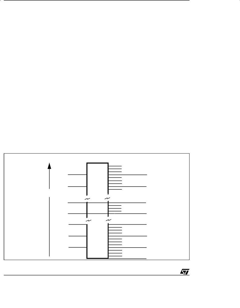
Figure 1. ST90158 Block Diagram
|
|
|
|
ADDRESS |
|
|
|
|
DATA |
|
|
|
|
Port0 |
|
EPROM/ |
|
|
|
|
ROM/OTP |
|
|
ADDRESS |
|
up to 64 Kbytes |
|
|
|
|
|
|
|
Port1 |
|
RAM |
|
|
|
|
up to 2 Kbytes |
|
|
|
|
|
|
|
Fully Prog. |
AS |
|
|
|
I/Os |
WAIT |
256 bytes |
BUS |
|
|
NMI |
|
|
||
R/W |
Register File |
MEMORY |
|
STIM |
DS |
8/16 bits |
|
||
|
|
|
||
|
|
|
|
|
|
CPU |
|
|
|
|
Interrupt |
|
|
|
INT0-7 |
Management |
|
|
|
|
|
|
SPI |
|
|
|
|
|
|
|
ST9+ CORE |
|
|
I2C/IM Bus |
OSCIN |
|
|
|
|
OSCOUT |
|
|
|
|
RESET |
RCCU |
|
|
|
INTCLK |
|
|
|
|
|
|
|
A/D |
|
CKAF |
|
|
BUS |
|
|
|
Converter |
||
WDIN |
|
|
||
|
|
|
||
WATCHDOG |
|
REGISTER |
with analog |
|
T0OUTB |
|
|
||
WDOUT |
|
|
watchdog |
|
HW0SW1 |
|
|
|
|
T0OUTA |
|
|
|
|
T0INA |
MFT0 |
|
|
SCI0 |
|
|
|
||
|
|
|
|
|
T0INB |
|
|
|
|
T1OUTA |
MFT1 |
|
|
|
T1OUTB |
|
|
|
|
T1INA |
|
|
|
|
T1INB |
|
|
|
SCI1 |
T3OUTA |
|
|
|
|
MFT3 |
|
|
|
|
T3OUTB |
|
|
|
|
|
|
|
|
|
T3INA |
|
|
|
|
T3INB |
|
|
|
|
All alternate functions (Italic characters) are mapped on Port2 through Port9
P0[7:0]
P1[7:0]
P0[7:0]
P1[7:0]
P2[6:0]
P4[7:0] P5[7:3], P5.1 P6[6:0] P7[7:0] P8[7:0]
P9[7:4], P9[2:0]
STOUT
SDI
SDO
SCK
EXTRG
AIN[7:0]
TX0CKIN
RX0CKIN
S0IN
DCD0
S0OUT
CLK0OUT
RTS0
TX1CKIN
RX1CKIN
S1IN
DCD1
S1OUT
CLK1OUT
RTS1
8/190

Figure 2. ST90135 Block Diagram
ROM up to 32 Kbytes
|
RAM |
|
|
up to 1 Kbyte |
|
AS |
|
|
WAIT |
256 bytes |
|
NMI |
||
R/W |
Register File |
|
DS |
8/16 bits |
|
|
||
|
CPU |
|
|
Interrupt |
|
INT0-7 |
Management |
|
|
||
|
ST9+ CORE |
|
OSCIN |
|
|
OSCOUT |
|
|
RESET |
RCCU |
|
INTCLK |
||
|
||
CKAF |
|
|
WDIN |
|
|
WDOUT |
WATCHDOG |
|
HW0SW1 |
|
|
T1OUTA |
|
|
T1OUTB |
MFT1 |
|
T1INA |
||
T1INB |
|
|
T3OUTA |
|
|
T3OUTB |
MFT3 |
|
T3INA |
||
|
||
T3INB |
|
ST90158 - GENERAL DESCRIPTION
|
ADDRESS |
|
|
|
DATA |
P0[7:0] |
|
|
Port0 |
|
|
|
ADDRESS |
P1[7:0] |
|
|
Port1 |
|
|
|
|
P0[7:0] |
|
|
|
P1[7:0] |
|
|
|
P2[6:0] |
|
|
|
P4[7:0] |
|
|
Fully Prog. |
P5[7:3], P5.1 |
|
|
I/Os |
P6[6:0] |
|
BUS |
|
P7[7:0] |
|
|
P8[7:0] |
||
MEMORY |
|
P9[7:4], P9[2:0] |
|
STIM |
STOUT |
||
|
|||
|
SPI |
SDI |
|
|
I2C/IM Bus |
SDO |
|
|
|
SCK |
|
BUS |
A/D |
EXTRG |
|
Converter |
|||
|
|||
|
AIN[7:0] |
||
REGISTER |
with analog |
||
|
|||
SCI0 |
|
||
|
watchdog |
|
|
|
|
TX0CKIN |
|
|
|
RX0CKIN |
|
|
|
S0IN |
|
|
|
DCD0 |
|
|
|
S0OUT |
|
|
|
CLK0OUT |
|
|
|
RTS0 |
All alternate functions (Italic characters) are mapped on Port2 through Port9
9/190

ST90158 - GENERAL DESCRIPTION
1.2 PIN DESCRIPTION
AS: Address Strobe (output, active low, 3-state). Address Strobe is pulsed low once at the beginning of each memory cycle. The rising edge of AS indicates that address, Read/Write (R/W), and Data Memory signals are valid for memory transfers. Under program control, AS can be placed in a high-impedance state along with Port 0, Port 1 and Data Strobe (DS).
DS: Data Strobe (output, active low, 3-state). Data Strobe provides the timing for data movement to or from Port 0 for each memory transfer. During a write cycle, data out is valid at the leading edge of DS. During a read cycle, Data In must be valid prior to the trailing edge of DS. When the ST90158 accesses on-chip memory, DS is held high during the whole memory cycle. It can be placed in a high impedance state along with Port 0, Port 1 and AS.
RESET: Reset (input, active low). The ST9+ is initialised by the Reset signal. With the deactivation of RESET, program execution begins from the memory location pointed to by the vector contained in memory locations 00h and 01h.
R/W: Read/Write (output, 3-state). Read/Write determines the direction of data transfer for external memory transactions. R/W is low when writing to external memory, and high for all other transactions. It can be placed in high impedance state along with Port 0, Port 1, AS and DS.
OSCIN, OSCOUT: Oscillator (input and output). These pins connect a parallel-resonant crystal (3
to 5 MHz), or an external source to the on-chip clock oscillator and buffer. OSCIN is the input of the oscillator inverter and internal clock generator; OSCOUT is the output of the oscillator inverter.
HW0_SW1: When connected to VDD through a 1K pull-up resistor, the software watchdog option is selected. When connected to VSS through a 1K pull-down resistor, the hardware watchdog option is selected.
VPP: Programming voltage for EPROM/OTP devices. Must be connected to VSS in user mode through a 10 Kohm resistor.
AVDD: Analog VDD of the Analog to Digital Converter.
AVSS: Analog VSS of the Analog to Digital Converter.
VDD: Main Power Supply Voltage (5V ± 10%).
VSS: Digital Circuit Ground.
P0[7:0], P1[7:0]: (Input/Output, TTL or CMOS compatible). 16 lines grouped into I/O ports providing the external memory interface for addressing 64Kbytes of external memory.
P0[7:0], P1[7:0], P2[6:0], P4[7:0], P5[7:3], P5.1, P6[6:0], P7[7:0], P8[7:0], P9[7:4], P9[2:0]: I/O Port Lines (Input/Output, TTL or CMOS compatible). I/O lines grouped into I/O ports of 8 bits, bit programmable under program control as general purpose I/O or as alternate functions.
10/190
ST90158 - GENERAL DESCRIPTION
PIN DESCRIPTION (Cont'd)
Figure 3. 80-Pin TQFP Pin-out
AD6/P0.6
VSS
AD7/P0.7
VDD
AS
DS
VPP*
P4.0
P4.1 INTCLK/P4.2 STOUT/P4.3 WDOUT/I NT0/P4.4 INT4/P4.5 T0OUTB/INT5 /P4.6 T0OUTA/P4.7 P2.0 P2.1 P2.2 P2.3 P2.4
P0.5/AD5 |
P0.4/AD4 |
P0.3/AD3 |
P0.2/AD2 |
P0.1/AD1 |
P0.0/AD0 |
P6.6 |
P6.5/RW |
P6.4 |
P6.3 |
P6.2 |
P6.1 |
P6.0 |
P1.7/A15 |
P1.6/A14 |
P1.5/A13 |
P1.4/A12 |
P1.3/A11 |
P1.2/A10 |
P1.1/A9 |
80 |
|
|
|
|
|
|
|
|
|
|
|
|
|
|
|
|
|
|
61 |
1 |
|
|
|
|
|
|
|
|
|
|
|
|
|
|
|
|
|
|
60 |
ST90158/ST90135
20 |
|
|
|
|
|
|
|
|
|
|
|
|
|
|
|
|
|
|
41 |
21 |
|
|
|
|
|
|
|
|
|
|
|
|
|
|
|
|
|
|
40 |
P2.5 |
P2.6 |
S1OUT/P9.0 |
T0OUTB/S1IN/P9.1 |
TX1CKIN/CLK1OUT/P9.2 |
S0OUT/RX1CKIN/P9.4 |
S0IN/P9.5 |
INT2/SCK/P9.6 |
INT6/SDO/P9.7 |
AIN0/RX0CKIN/WDIN/EXTRG/P7.0 |
AIN1/T0INB/SDI/P7.1 |
AIN2/CLK0OUT/TX0CKIN/P7.2 |
AIN3/T0INA/P7.3 |
AIN4/P7.4 |
AIN5/P7.5 |
AIN6/P7.6 |
AIN7/P7.7 |
DD |
SS |
NMI/T3OUTB/P8.7 |
AV |
AV |
P1.0/A8
RESET
OSCIN
VSS
OSCOUT
P5.1/SDI
HW0SW1
P5.3
P5.4/T1OUTA/DCD0
P5.5/T1OUT1/RTS0
P5.6/T3OUTA/DCD1 P5.7/T3OUTB/RTS1/CKAF
VDD
P8.0/T3INA
P8.1/T1INB
P8.2/INT1/T1OUTA
P8.3/INT3/T1OUTB P8.4/T1INA/WA IT/WDOUT P8.5/T3INB P8.6/INT7/T3OUTA
*EPROM or OTP devices only
11/190
ST90158 - GENERAL DESCRIPTION
PIN DESCRIPTION (Cont'd)
Figure 4. 80-Pin PQFP Pin-Out
AD4/P0.4
AD5/P0.5
AD6/P0.6
VSS
AD7/P0.7
VDD
AS
DS
VPP*
P4.0
P4.1
INTCLK/P4.2
STOUT/P4.3
INT0/WDOUT/P4.4
INT4/P4.5
INT5/T0OUTB/P4.6
T0OUTA/P4.7
P2.0
P2.1
P2.2
P2.3
P2.4
P2.5
P2.6
P0.3/AD3 |
P0.2/AD2 P0.1/AD1 P0.0/AD0 |
P6.6 P6.5/RW |
P6.4 P6.3 P6.2 |
P6.1 P6.0 |
P1.7/A15 P1.6/A14 P1.5/A13 |
80 |
|
|
|
|
|
1
ST90158/ST90135
24 |
|
|
|
|
|
|
|
|
|
|
|
|
|
S1OUT/P9.0 |
T0OUTB/S1IN/P9.1 |
TX1CKIN/CLK1OUT/P9.2 |
S0OUT/RX1CKIN/P9.4 |
S0IN/P9.5 |
INT2/SCK/P9.6 |
INT6/SDO/P9.7 |
AIN0/RX0CKIN/WDIN/EXTRG/P7.0 |
AIN1/T0INB/P7.1 |
AIN2/CLK0OUT/TX0CKIN/P7.2 |
AIN3/T0INA/P7.3 |
AIN4/P7.4 |
AIN5/P7.5 |
AIN6/P7.6 |
P1.4/A12 |
P1.3/A11 |
64P1.2/A10
P1.1/A9
P1.0/A8 RESET OSCIN
VSS
OSCOUT P5.1/SDI HW0SW1 P5.3
P5.4/T1OUTA/DCD0
P5.5/T1OUTB/RTS0
P5.6/T3OUTA/DCD1 P5.7/T3OUTB/RTS1/CK_AF
VDD
P8.0/T3INA
P8.1/T1INB
P8.2/T1OUTA/INT1
P8.3/T1OUTB/INT3 P8.4/T1INA/WAIT/WDOUT P8.5/T3INB P8.6/INT7/T3OUTA P8.7/NMI/T3OUTB
40 AVSS
AIN7/P7.7 |
DD |
AV |
*EPROM or OTP devices only
12/190
ST90158 - GENERAL DESCRIPTION
1.3 I/O PORT PINS
All the ports of the device can be programmed as Input/Output or in Input mode, compatible with TTL or CMOS levels (except where Schmitt Trigger is present). Each bit can be programmed individually (Refer to the I/O ports chapter).
TTL/CMOS Input
For all those port bits where no input schmitt trigger is implemented, it is always possible to program the input level as TTL or CMOS compatible by programming the relevant PxC2.n control bit.
Refer to the section titled ªInput/Output Bit Configurationº in the I/O Ports Chapter .
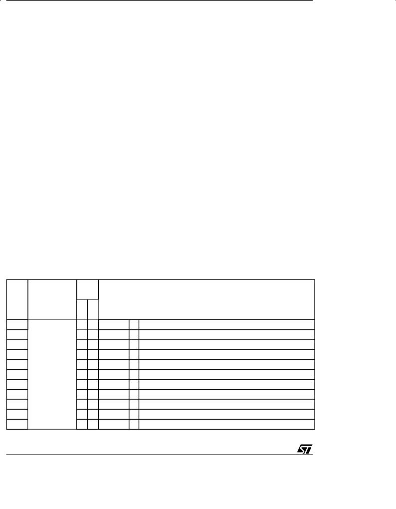
Table 1. I/O Port Characteristics
|
Input |
Output |
Port 0 |
TTL/CMOS |
Push-Pull/OD |
Port 1 |
TTL/CMOS |
Push-Pull/OD |
Port 2 |
TTL/CMOS |
Push-Pull/OD |
Port 4 |
Schmitt trigger |
Push-Pull/OD |
Port 5 |
Schmitt trigger |
Push-Pull/OD |
Port 6 |
TTL/CMOS |
Push-Pull/OD |
Port 7 |
Schmitt trigger |
Push-Pull/OD |
Port 8 |
Schmitt trigger |
Push-Pull/OD |
Port 9 |
Schmitt trigger |
Push-Pull/OD |
Legend: WPU = Weak Pull-Up, OD = Open Drain
Push-Pull/OD Output
The output buffer can be programmed as pushpull or open-drain: attention must be paid to the fact that the open-drain option corresponds only to a disabling of P-channel MOS transistor of the buffer itself: it is still present and physically connected to the pin. Consequently it is not possible to increase the output voltage on the pin over VDD+0.3 Volt, to avoid direct junction biasing.
Weak Pull-Up |
Reset State |
Yes |
Bidirectional WPU |
Yes |
Bidirectional WPU |
No |
Bidirectional |
Yes |
Bidirectional WPU |
Yes |
Bidirectional WPU |
No |
Bidirectional |
Yes |
Bidirectional WPU |
Yes |
Bidirectional WPU |
Yes |
Bidirectional WPU |
13/190
ST90158 - GENERAL DESCRIPTION
I/O PORT PINS (Cont'd)
How to Configure the I/O ports
To configure the I/O ports, use the information in Table 1, Table 2 and the Port Bit Configuration Table in the I/O ports Chapter (See page 92).
Input Note = the hardware characteristics fixed for each port line in Table 1.
±If Input note = TTL/CMOS, either TTL or CMOS input level can be selected by software.
±If Input note = Schmitt trigger, selecting CMOS or TTL input by software has no effect, the input will always be Schmitt Trigger.
Alternate Functions (AF) = More than one AF cannot be assigned to an I/O pin at the same time:
An alternate function can be selected as follows.
AF Inputs:
± AF is selected implicitly by enabling the corresponding peripheral. Exception to this are A/D inputs which must be explicitly selected as AF by software.
AF Outputs or Bidirectional Lines:
± In the case of Outputs or I/Os, AF is selected explicitly by software.
Example 1: SCI data input
AF: S0IN, Port: P9.5, Port Style: Input Schmitt
Trigger.
Write the port configuration bits:
P9C2.5=1
P9C1.5=0
P9C0.5=1
Enable the SCI peripheral by software as described in the SCI chapter.
Example 2: SCI data output
AF: S0OUT, Port: P9.4 Output push-pull (configured by software).
Write the port configuration bits:
P9C2.4=0
P9C1.4=1
P9C0.4=1
Example 3: ADC data input
AF: AIN0, Port : P7.0, Input Note: does not apply to ADC
Write the port configuration bits:
P7C2.0=1
P7C1.0=1
P7C0.0=1
Example 4: External Memory I/O
AF: AD0, Port : P0.0
Write the port configuration bits:
P0C2.0=0
P0C1.0=1
P0C0.0=1
Table 2. I/O Port Description and Alternate Functions
Port General
Name Purpose I/O
P0.0
P0.1
P0.2
P0.3
P0.4
All ports useable
for general purP0.5 pose I/O (input,
P0.6
output or bidirectional)
P0.7
P1.0
P1.1
P1.2
Pin
No.
TQFP |
PQFP |
|
|
Alternate Functions |
|
|
|
||
75 |
77 |
AD0 |
I/O |
Address/Data bit 0 mux |
76 |
78 |
AD1 |
I/O |
Address/Data bit 1 mux |
77 |
79 |
AD2 |
I/O |
Address/Data bit 2 mux |
78 |
80 |
AD3 |
I/O |
Address/Data bit 3 mux |
79 |
1 |
AD4 |
I/O |
Address/Data bit 4 mux |
80 |
2 |
AD5 |
I/O |
Address/Data bit 5 mux |
1 |
3 |
AD6 |
I/O |
Address/Data bit 6 mux |
3 |
5 |
AD7 |
I/O |
Address/Data bit 7 mux |
60 |
62 |
A8 |
I/O |
Address bit 8 |
61 |
63 |
A9 |
I/O |
Address bit 9 |
62 |
64 |
A10 |
I/O |
Address bit 10 |
14/190
ST90158 - GENERAL DESCRIPTION
Port |
General |
Name |
Purpose I/O |
Pin
No.
Alternate Functions
TQFP |
PQFP |
P1.3 |
|
P1.4 |
|
P1.5 |
|
P1.6 |
|
P1.7 |
|
P2.0 |
|
P2.1 |
|
P2.2 |
|
P2.3 |
|
P2.4 |
|
P2.5 |
|
P2.6 |
|
P4.0 |
|
P4.1 |
|
P4.2 |
|
P4.3 |
All ports useable |
|
for general pur- |
P4.4 |
pose I/O (input, |
|
output or bidirec- |
P4.5 |
tional) |
P4.6 |
|
P4.7
P5.1
P5.3
P5.4
P5.5
P5.6
P5.7
P6.0
63 |
65 |
A11 |
I/O |
Address bit 11 |
|
64 |
66 |
A12 |
I/O |
Address bit 12 |
|
65 |
67 |
A13 |
I/O |
Address bit 13 |
|
66 |
68 |
A14 |
I/O |
Address bit 14 |
|
67 |
69 |
A15 |
I/O |
Address bit 15 |
|
16 |
18 |
|
I/O |
|
|
17 |
19 |
|
I/O |
|
|
18 |
20 |
|
I/O |
|
|
19 |
21 |
|
I/O |
|
|
20 |
22 |
|
I/O |
|
|
21 |
23 |
|
I/O |
|
|
22 |
24 |
|
I/O |
|
|
8 |
10 |
|
I/O |
|
|
9 |
11 |
|
I/O |
|
|
10 |
12 |
INTCLK |
O |
Internal main Clock |
|
11 |
13 |
STOUT |
O |
Standard Timer Output |
|
12 |
14 |
INT0 |
I |
External Interrupt 0 |
|
WDOUT |
O |
Watchdog Timer output |
|||
|
|
||||
13 |
15 |
INT4 |
I |
External interrupt 4 |
|
14 |
16 |
INT5 |
I |
External Interrupt 5 |
|
T0OUTB |
O |
MF Timer 0 Output B 1) |
|||
|
|
||||
15 |
17 |
T0OUTA |
O |
MF Timer 0 Output A 1) |
|
55 |
57 |
SDI |
I |
SPI Serial Data In |
|
53 |
55 |
|
I/O |
|
|
52 |
54 |
T1OUTA |
O |
MF Timer 1 output A |
|
DCD0 |
I |
SCI0 Data Carrier Detect |
|||
|
|
||||
51 |
53 |
RTS0 |
O |
SCI0 Request to Send |
|
T1OUTB |
O |
MF Timer 1 output B |
|||
|
|
||||
50 |
52 |
T3OUTA |
O |
MF Timer 3 output A |
|
DCD1 |
I |
SCI1 Data Carrier Detect 1) |
|||
|
|
||||
|
|
RTS1 |
O |
SCI1 Request to Send 1) |
|
49 |
51 |
T3OUTB |
O |
MF Timer 3 output B |
|
|
|
CK_AF |
I |
External Clock Input |
|
68 |
70 |
|
I/O |
|
15/190

ST90158 - GENERAL DESCRIPTION
Port |
General |
Name |
Purpose I/O |
Pin
No.
Alternate Functions
TQFP |
PQFP |
P6.1
P6.2
P6.3
P6.4
P6.5
P6.6
P7.0
P7.1
P7.2
P7.3
P7.4
P7.5
P7.6
P7.7
P8.0
P8.1
P8.2
P8.3
P8.4
P8.5
P8.6
P8.7
All ports useable for general purpose I/O (input, output or bidirectional)
69 |
71 |
|
I/O |
|
|
70 |
72 |
|
I/O |
|
|
71 |
73 |
|
I/O |
|
|
72 |
74 |
|
I/O |
|
|
73 |
75 |
R/W |
O |
Read/Write |
|
74 |
76 |
|
I/O |
|
|
|
|
AIN0 |
I |
A/D Analog input 0 |
|
30 |
32 |
RX0CKIN |
I |
SCI0 Receive Clock input |
|
WDIN |
I |
T/WD input |
|||
|
|
||||
|
|
EXTRG |
I |
A/D External Trigger |
|
|
|
AIN1 |
I |
A/D Analog input 1 |
|
31 |
33 |
T0INB |
I |
MF Timer 0 input B 1) |
|
|
|
SDI |
I |
SPI Serial Data In |
|
|
|
AIN2 |
I |
A/D Analog input 2 |
|
32 |
34 |
CLK0OUT |
O |
SCI0 Byte Sync Clock output |
|
|
|
TX0CKIN |
I |
SCI0 Transmit Clock input |
|
33 |
35 |
AIN3 |
I |
A/D Analog input 3 |
|
T0INA |
I |
MF Timer 0 input A 1) |
|||
|
|
||||
34 |
36 |
AIN4 |
I |
A/D Analog input 4 |
|
35 |
37 |
AIN5 |
I |
A/D Analog input 5 |
|
36 |
38 |
AIN6 |
I |
A/D Analog input 6 |
|
37 |
39 |
AIN7 |
I |
A/D Analog input 7 |
|
47 |
49 |
T3INA |
I |
MF Timer 3 input A |
|
46 |
48 |
T1INB |
I |
MF Timer 1 input B |
|
45 |
47 |
INT1 |
I |
External interrupt 1 |
|
T1OUTA |
O |
MF Timer 1 output A |
|||
|
|
||||
44 |
46 |
INT3 |
I |
External interrupt 3 |
|
T1OUTB |
O |
MF Timer 1 output B |
|||
|
|
||||
|
|
T1INA |
I |
MF Timer 1 input A |
|
43 |
45 |
WAIT |
I |
External Wait input |
|
|
|
WDOUT |
O |
Watchdog Timer output |
|
42 |
44 |
T3INB |
I |
MF Timer 3 input B |
|
41 |
43 |
INT7 |
I |
External interrupt 7 |
|
T3OUTA |
O |
MF Timer 3 output A |
|||
|
|
||||
40 |
42 |
NMI |
I |
Non-Maskable Interrupt |
|
T3OUTB |
O |
MF Timer 3 output B |
|||
|
|
16/190
ST90158 - GENERAL DESCRIPTION
Port |
General |
Name |
Purpose I/O |
P9.0 |
|
P9.1 |
|
P9.2 |
All ports useable |
|
|
|
for general pur- |
P9.4 |
pose I/O (input, |
|
output or bidirec- |
P9.5 |
tional) |
P9.6 |
|
P9.7 |
|
Pin |
|
|
|
||
No. |
|
|
|
||
TQFP |
PQFP |
|
|
Alternate Functions |
|
|
|
|
|||
23 |
25 |
S1OUT |
O |
SCI1 Serial Output 1) |
|
24 |
26 |
T0OUTB |
O |
MF Timer 0 output B 1) |
|
S1IN |
I |
SCI1 Serial Input 1) |
|||
|
|
||||
25 |
27 |
CLK1OUT |
O |
SCI1 Byte Sync Clock output 1) |
|
TX1CKIN |
I |
SCI1 Transmit Clock input 1) |
|||
|
|
||||
26 |
28 |
S0OUT |
O |
SCI0 Serial Output |
|
RX1CKIN |
O |
SCI1 Receive Clock input 1) |
|||
|
|
||||
27 |
29 |
S0IN |
I |
SCI0 Serial Input |
|
28 |
30 |
INT2 |
I |
External interrupt 2 |
|
SCK |
O |
SPI Serial Clock |
|||
|
|
||||
29 |
31 |
INT6 |
I |
External interrupt 6 |
|
SDO |
O |
SPI Serial Data Out |
|||
|
|
||||
Note 1) Not present on ST90135
17/190
ST90158 - DEVICE ARCHITECTURE
2 DEVICE ARCHITECTURE
2.1 CORE ARCHITECTURE
The ST9+ Core or Central Processing Unit (CPU) features a highly optimised instruction set, capable of handling bit, byte (8-bit) and word (16-bit) data, as well as BCD and Boolean formats; 14 addressing modes are available.
Four independent buses are controlled by the Core: a 16-bit Memory bus, an 8-bit Register data bus, an 8-bit Register address bus and a 6-bit Interrupt/DMA bus which connects the interrupt and DMA controllers in the on-chip peripherals with the Core.
This multiple bus architecture affords a high degree of pipelining and parallel operation, thus making the ST9+ family devices highly efficient, both for numerical calculation, data handling and with regard to communication with on-chip peripheral resources.
2.2 MEMORY SPACES
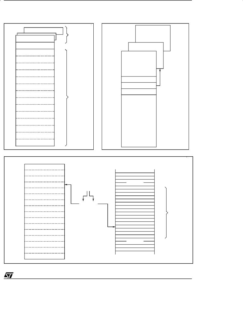
There are two separate memory spaces:
± The Register File, which comprises 240 8-bit registers, arranged as 15 groups (Group 0 to E), each containing sixteen 8-bit registers plus up to 64 pages of 16 registers mapped in Group F,
which hold data and control bits for the on-chip peripherals and I/Os.
± A single linear memory space accommodating both program and data. All of the physically separate memory areas, including the internal ROM, internal RAM and external memory are mapped in this common address space. The total addressable memory space of 4 Mbytes (limited by the size of on-chip memory and the number of external address pins) is arranged as 64 segments of 64 Kbytes. Each segment is further subdivided into four pages of 16 Kbytes, as illustrated in Figure 5. A Memory Management Unit uses a set of pointer registers to address a 22-bit memory field using 16-bit address-based instructions.
2.2.1 Register File
The Register File consists of (see Figure 6):
±224 general purpose registers (Group 0 to D, registers R0 to R223)
±6 system registers in the System Group (Group E, registers R224 to R239)
±Up to 64 pages, depending on device configuration, each containing up to 16 registers, mapped to Group F (R240 to R255), see Figure 7.
|
|
Data |
Code |
Address |
|
16K Pages |
64K Segments |
3FFFFFh |
|
255 |
|
|
|
254 |
63 |
|
|
253 |
|
3F0000h |
|
|
|
|
252 |
|
|
3EFFFFh |
|
251 |
|
|
|
250 |
62 |
3E0000h |
|
249 |
|
|
248 |
|
|
|
|
247 |
|
up to 4 Mbytes |
|
|
|
21FFFFh |
|
135 |
|
Reserved |
134 |
|
|
|
33 |
||
|
133 |
||
210000h |
|
||
|
132 |
|
|
20FFFFh |
|
|
|
02FFFFh |
|
11 |
|
|
10 |
|
|
|
|
2 |
|
020000h |
|
9 |
|
|
|
||
|
8 |
|
|
01FFFFh |
|
7 |
|
|
6 |
1 |
|
|
|
||
010000h |
|
5 |
|
|
|
||
|
4 |
|
|
00FFFFh |
|
3 |
|
Figure 5. Single Program and Data Memory Address Space |
2 |
|
|
|
|
000000h |
1 |
0 |
|
||
0 |
|
|
|
|
18/190
|
|
|
|
ST90158 - DEVICE ARCHITECTURE |
|
MEMORY SPACES (Cont'd) |
|
|
|
||
Figure 6. Register Groups |
|
Figure 7. Page Pointer for Group F mapping |
|||
|
|
|
UP TO |
|
PAGE 63 |
255 |
|
|
|
|
|
|
|
64 PAGES |
|
|
|
240 F PAGED REGISTERS |
|
|
|||
|
|
|
|||
239 |
E SYSTEM REGISTERS |
|
|
PAGE 5 |
|
224 |
|
|
|||
223 |
D |
|
|
R255 |
|
|
C |
|
|
|
PAGE 0 |
|
|
|
|
|
|
|
B |
|
|
|
|
|
A |
|
|
R240 |
|
|
|
|
|
|
|
|
9 |
|
|
|
|
|
8 |
|
|
R234 |
PAGE POINTER |
|
|
224 |
|
|
|
|
7 |
|
R224 |
|
|
|
|
GENERAL |
|
||
|
|
|
|
|
|
|
6 |
|
PURPOSE |
|
|
|
|
REGISTERS |
|
|
|
|
|
|
|
|
|
|
5 |
|
|
|
|
|
4 |
|
|
|
|
|
3 |
|
|
|
|
|
2 |
|
|
|
|
|
1 |
|
|
|
|
|
0 |
15 |
|
|
|
0 |
0 |
VA00432 |
R0 |
|
|
|
VA00433 |
||||
Figure 8. Addressing the Register File |
|
|
|||
|
|
REGISTER FILE |
|
|
|
|
255 |
F PAGED REGISTERS |
|
|
|
|
240 |
|
|
|
|
|
|
|
|
|
|
|
239 |
E SYSTEM REGISTERS |
|
|
|
|
224 |
|
|
|
|
|
|
|
|
|
|
|
223 |
D |
|
|
|
|
|
|
|
GROUP D |
|
|
|
C |
R195 |
|
|
|
|
|
R207 |
||
|
|
|
|
||
|
|
|
(R0C3h) |
|
|
|
|
B |
|
|
|
|
|
|
|
|
|
|
|
A |
|
|
|
|
|
9 |
(1100) (0011) |
|
|
|
|
|
|
|
|
|
|
8 |
|
|
|
|
|
7 |
|
|
GROUP C |
|
|
|
|
|
|
|
|
6 |
|
|
|
|
|
5 |
|
|
R195 |
|
|
4 |
|
|
|
|
|
3 |
|
|
R192 |
|
|
|
|
GROUP B |
|
|
|
2 |
|
|
|
|
|
|
|
|
|
|
|
1 |
|
|
|
|
|
0 |
15 |
|
|
|
0 |
0 |
|
|
|
|
|
|
VR000118 |
||
|
|
|
|
|
|
19/190
ST90158 - DEVICE ARCHITECTURE
MEMORY SPACES (Cont'd)
2.2.2 Register Addressing
Register File registers, including Group F paged registers (but excluding Group D), may be addressed explicitly by means of a decimal, hexadecimal or binary address; thus R231, RE7h and R11100111b represent the same register (see Figure 8). Group D registers can only be addressed in Working Register mode.
Note that an upper case ªRº is used to denote this direct addressing mode.
Working Registers
Certain types of instruction require that registers be specified in the form ªrxº, where x is in the range 0 to 15: these are known as Working Registers.
Note that a lower case ªrº is used to denote this indirect addressing mode.
Two addressing schemes are available: a single group of 16 working registers, or two separately mapped groups, each consisting of 8 working registers. These groups may be mapped starting at any 8 or 16 byte boundary in the register file by means of dedicated pointer registers. This technique is described in more detail in Section 2.3.3 Register Pointing Techniques, and illustrated in Figure 9 and in Figure 10.
System Registers
The 16 registers in Group E (R224 to R239) are System registers and may be addressed using any of the register addressing modes. These registers are described in greater detail in Section 2.3 SYSTEM REGISTERS.
Paged Registers
Up to 64 pages, each containing 16 registers, may be mapped to Group F. These are addressed using any register addressing mode, in conjunction with the Page Pointer register, R234, which is one of the System registers. This register selects the page to be mapped to Group F and, once set, does not need to be changed if two or more registers on the same page are to be addressed in succession.
Therefore if the Page Pointer, R234, is set to 5, the instructions:
spp #5
ld R242, r4
will load the contents of working register r4 into the third register of page 5 (R242).
These paged registers hold data and control information relating to the on-chip peripherals, each peripheral always being associated with the same pages and registers to ensure code compatibility between ST9+ devices. The number of these registers therefore depends on the peripherals which are present in the specific ST9+ family device. In other words, pages only exist if the relevant peripheral is present.
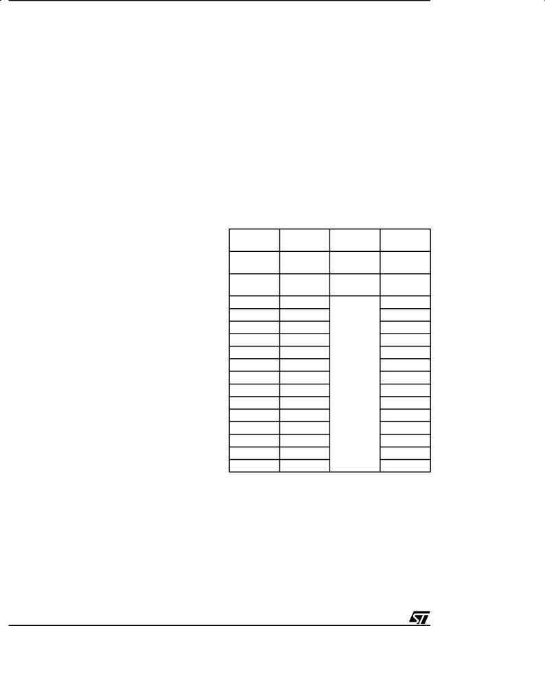
Table 3. Register File Organization
Hex. |
Decimal |
Function |
Register |
|
Address |
Address |
File Group |
||
|
||||
F0-FF |
240-255 |
Paged |
Group F |
|
Registers |
||||
|
|
|
||
E0-EF |
224-239 |
System |
Group E |
|
Registers |
||||
|
|
|
||
D0-DF |
208-223 |
|
Group D |
|
C0-CF |
192-207 |
|
Group C |
|
B0-BF |
176-191 |
|
Group B |
|
A0-AF |
160-175 |
|
Group A |
|
90-9F |
144-159 |
|
Group 9 |
|
80-8F |
128-143 |
|
Group 8 |
|
70-7F |
112-127 |
General |
Group 7 |
|
Purpose |
||||
60-6F |
96-111 |
Group 6 |
||
Registers |
||||
|
|
|
||
50-5F |
80-95 |
|
Group 5 |
|
40-4F |
64-79 |
|
Group 4 |
|
30-3F |
48-63 |
|
Group 3 |
|
20-2F |
32-47 |
|
Group 2 |
|
10-1F |
16-31 |
|
Group 1 |
|
00-0F |
00-15 |
|
Group 0 |
20/190
2.3 SYSTEM REGISTERS
The System registers are listed in Table 4. They are used to perform all the important system settings. Their purpose is described in the following pages. Refer to the chapter dealing with I/O for a description of the PORT[5:0] Data registers.
Table 4. System Registers (Group E)
R239 |
(EFh) |
SSPLR |
R238 |
(EEh) |
SSPHR |
R237 |
(EDh) |
USPLR |
R236 |
(ECh) |
USPHR |
R235 |
(EBh) |
MODE REGISTER |
R234 |
(EAh) |
PAGE POINTER REGISTER |
R233 |
(E9h) |
REGISTER POINTER 1 |
R232 |
(E8h) |
REGISTER POINTER 0 |
R231 |
(E7h) |
FLAG REGISTER |
R230 |
(E6h) |
CENTRAL INT. CNTL REG |
R229 |
(E5h) |
PORT5 DATA REG. |
R228 |
(E4h) |
PORT4 DATA REG. |
R227 |
(E3h) |
PORT3 DATA REG. |
R226 |
(E2h) |
PORT2 DATA REG. |
R225 |
(E1h) |
PORT1 DATA REG. |
R224 |
(E0h) |
PORT0 DATA REG. |
2.3.1 Central Interrupt Control Register
Please refer to the ºINTERRUPTº chapter for a detailed description of the ST9 interrupt philosophy.
CENTRAL INTERRUPT CONTROL REGISTER (CICR)
R230 - Read/Write Register Group: E (System)
Reset Value: 1000 0111 (87h)
7 |
0 |
GCE TLIP TLI IEN IAM CPL2 CPL1 CPL0 N
Bit 7 = GCEN: Global Counter Enable.
This bit is the Global Counter Enable of the Multifunction Timers. The GCEN bit is ANDed with the CE bit in the TCR Register (only in devices featuring the MFT Multifunction Timer) in order to enable the Timers when both bits are set. This bit is set after the Reset cycle.
ST90158 - DEVICE ARCHITECTURE
Note: If an MFT is not included in the ST9 device, then this bit has no effect.
Bit 6 = TLIP: Top Level Interrupt Pending.
This bit is set by hardware when a Top Level Interrupt Request is recognized. This bit can also be set by software to simulate a Top Level Interrupt Request.
0:No Top Level Interrupt pending
1:Top Level Interrupt pending
Bit 5 = TLI: Top Level Interrupt bit.
0:Top Level Interrupt is acknowledged depending on the TLNM bit in the NICR Register.
1:Top Level Interrupt is acknowledged depending on the IEN and TLNM bits in the NICR Register (described in the Interrupt chapter).
Bit 4 = IEN: Interrupt Enable .
This bit is cleared by interrupt acknowledgement, and set by interrupt return (iret). IEN is modified implicitly by iret, ei and di instructions or by an interrupt acknowledge cycle. It can also be explicitly written by the user, but only when no interrupt is pending. Therefore, the user should execute a di instruction (or guarantee by other means that no interrupt request can arrive) before any write operation to the CICR register.
0:Disable all interrupts except Top Level Interrupt.
1:Enable Interrupts
Bit 3 = IAM: Interrupt Arbitration Mode.
This bit is set and cleared by software to select the arbitration mode.
0:Concurrent Mode
1:Nested Mode.
Bit 2:0 = CPL[2:0]: Current Priority Level.
These three bits record the priority level of the routine currently running (i.e. the Current Priority Level, CPL). The highest priority level is represented by 000, and the lowest by 111. The CPL bits can be set by hardware or software and provide the reference according to which subsequent interrupts are either left pending or are allowed to interrupt the current interrupt service routine. When the current interrupt is replaced by one of a higher priority, the current priority value is automatically stored until required in the NICR register.
21/190
ST90158 - DEVICE ARCHITECTURE
SYSTEM REGISTERS (Cont'd)
2.3.2 Flag Register
The Flag Register contains 8 flags which indicate the CPU status. During an interrupt, the flag register is automatically stored in the system stack area and recalled at the end of the interrupt service routine, thus returning the CPU to its original status.
This occurs for all interrupts and, when operating in nested mode, up to seven versions of the flag register may be stored.
FLAG REGISTER (FLAGR)
R231Read/Write
Register Group: E (System)
Reset value: 0000 0000 (00h)
7 |
|
|
|
|
|
0 |
C |
Z |
S |
V |
DA H |
- |
DP |
Bit 7 = C: Carry Flag.
The carry flag is affected by:
Addition (add, addw, adc, adcw), Subtraction (sub, subw, sbc, sbcw), Compare (cp, cpw),
Shift Right Arithmetic (sra, sraw), Shift Left Arithmetic (sla, slaw), Swap Nibbles (swap),
Rotate (rrc, rrcw, rlc, rlcw, ror, rol),
Decimal Adjust (da),
Multiply and Divide (mul, div, divws).
When set, it generally indicates a carry out of the most significant bit position of the register being used as an accumulator (bit 7 for byte operations and bit 15 for word operations).
The carry flag can be set by the Set Carry Flag (scf) instruction, cleared by the Reset Carry Flag (rcf) instruction, and complemented by the Complement Carry Flag (ccf) instruction.
Bit 6 = Z: Zero Flag. The Zero flag is affected by: Addition (add, addw, adc, adcw), Subtraction (sub, subw, sbc, sbcw), Compare (cp, cpw),
Shift Right Arithmetic (sra, sraw), Shift Left Arithmetic (sla, slaw), Swap Nibbles (swap),
Rotate (rrc, rrcw, rlc, rlcw, ror, rol),
Decimal Adjust (da),
Multiply and Divide (mul, div, divws), Logical (and, andw, or, orw, xor, xorw, cpl),
Increment and Decrement (inc, incw, dec,
decw),
Test (tm, tmw, tcm, tcmw, btset).
In most cases, the Zero flag is setwhen the contents of the register being used as an accumulator become zero, following one of the above operations.
Bit 5 = S: Sign Flag.
The Sign flag is affected by the same instructions as the Zero flag.
The Sign flag is set when bit 7 (for a byte operation) or bit 15 (for a word operation) of the register used as an accumulator is one.
Bit 4 = V: Overflow Flag.
The Overflow flag is affected by the same instructions as the Zero and Sign flags.
When set, the Overflow flag indicates that a two's- complement number, in a result register, is in error, since it has exceeded the largest (or is less than the smallest), number that can be represented in two's-complement notation.
Bit 3 = DA: Decimal Adjust Flag.
The DA flag is used for BCD arithmetic. Since the algorithm for correcting BCD operations is different for addition and subtraction, this flag is used to specify which type of instruction was executed last, so that the subsequent Decimal Adjust (da) operation can perform its function correctly. The DA flag cannot normally be used as a test condition by the programmer.
Bit 2 = H: Half Carry Flag.
The H flag indicates a carry out of (or a borrow into) bit 3, as the result of adding or subtracting two 8-bit bytes, each representing two BCD digits. The H flag is used by the Decimal Adjust (da) instruction to convert the binary result of a previous addition or subtraction into the correct BCD result. Like the DA flag, this flag is not normally accessed by the user.
Bit 1 = Reserved bit (must be 0).
Bit 0 = DP: Data/Program Memory Flag.
This bit indicates the memory area addressed. Its value is affected by the Set Data Memory (sdm) and Set Program Memory (spm) instructions. Refer to the Memory Management Unit for further details.
22/190

SYSTEM REGISTERS (Cont'd)
If the bit is set, data is accessed using the Data Pointers (DPRs registers), otherwise it is pointed to by the Code Pointer (CSR register); therefore, the user initialization routine must include a Sdm instruction. Note that code is always pointed to by the Code Pointer (CSR).
Note: In the ST9+, the DP flag is only for compatibility with software developed for the first generation of ST9 devices. With the single memory addressing space, its use is now redundant. It must be kept to 1 with a Sdm instruction at the beginning of the program to ensure a normal use of the different memory pointers.
2.3.3 Register Pointing Techniques
Two registers within the System register group, are used as pointers to the working registers. Register Pointer 0 (R232) may be used on its own as a single pointer to a 16-register working space, or in conjunction with Register Pointer 1 (R233), to point to two separate 8-register spaces.
For the purpose of register pointing, the 16 register groups of the register file are subdivided into 32 8- register blocks. The values specified with the Set Register Pointer instructions refer to the blocks to be pointed to in twin 8-register mode, or to the lower 8-register block location in single 16-register mode.
The Set Register Pointer instructions srp, srp0 and srp1 automatically inform the CPU whether the Register File is to operate in single 16-register mode or in twin 8-register mode. The srp instruction selects the single 16-register group mode and
ST90158 - DEVICE ARCHITECTURE
specifies the location of the lower 8-register block, while the srp0 and srp1 instructions automatically select the twin 8-register group mode and specify the locations of each 8-register block.
There is no limitation on the order or position of these register groups, other than that they must start on an 8-register boundary in twin 8-register mode, or on a 16-register boundary in single 16register mode.
The block number should always be an even number in single 16-register mode. The 16-regis- ter group will always start at the block whose number is the nearest even number equal to or lower than the block number specified in the srp instruction. Avoid using odd block numbers, since this can be confusing if twin mode is subsequently selected.
Thus:
srp #3 will be interpreted as srp #2 and will allow using R16 ..R31 as r0 .. r15.
In single 16-register mode, the working registers are referred to as r0 to r15. In twin 8-register mode, registers r0 to r7 are in the block pointed to by RP0 (by means of the srp0 instruction), while registers r8 to r15 are in the block pointed to by RP1 (by means of the srp1 instruction).
Caution: Group D registers can only be accessed as working registers using the Register Pointers, or by means of the Stack Pointers. They cannot be addressed explicitly in the form ªRxxxº.
23/190

ST90158 - DEVICE ARCHITECTURE
SYSTEM REGISTERS (Cont'd)
POINTER 0 REGISTER (RP0)
R232 - Read/Write
Register Group: E (System)
Reset Value: xxxx xx00 (xxh)
7 |
0 |
RG4 RG3 RG2 RG1 RG0 RPS 0 |
0 |
POINTER 1 REGISTER (RP1)
R233 - Read/Write
Register Group: E (System)
Reset Value: xxxx xx00 (xxh)
7 |
0 |
RG4 RG3 RG2 RG1 RG0 RPS 0 |
0 |
Bit 7:3 = RG[4:0]: Register Group number.
These bits contain the number (in the range 0 to 31) of the register block specified in the srp0 or srp instructions. In single 16-register mode the number indicates the lower of the two 8-register blocks to which the 16 working registers are to be mapped, while in twin 8-register mode it indicates the 8-register block to which r0 to r7 are to be mapped.
Bit 2 = RPS: Register Pointer Selector.
This bit is set by the instructions srp0 and srp1 to indicate that the twin register pointing mode is selected. The bit is reset by the srp instruction to indicate that the single register pointing mode is selected.
0:Single register pointing mode
1:Twin register pointing mode
Bit 1:0: Reserved. Forced by hardware to zero.
This register is only used in the twin register pointing mode. When using the single register pointing mode, or when using only one of the twin register groups, the RP1 register must be considered as RESERVED and may NOT be used as a general purpose register.
Bit 7:3 = RG[4:0]: Register Group number. These bits contain the number (in the range 0 to 31) of the 8-register block specified in the srp1 instruction, to which r8 to r15 are to be mapped.
Bit 2 = RPS: Register Pointer Selector.
This bit is set by the srp0 and srp1 instructions to indicate that the twin register pointing mode is selected. The bit is reset by the srp instruction to indicate that the single register pointing mode is selected.
0:Single register pointing mode
1:Twin register pointing mode
Bit 1:0: Reserved. Forced by hardware to zero.
24/190
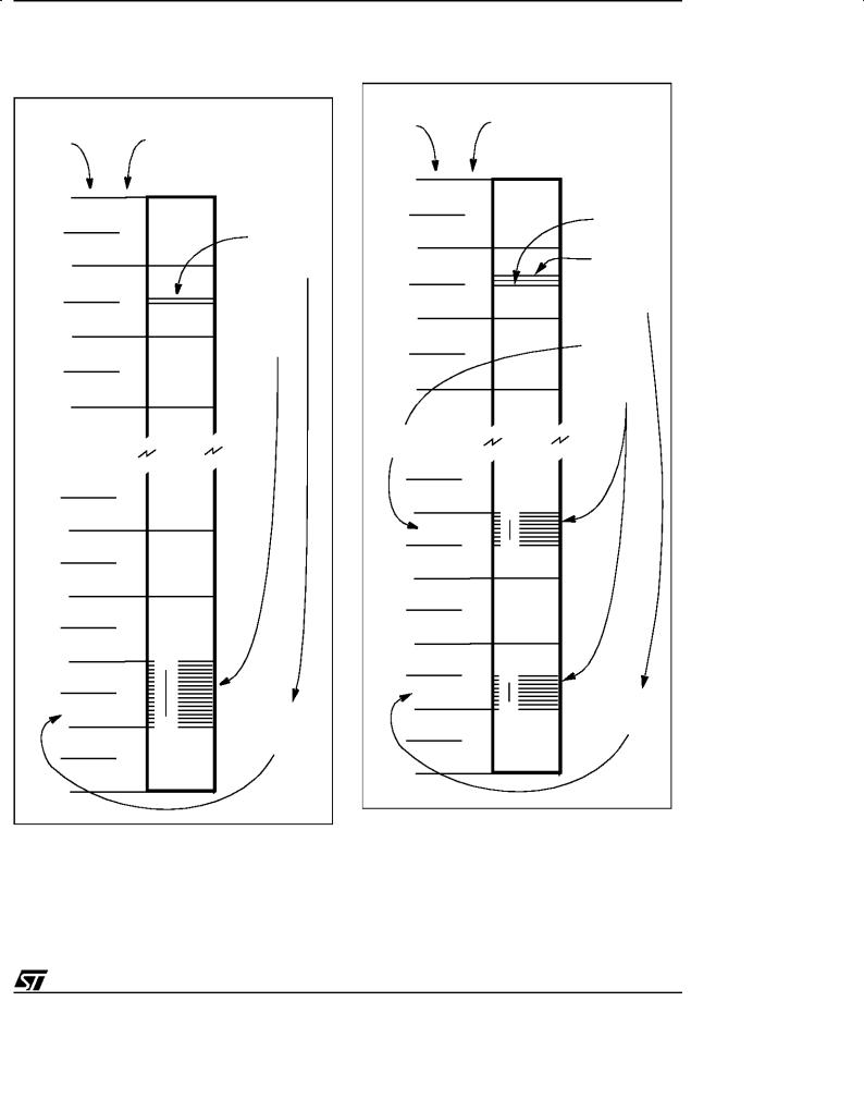
SYSTEM REGISTERS (Cont'd)
Figure 9. Pointing to a single group of 16 registers
REGISTER BLOCK GROUP NUMBER
REGIST ER
FILE
31
F
30
29
E
28
27
D
26
25
9
4
8
7
3
6
5
2
4
r15
3
1
2
r0
1
0
0
REGISTER POINTER 0 set by:
srp #2
instruction
points to:
GROUP 1
addressed by BLOCK 2
ST90158 - DEVICE ARCHITECTURE
Figure 10. Pointing to two groups of 8 registers
BLOCK
NUMBER
31
30
29
28
27
26
25
addressed by BLOCK 7
9
8
7
6
5
4
3
2
1
0
|
REGIST ER |
|
|
GROUP |
|
|
REGISTER |
|
|
FILE |
|
F |
|
REGISTER |
|
|
POINTE R 0 |
|
|
& |
|
|
REGIST ER |
|
|
POINTE R 1 |
E |
|
set by: |
|
|
|
|
|
srp0 #2 |
|
|
& |
D |
|
srp1 #7 |
|
|
|
|
|
instructions |
|
|
point to: |
4 |
|
|
|
r15 |
|
|
|
GROUP 3 |
3 |
r8 |
|
|
|
|
2 |
|
|
1 |
r7 |
|
|
|
GROUP 1 |
|
r0 |
addressed by |
|
|
BLOCK 2 |
0 |
|
|
25/190
ST90158 - DEVICE ARCHITECTURE
SYSTEM REGISTERS (Cont'd)
2.3.4 Paged Registers
Up to 64 pages, each containing 16 registers, may be mapped to Group F. These paged registers hold data and control information relating to the on-chip peripherals, each peripheral always being associated with the same pages and registers to ensure code compatibility between ST9+ devices. The number of these registers depends on the peripherals present in the specific ST9 device. In other words, pages only exist if the relevant peripheral is present.
The paged registers are addressed using the normal register addressing modes, in conjunction with the Page Pointer register, R234, which is one of the System registers. This register selects the page to be mapped to Group F and, once set, does not need to be changed if two or more registers on the same page are to be addressed in succession.
Thus the instructions:
spp #5
ld R242, r4
will load the contents of working register r4 into the third register of page 5 (R242).
Warning: During an interrupt, the PPR register is not saved automatically in the stack. If needed, it should be saved/restored by the user within the interrupt routine.
PAGE POINTER REGISTER (PPR)
R234 - Read/Write
Register Group: E (System)
Reset value: xxxx xx00 (xxh)
7 |
|
0 |
PP5 PP4 PP3 PP2 PP1 PP0 |
0 |
0 |
Bit 7:2 = PP[5:0]: Page Pointer.
These bits contain the number (in the range 0 to 63) of the page specified in the spp instruction. Once the page pointer has been set, there is no need to refresh it unless a different page is required.
Bit 1:0: Reserved. Forced by hardware to 0.
2.3.5 Mode Register
The Mode Register allows control of the following operating parameters:
±Selection of internal or external System and User Stack areas,
±Management of the clock frequency,
±Enabling of Bus request and Wait signals when interfacing to external memory.
MODE REGISTER (MODER)
R235 - Read/Write
Register Group: E (System)
Reset value: 1110 0000 (E0h)
7 |
0 |
SSP USP |
DIV2 PRS2 PRS1 PRS0 BRQEN HIMP |
Bit 7 = SSP: System Stack Pointer.
This bit selects an internal or external System Stack area.
0:External system stack area, in memory space.
1:Internal system stack area, in the Register File
(reset state).
Bit 6 = USP: User Stack Pointer.
This bit selects an internal or external User Stack area.
0:External user stack area, in memory space.
1:Internal user stack area, in the Register File (reset state).
Bit 5 = DIV2: OSCIN Clock Divided by 2.
This bit controls the divide-by-2 circuit operating on OSCIN.
0:Clock divided by 1
1:Clock divided by 2
Bit 4:2 = PRS[2:0]: CPUCLK Prescaler.
These bits load the prescaler division factor for the internal clock (INTCLK). The prescaler factor selects the internal clock frequency, which can be divided by a factor from 1 to 8. Refer to the Reset and Clock Control chapter for further information.
Bit 1 = BRQEN: Bus Request Enable.
0:External Memory Bus Request disabled
1:External Memory Bus Request enabled on the
BREQ pin (where available).
Bit 0 = HIMP: High Impedance Enable.
When any of Ports 0, 1, 2 or 6 depending on device configuration, are programmed as Address and Data lines to interface external Memory, these lines and the Memory interface control lines (AS,
26/190

ST90158 - DEVICE ARCHITECTURE
SYSTEM REGISTERS (Cont'd)
DS, R/W) can be forced into the High Impedance state by setting the HIMP bit. When this bit is reset, it has no effect.
Setting the HIMP bit is recommended for noise reduction when only internal Memory is used.
If Port 1 and/or 2 are declared as an address AND as an I/O port (for example: P10... P14 = Address, and P15... P17 = I/O), the HIMP bit has no effect on the I/O lines.
2.3.6 Stack Pointers
Two separate, double-register stack pointers are available: the System Stack Pointer and the User Stack Pointer, both of which can address registers or memory.
The stack pointers point to the ªbottomº of the stacks which are filled using the push commands and emptied using the pop commands. The stack pointer is automatically pre-decremented when data is ªpushedº in and post-incremented when data is ªpoppedº out.
The push and pop commands used to manage the System Stack may be addressed to the User Stack by adding the suffix ªuº. To use a stack instruction for a word, the suffix ªwº is added. These suffixes may be combined.
When bytes (or words) are ªpoppedº out from a stack, the contents of the stack locations are unchanged until fresh data is loaded. Thus, when data is ªpoppedº from a stack area, the stack contents remain unchanged.
Note: Instructions such as: pushuw RR236 or pushw RR238, as well as the corresponding pop instructions (where R236 & R237, and R238 & R239 are themselves the user and system stack pointers respectively), must not be used, since the pointer values are themselves automatically changed by the push or pop instruction, thus corrupting their value.
System Stack
The System Stack is used for the temporary storage of system and/or control data, such as the Flag register and the Program counter.
The following automatically push data onto the System Stack:
± Interrupts
When entering an interrupt, the PC and the Flag Register are pushed onto the System Stack. If the ENCSR bit in the EMR2 register is set, then the
Code Segment Register is also pushed onto the System Stack.
± Subroutine Calls
When a call instruction is executed, only the PC is pushed onto stack, whereas when a calls instruction (call segment) is executed, both the PC and the Code Segment Register are pushed onto the System Stack.
± Link Instruction
The link or linku instructions create a C language stack frame of user-defined length in the System or User Stack.
All of the above conditions are associated with their counterparts, such as return instructions, which pop the stored data items off the stack.
User Stack
The User Stack provides a totally user-controlled stacking area.
The User Stack Pointer consists of two registers, R236 and R237, which are both used for addressing a stack in memory. When stacking in the Register File, the User Stack Pointer High Register, R236, becomes redundant but must be considered as reserved.
Stack Pointers
Both System and User stacks are pointed to by double-byte stack pointers. Stacks may be set up in RAM or in the Register File. Only the lower byte will be required if the stack is in the Register File. The upper byte must then be considered as reserved and must not be used as a general purpose register.
The stack pointer registers are located in the System Group of the Register File, this is illustrated in Table 4.
Stack location
Care is necessary when managing stacks as there is no limit to stack sizes apart from the bottom of any address space in which the stack is placed. Consequently programmers are advised to use a stack pointer value as high as possible, particularly when using the Register File as a stacking area.
Group D is a good location for a stack in the Register File, since it is the highest available area. The stacks may be located anywhere in the first 14 groups of the Register File (internal stacks) or in RAM (external stacks).
Note. Stacks must not be located in the Paged Register Group or in the System Register Group.
27/190
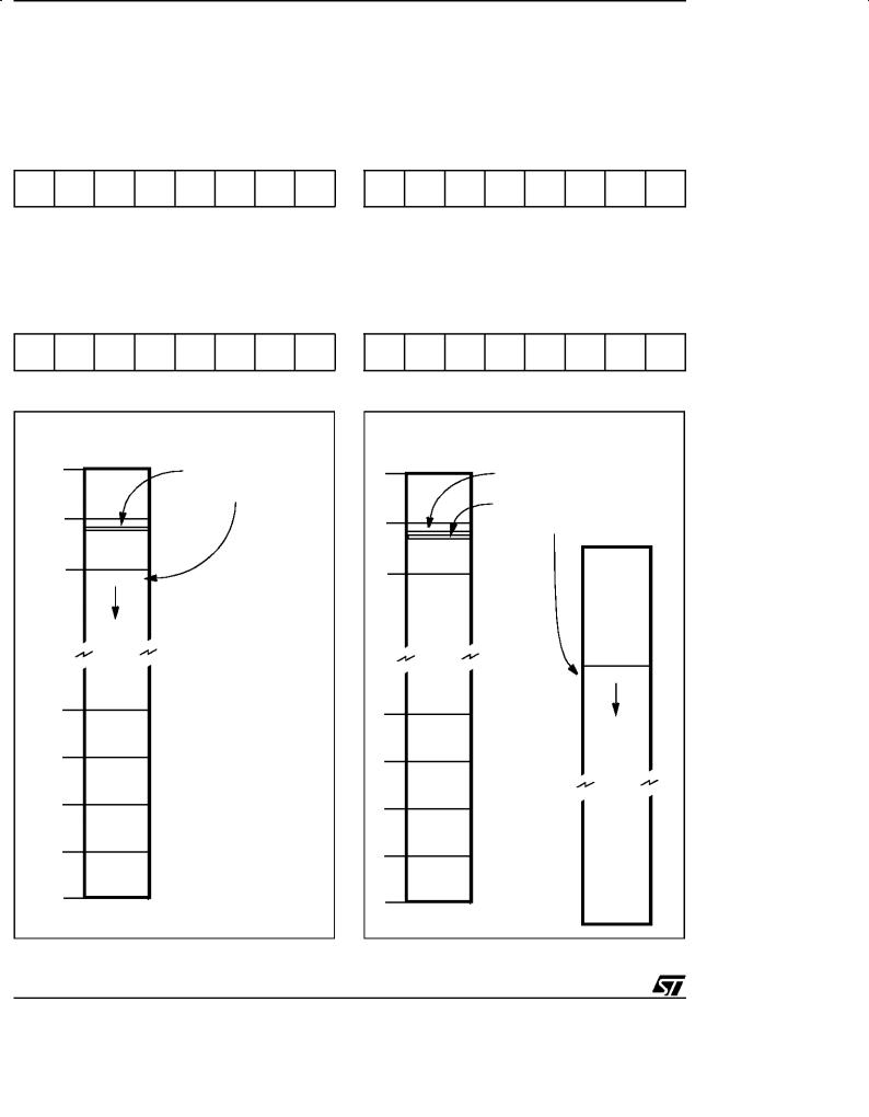
ST90158 - DEVICE ARCHITECTURE
SYSTEM REGISTERS (Cont'd)
USER STACK POINTER HIGH REGISTER (USPHR)
R236 - Read/Write Register Group: E (System) Reset value: undefined
7 |
|
|
|
|
|
0 |
USP1 USP1 USP1 USP1 USP1 USP1 |
USP9 USP8 |
|||||
5 |
4 |
3 |
2 |
1 |
0 |
|
USER STACK POINTER LOW REGISTER (USPLR)
R237 - Read/Write Register Group: E (System) Reset value: undefined
7 0
USP7 USP6 USP5 USP4 USP3 USP2 USP1 USP0
SYSTEM STACK POINTER HIGH REGISTER (SSPHR)
R238 - Read/Write Register Group: E (System) Reset value: undefined
7 |
|
|
|
|
|
0 |
SSP1 SSP1 SSP1 SSP1 SSP1 SSP1 |
SSP9 SSP8 |
|||||
5 |
4 |
3 |
2 |
1 |
0 |
|
SYSTEM STACK POINTER LOW REGISTER (SSPLR)
R239 - Read/Write Register Group: E (System) Reset value: undefined
7 |
0 |
SSP7 SSP6 SSP5 SSP4 SSP3 SSP2 SSP1 SSP0
Figure 11. Internal Stack Mode |
Figure 12. External Stack Mode |
||
|
REGIST ER |
|
REGISTER |
|
FILE |
|
|
|
|
FILE |
|
|
STACK POINTER (LOW) |
|
|
|
|
STACK POINTER (LOW) |
|
F |
points to: |
F |
& |
|
STACK POINTER (HIGH) |
||
|
|
||
|
|
|
|
|
point to: |
|
E |
MEMORY |
|
E |
||
|
||
|
STACK |
|
D |
D |
|
|
||
4 |
STACK |
|
4 |
||
|
||
3 |
3 |
|
|
||
2 |
2 |
|
|
||
1 |
1 |
|
|
||
0 |
0 |
|
|
28/190

2.4 MEMORY ORGANIZATION
Code and data are accessed within the same linear address space. All of the physically separate memory areas, including the internal ROM, internal RAM and external memory are mapped in a common address space.
The ST9+ provides a total addressable memory space of 4 Mbytes. This address space is arranged as 64 segments of 64 Kbytes; each segment is again subdivided into four 16 Kbyte pages.
ST90158 - DEVICE ARCHITECTURE
The mapping of the various memory areas (internal RAM or ROM, external memory) differs from device to device. Each 64-Kbyte physical memory segment is mapped either internally or externally; if the memory is internal and smaller than 64 Kbytes, the remaining locations in the 64-Kbyte segment are not used (reserved).
Refer to the Register and Memory Map Chapter for more details on the memory map.
29/190
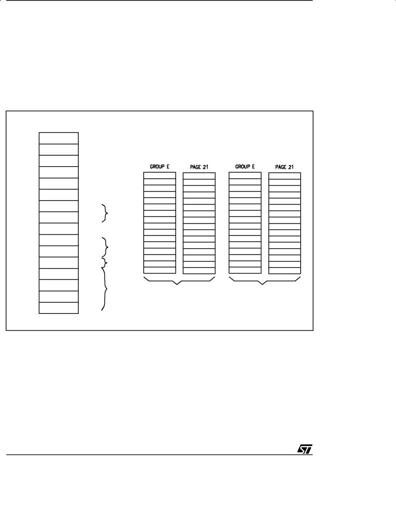
ST90158 - DEVICE ARCHITECTURE
2.5 MEMORY MANAGEMENT UNIT
The CPU Core includes a Memory Management Unit (MMU) which must be programmed to perform memory accesses (even if external memory is not used).
The MMU is controlled by 7 registers and 2 bits (ENCSR and DPRREM) present in EMR2, which may be written and read by the user program. These registers are mapped within group F, Page 21 of the Register File. The 7 registers may be
Figure 13. Page 21 Registers
sub-divided into 2 main groups: a first group of four 8-bit registers (DPR[3:0]), and a second group of three 6-bit registers (CSR, ISR, and DMASR). The first group is used to extend the address during Data Memory access (DPR[3:0]). The second is used to manage Program and Data Memory accesses during Code execution (CSR), Interrupts Service Routines (ISR or CSR), and DMA transfers (DMASR or ISR).
|
Page 21 |
|
|
|
|
|
|
|
FFh |
|
R255 |
|
|
|
|
|
|
FEh |
|
R254 |
|
Relocation of P[3:0] and DPR[3:0] Registers |
||||
|
|
|
|
|
|
|||
FDh |
|
R253 |
|
|
|
|
|
|
FCh |
|
R252 |
|
SSPLR |
|
SSPLR |
|
|
|
|
|
|
|
|
|||
FBh |
|
R251 |
|
SSPHR |
|
SSPHR |
|
|
|
|
USPLR |
|
USPLR |
|
|||
|
|
|
|
|
|
|||
FAh |
|
R250 |
|
USPHR |
|
USPHR |
|
|
F9h |
DMASR |
R249 |
|
MODER |
|
MODER |
|
|
|
PPR |
|
PPR |
|
||||
F8h |
ISR |
R248 |
MMU |
RP1 |
DMASR |
RP1 |
DMASR |
|
|
RP0 |
ISR |
RP0 |
ISR |
||||
|
|
|
|
|||||
F7h |
|
R247 |
|
FLAGR |
|
FLAGR |
|
|
|
|
CICR |
EMR2 |
CICR |
EMR2 |
|||
|
|
|
|
|||||
F6h |
EMR2 |
R246 |
|
P5DR |
EMR1 |
P5DR |
EMR1 |
|
|
|
|
EM |
P4DR |
CSR |
P4DR |
CSR |
|
F5h |
EMR1 |
R245 |
P3DR |
DPR3 |
DPR3 |
P3DR |
||
|
||||||||
F4h |
CSR |
R244 |
|
P2DR |
DPR2 |
DPR2 |
P2DR |
|
MMU |
P1DR |
1 |
DPR1 |
P1DR |
||||
F3h |
DPR3 |
R243 |
|
P0DR |
DPR0 |
DPR0 |
P0DR |
|
|
|
|
|
|
||||
F2h |
DPR2 |
R242 |
MMU |
Bit DPRREM=0 |
Bit DPRREM=1 |
|||
F1h |
DPR1 |
R241 |
||||||
|
(default setting) |
|
|
|||||
F0h |
DPR0 |
R240 |
|
|
|
|
|
|
30/190
 Loading...