


SGS Thomson Microelectronics M48T5Y-70PC1, M48T5V-70PC1, M48T59V-70MH6TR, M48T59V-70MH6, M48T59V-70MH1TR Datasheet
...M48T59
M48T59Y/M48T59V
64 Kbit (8Kb x8) TIMEKEEPER®SRAM
PRELIMINARY DATA
■INTEGRATED ULTRA LOW POWER SRAM, REAL TIME CLOCK, POWER-FAIL CONTROL CIRCUIT and BATTERY
■FREQUENCY TEST OUTPUT for REAL TIME CLOCK SOFTWARE CALIBRATION
■AUTOMATIC POWER-FAIL CHIP DESELECT and WRITE PROTECTION
■WRITE PROTECT VOLTAGES (VPFD = Power-fail Deselect Voltage):
–M48T59: 4.5V ≤ VPFD ≤ 4.75V
–M48T59Y: 4.2V ≤ VPFD ≤ 4.5V
–M48T59V: 2.7V ≤ VPFD ≤ 3.0V
■SELF-CONTAINED BATTERY and CRYSTAL in the CAPHAT DIP PACKAGE
■PACKAGING INCLUDES a 28-LEAD SOIC and SNAPHAT® TOP
(to be Ordered Separately)
■SOIC PACKAGE PROVIDES DIRECT CONNECTION for a SNAPHAT TOP which CONTAINS the BATTERY and CRYSTAL
■MICROPROCESSOR POWER-ON RESET (Valid even during battery back-up mode)
■PROGRAMMABLE ALARM OUTPUT ACTIVE in the BATTERY BACK-UP MODE
■BATTERY LOW FLAG
Table 1. Signal Names
|
A0-A12 |
Address Inputs |
|||||
|
|
|
|||||
|
DQ0-DQ7 |
Data Inputs / Outputs |
|||||
|
|
|
|
|
|
|
|
|
|
|
|
|
|
|
Interrupt / Frequency Test |
|
IRQ/FT |
||||||
|
Output (Open Drain) |
||||||
|
|
|
|
|
|
|
|
|
|
|
|
|
|
|
|
|
|
|
|
|
|
|
Power Fail Reset Output |
|
RST |
||||||
|
(Open Drain) |
||||||
|
|
|
|
|
|
|
|
|
|
|
|
|
|
||
|
|
|
|
|
Chip Enable |
||
|
E |
||||||
|
|
|
|
|
|||
|
|
|
|
|
Output Enable |
||
|
G |
||||||
|
|
|
|
||||
|
|
|
|
|
Write Enable |
||
|
W |
||||||
|
|
|
|||||
|
VCC |
Supply Voltage |
|||||
|
VSS |
Ground |
|||||
|
|
|
|
|
|
|
|
SNAPHAT (SH) |
|
|
Battery/Crytstal |
|
|
|
28 |
|
28 |
1 |
|
|
||
1 |
PCDIP28 (PC) |
|
Battery/Crystal |
||
|
||
SOH28 (MH) |
CAPHAT |
Figure 1. Logic Diagram
|
VCC |
|
13 |
|
8 |
A0-A12 |
|
DQ0-DQ7 |
W |
M48T59 |
|
|
M48T59Y |
|
E |
M48T59V |
IRQ/FT |
|
||
G |
|
RST |
VSS
AI01380E
October 1999 |
1/21 |
This is preliminary information on a new product now in development or undergoing evaluation. Details are subject to change without notice.
M48T59, M48T59Y, M48T59V
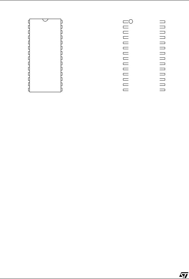
Figure 2A. DIP Connections |
|
|
|
|
|
|
|
Figure 2B. SOIC Connections |
|
|
|
|
|
|
|
|
|||||||||||
|
|
|
|
|
28 |
|
|
|
|
|
|
|
|
|
|
|
|
|
|
|
|
|
|
|
|
|
|
|
RST |
1 |
|
VCC |
|
|
RST |
1 |
|
28 |
|
VCC |
|||||||||||||||
|
A12 |
2 |
|
27 |
W |
|
|
|
|
|
A12 |
2 |
|
27 |
|
W |
|
|
|||||||||
|
A7 |
3 |
|
26 |
|
|
|
|
|
|
|
|
|
|
|
|
|
|
|
|
|
|
|
||||
|
|
IRQ/FT |
|
|
|
A7 |
3 |
|
26 |
|
|
IRQ/FT |
|||||||||||||||
|
A6 |
4 |
|
25 |
A8 |
|
|
|
A6 |
4 |
|
25 |
|
A8 |
|||||||||||||
|
A5 |
5 |
|
24 |
A9 |
|
|
|
A5 |
5 |
|
24 |
|
A9 |
|||||||||||||
|
A4 |
6 |
|
23 |
A11 |
|
|
|
A4 |
6 |
|
23 |
|
A11 |
|||||||||||||
|
A3 |
7 |
|
22 |
|
|
|
|
|
|
|
|
A3 |
7 |
M48T59Y 22 |
|
|
|
|
|
|
|
|
|
|||
|
M48T59 |
G |
|
|
|
|
|
|
|
|
|
G |
|
|
|
||||||||||||
|
A2 |
8 |
M48T59Y |
21 |
A10 |
|
|
|
A2 |
8 |
M48T59V |
21 |
|
A10 |
|||||||||||||
|
A1 |
9 |
|
20 |
E |
|
|
|
|
|
|
A1 |
9 |
|
20 |
|
|
|
|
|
|
|
|||||
|
|
|
|
|
|
|
|
|
|
E |
|||||||||||||||||
|
A0 |
10 |
|
19 |
DQ7 |
|
|
|
A0 |
10 |
|
19 |
|
DQ7 |
|||||||||||||
|
DQ0 |
11 |
|
18 |
DQ6 |
|
|
DQ0 |
11 |
|
18 |
|
DQ6 |
||||||||||||||
|
DQ1 |
12 |
|
17 |
DQ5 |
|
|
DQ1 |
12 |
|
17 |
|
DQ5 |
||||||||||||||
|
DQ2 |
13 |
|
16 |
DQ4 |
|
|
DQ2 |
13 |
|
16 |
|
DQ4 |
||||||||||||||
|
VSS |
14 |
|
15 |
DQ3 |
|
|
VSS |
14 |
|
15 |
|
DQ3 |
||||||||||||||
|
|
|
|
AI01381D |
|
|
|
|
|
|
|
|
|
|
|
AI01382E |
|
|
|
|
|
|
|
|
|||
|
|
|
|
|
|
|
|
|
|
|
|
|
|
|
|
|
|
|
|||||||||
Table 2. Absolute Maximum Ratings (1) |
|
|
|
|
|
|
|
|
|
|
|
|
|
|
|
|
|||||||||||
Symbol |
|
|
|
|
|
|
|
|
|
Parameter |
|
|
|
|
|
Value |
|
|
|
|
|
|
|
Unit |
|||
|
|
|
|
|
|
|
|
|
|
|
|
|
|
|
|
|
|
|
|
|
|
|
|
|
|
|
|
TA |
|
Ambient Operating Temperature |
|
Grade 1 |
|
0 to 70 |
|
|
|
|
|
|
|
°C |
|||||||||||||
|
|
|
|
|
|
|
|
|
|
|
|
|
|
|
|
||||||||||||
|
|
Grade 6 |
|
–40 to 85 |
|
|
|
|
|||||||||||||||||||
|
|
|
|
|
|
|
|
|
|
|
|
|
|
|
|
|
|
|
|
|
|
||||||
|
|
|
|
|
|
|
|
|
|
|
|
|
|
|
|
|
|
||||||||||
TSTG |
|
Storage Temperature (VCC Off, Oscillator Off) |
|
|
|
|
|
–40 to 85 |
|
|
|
|
|
|
|
°C |
|||||||||||
TSLD (2) |
|
Lead Solder Temperature for 10 seconds |
|
|
|
|
|
260 |
|
|
|
|
|
|
|
|
°C |
||||||||||
VIO |
|
Input or Output Voltages |
|
|
|
|
|
–0.3 to 7 |
|
|
|
|
|
|
|
V |
|||||||||||
VCC |
|
Supply Voltage |
|
|
|
|
|
|
|
|
M48T59/M48T59Y |
–0.3 to 7 |
|
|
|
|
|
|
|
V |
|||||||
|
|
|
|
|
|
|
|
|
|
|
|
|
|
|
|
|
|
|
|
|
|
|
|||||
|
|
|
|
|
|
|
|
|
M48T59V |
|
–0.3 to 4.6 |
|
|
|
|
||||||||||||
|
|
|
|
|
|
|
|
|
|
|
|
|
|
|
|
|
|
|
|
|
|
||||||
|
|
|
|
|
|
|
|
|
|
|
|
|
|
|
|
|
|
|
|
|
|
|
|
|
|
||
IO |
|
Output Current |
|
|
|
|
|
|
|
|
|
|
|
|
20 |
|
|
|
|
|
|
|
|
|
mA |
||
PD |
|
Power Dissipation |
|
|
|
|
|
|
|
|
|
|
|
|
1 |
|
|
|
|
|
|
|
|
|
W |
||
Note: 1. Stresses greater than those listed under "Absolute Maximum Ratings" may cause permanent damage to the device. This is a stress rating only and functional operation of the device at these or any other conditions above those indicated in the operational section of this specification is not implied. Exposure to the absolute maximum rating conditions for extended periods of time may affect reliability.
2. Soldering temperature not to exceed 260°C for 10 seconds (total thermal budget not to exceed 150°C for longer than 30 seconds).
CAUTION: Negative undershoots below –0.3V are not allowed on any pin while in the Battery Back-up mode. CAUTION: Do NOT wave solder SOIC to avoid damaging SNAPHAT sockets.
Table 3. Operating Modes (1)
|
VCC |
|
|
|
|
|
|
|
|
|
|
|
|
Mode |
|
E |
G |
|
W |
DQ7-DQ0 |
Power |
||||||
Deselect |
4.75V to 5.5V |
VIH |
|
X |
|
X |
High Z |
Standby |
|||||
Write |
or |
|
VIL |
|
X |
VIL |
DIN |
Active |
|||||
|
4.5V to 5.5V |
|
|
|
|
|
|
|
|
|
|
|
|
Read |
|
VIL |
VIL |
VIH |
DOUT |
Active |
|||||||
or |
|||||||||||||
Read |
3.0V to 3.6V |
|
VIL |
VIH |
VIH |
High Z |
Active |
||||||
Deselect |
VSO to VPFD (min) (2) |
|
X |
|
X |
|
X |
High Z |
CMOS Standby |
||||
Deselect |
≤ VSO |
|
X |
|
X |
|
X |
High Z |
Battery Back-up Mode |
||||
Note: 1. X = VIH or VIL; VSO = Battery Back-up Switchover Voltage. 2. See Table 7 for details.
2/21

M48T59, M48T59Y, M48T59V
Figure 3. Block Diagram
|
IRQ/FT |
|
|
OSCILLATOR AND |
16 x 8 BiPORT |
||
CLOCK CHAIN |
|||
SRAM ARRAY |
|||
|
|
||
32,768 Hz |
|
|
|
CRYSTAL |
|
A0-A12 |
|
|
|
POWER |
|
|
|
DQ0-DQ7 |
|
|
|
8176 x 8 |
|
LITHIUM |
|
SRAM ARRAY |
|
|
|
||
CELL |
|
E |
|
VOLTAGE SENSE |
W |
||
|
AND |
VPFD |
|
SWITCHING |
G |
||
CIRCUITRY |
|
||
VCC |
RST |
VSS |
|
|
|
AI01383D |
|
DESCRIPTION |
|
Table 4. AC Measurement Conditions |
|
The M48T59/59Y/59V TIMEKEEPER®RAM is an 8Kb x8 non-volatile static RAM and real time clock. The monolithic chip is available in two special packages to provide a highly integrated battery backed-up memory and real time clock solution.
The M48T59/59Y/59V is a non-volatile pin and function equivalent to any JEDEC standard 8Kb x8 SRAM. It also easily fits into many ROM, EPROM, and EEPROM sockets, providing the non-volatility of PROMs without any requirement for special write timing or limitations on the number of writes that can be performed.
The 28 pin 600mil DIP CAPHAT™ houses the M48T59/59Y/59V silicon with a quartz crystal and a long life lithium button cell in a single package.
The 28 pin 330mil SOIC provides sockets with gold plated contacts at both ends for direct connection to a separate SNAPHAT housing containing the battery and crystal. The unique design allows the SNAPHAT battery package to be mounted on top of the SOIC package after the completion of the surface mount process. Insertion of the SNAPHAT housing after reflow prevents potential battery and crystal damage due to the high temperatures required for device surfacemounting. The SNAPHAT housing is keyed to prevent reverse insertion.
Input Rise and Fall Times |
≤ 5ns |
|
|
Input Pulse Voltages |
0 to 3V |
|
|
Input and Output Timing Ref. Voltages |
1.5V |
|
|
Note that Output Hi-Z is defined as the point where data is no longer driven.
Figure 4. AC Testing Load Circuit
DEVICE 645Ω
UNDER
TEST
CL = 100pF |
|
1.75V |
|
||
|
|
CL includes JIG capacitance
AI02325
Note: Excluding open-drain output pins.
3/21

M48T59, M48T59Y, M48T59V
Table 5. Capacitance (1, 2)
(TA = 25 °C)
Symbol |
Parameter |
Test Condition |
Min |
Max |
Unit |
|
|
|
|
|
|
CIN |
Input Capacitance |
VIN = 0V |
|
10 |
pF |
|
|
|
|
|
|
CIO (3) |
Input / Output Capacitance |
VOUT = 0V |
|
10 |
pF |
Note: 1. Effective capacitance measured with power supply at 5V.
2.Sampled only, not 100% tested.
3.Outputs deselected.
Table 6. DC Characteristics
(TA = 0 to 70 °C or –40 to 85 °C; V CC = 4.75V to 5.5V or 4.5V to 5.5V or 3.0V to 3.6V)
Symbol |
|
|
Parameter |
Test Condition |
M48T59/Y |
M48T59V |
Unit |
||||||||
|
|
|
|
|
|
||||||||||
|
|
Min |
Max |
Min |
Max |
||||||||||
|
|
|
|
|
|
|
|
|
|
|
|
||||
|
|
|
|
|
|
|
|
|
|||||||
ILI (1) |
Input Leakage Current |
|
0V ≤ VIN ≤ VCC |
|
±1 |
|
±1 |
µA |
|||||||
|
|
|
|
|
|
|
|
||||||||
ILO (1) |
Output Leakage Current |
0V ≤ VOUT ≤ VCC |
|
±1 |
|
±1 |
µA |
||||||||
ICC |
Supply Current |
|
Outputs open |
|
50 |
|
30 |
mA |
|||||||
|
|
|
|
|
|
|
|
|
|
|
|
||||
ICC1 |
Supply Current (Standby) |
|
|
|
|
|
|
|
|
|
|
||||
|
|
E = VIH |
|
3 |
|
2 |
mA |
||||||||
TTL |
|
|
|
|
|||||||||||
|
|
|
|
|
|
|
|
|
|
|
|||||
|
|
|
|
|
|
|
|
|
|
|
|
||||
|
Supply Current (Standby) |
|
|
|
|
|
|
|
|
|
|
||||
ICC2 |
E = VCC – 0.2V |
|
3 |
|
1 |
mA |
|||||||||
CMOS |
|
|
|||||||||||||
|
|
|
|
|
|
|
|
|
|
|
|||||
|
|
|
|
|
|
|
|
|
|
|
|
||||
VIL (2) |
Input Low Voltage |
|
|
|
|
|
–0.3 |
0.8 |
–0.3 |
0.8 |
V |
||||
VIH |
Input High Voltage |
|
|
|
|
|
2.2 |
VCC + 0.3 |
2 |
VCC + 0.3 |
V |
||||
|
Output Low Voltage |
|
|
IOL = 2.1mA |
|
0.4 |
|
0.4 |
V |
||||||
VOL |
|
|
|
|
|
|
|
|
|
|
|
|
|||
Output Low Voltage |
|
|
|
|
|
|
|
|
|
|
|
|
|||
(IRQ/FT |
|
|
IOL = 10mA |
|
0.4 |
|
0.4 |
V |
|||||||
|
|
|
|
|
|
|
|
|
|
||||||
|
and RST) (3) |
|
|
|
|
||||||||||
|
|
|
|
|
|
|
|
|
|
|
|||||
VOH |
Output High Voltage |
|
|
IOH = –1mA |
2.4 |
|
2.4 |
|
V |
||||||
Note: 1. Outputs deselected.
2.Negative spikes of –1V allowed for up to 10ns once per cycle.
3.The IRQ/FT and RST pins are Open Drain.
Table 7. Power Down/Up Trip Points DC Characteristics (1)
(TA = 0 to 70 °C or –40 to 85 °C)
Symbol |
Parameter |
|
Min |
Typ |
Max |
Unit |
|
|
|
|
|
|
|
|
|
|
|
|
M48T59 |
4.5 |
4.6 |
4.75 |
V |
VPFD |
|
|
|
|
|
|
|
Power-fail Deselect Voltage |
M48T59Y |
4.2 |
4.35 |
4.5 |
V |
||
|
|
|
|
|
|
|
|
|
|
|
M48T59V |
2.7 |
2.9 |
3.0 |
V |
|
|
|
|
|
|
|
|
VSO |
Battery Back-up Switchover Voltage |
|
M48T59/Y |
|
3.0 |
|
V |
|
|
|
|
|
|
||
|
M48T59V |
|
VPFD –100mV |
|
V |
||
|
|
|
|
|
|||
|
|
|
|
|
|
|
|
tDR |
ExpectedDataRetentionTime(at25°C) |
|
Grade 1 |
7 |
|
|
YEARS |
|
|
|
|
|
|
||
|
Grade 6 |
10 (2) |
|
|
YEARS |
||
|
|
|
|
|
|||
Note: 1. All voltages referenced to VSS.
2. Using larger M4T32-BR12SH6 SNAPHAT top (recommended for Industrial Temperature Range - grade 6 device).
4/21
M48T59, M48T59Y, M48T59V
Table 8. Power Down/Up AC Characteristics
(TA = 0 to 70 °C or –40 to 85 °C)
Symbol |
|
|
|
|
|
|
Parameter |
Min |
Max |
Unit |
||
|
|
|
|
|
|
|
|
|
|
|||
tPD |
|
|
or |
|
at VIH before Power Down |
0 |
|
µs |
||||
E |
W |
|
||||||||||
|
|
|
|
|
|
|||||||
tF (1) |
VPFD (max) to VPFD (min) VCC Fall Time |
300 |
|
µs |
||||||||
tFB (2) |
VPFD (min) to VSS VCC Fall Time |
M48T59/Y |
10 |
|
µs |
|||||||
|
|
|
|
|||||||||
M48T59V |
150 |
|
µs |
|||||||||
|
|
|
|
|
|
|
|
|
||||
|
|
|
|
|
|
|||||||
tR |
VPFD (min) to VPFD (max) VCC Rise Time |
10 |
|
µs |
||||||||
|
|
|
|
|
||||||||
tRB |
VSS to VPFD (min) VCC Rise Time |
1 |
|
µs |
||||||||
|
|
|
|
|
|
|
|
|
|
|
|
|
(3) |
|
|
|
|
|
|
|
|
|
|
|
|
VPFD (max) to RST High |
40 |
200 |
ms |
|||||||||
tREC |
||||||||||||
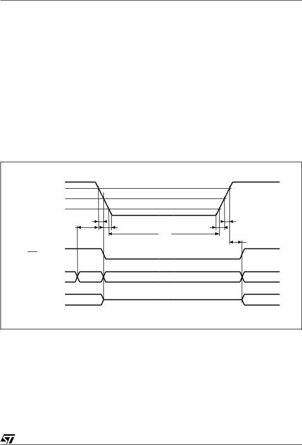
Note: 1. VPFD (max) to VPFD (min) fall time of less than tF may result in deselection/write protection not occurring until 200µs after VCC passes VPFD (min).
2.VPFD (min) to VSS fall time of less than tFB may cause corruption of RAM data.
3.tREC (min) = 20ms for industrial temperature grade 6 device.
Figure 5. Power Down/Up Mode AC Waveforms
VCC
VPFD (max)
VPFD (min) |
|
|
|
VSO |
|
|
|
|
tF |
|
tR |
tPD |
tFB |
|
tRB |
|
|
tDR |
|
|
|
|
tREC |
RST |
|
|
|
INPUTS |
RECOGNIZED |
DON'T CARE |
RECOGNIZED |
OUTPUTS |
VALID |
HIGH-Z |
VALID |
|
|||
(PER CONTROL INPUT) |
|
(PER CONTROL INPUT) |
|
|
|
|
AI03258 |
The SOIC and battery/crystal packages are shipped separately in plastic anti-static tubes or in Tape & Reel form. For the 28 lead SOIC, the battery/crystal package (i.e. SNAPHAT) part number is "M4T28-BR12SH" or “M4T32-BR12SH”.
Caution: Do not place the SNAPHAT battery/crystal top in conductive foam, as this will drain the lithium button-cell battery.
As Figure 3 shows, the static memory array and the quartz controlled clock oscillator of the M48T59/59Y/59V are integrated on one silicon chip.
The two circuits are interconnected at the upper eight memory locations to provide user accessible BYTEWIDE™ clock information in the bytes with addresses 1FF8h-1FFFh. The clock locations contain the century, year, month, date, day, hour, minute, and second in 24 hour BCD format (except for the century). Corrections for 28, 29 (leap year), 30, and 31 day months are made automatically. Byte 1FF8h is the clock control register. This byte controls user access to the clock information and also stores the clock calibration setting.
5/21
M48T59, M48T59Y, M48T59V
Table 9. Read Mode AC Characteristics
(TA = 0 to 70 °C or –40 to 85 °C; V CC = 4.75V to 5.5V or 4.5V to 5.5V or 3.0V to 3.6V)
|
|
M48T59/M48T59Y/M48T59V |
|
||
|
|
|
|
|
|
Symbol |
Parameter |
|
-70 |
Unit |
|
|
|
|
|
|
|
|
|
Min |
|
Max |
|
|
|
|
|
|
|
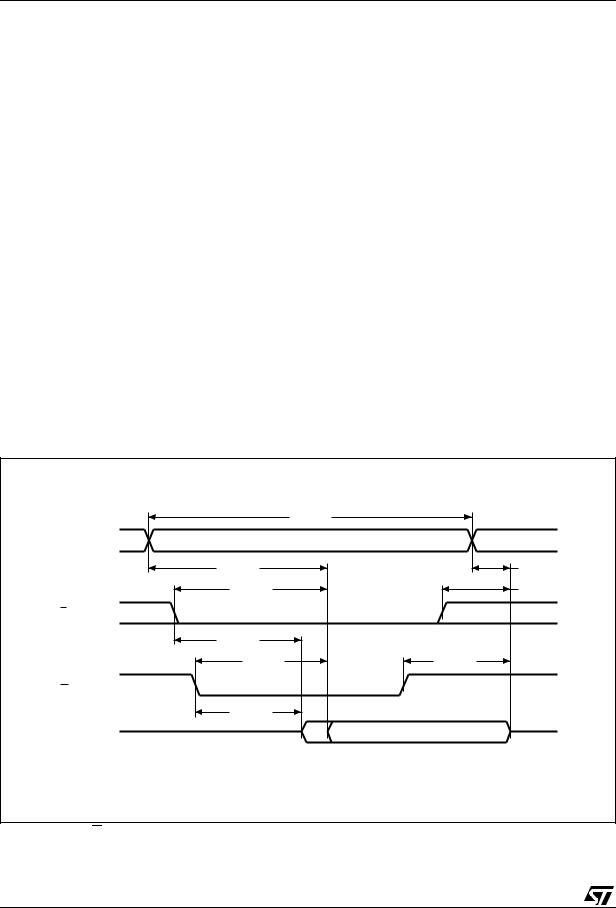
tAVAV |
Read Cycle Time |
70 |
|
|
ns |
tAVQV (1) |
Address Valid to Output Valid |
|
|
70 |
ns |
tELQV (1) |
Chip Enable Low to Output Valid |
|
|
70 |
ns |
|
|
|
|
|
|
tGLQV (1) |
Output Enable Low to Output Valid |
|
|
35 |
ns |
tELQX (2) |
Chip Enable Low to Output Transition |
5 |
|
|
ns |
tGLQX (2) |
Output Enable Low to Output Transition |
5 |
|
|
ns |
|
|
|
|
|
|
tEHQZ (2) |
Chip Enable High to Output Hi-Z |
|
|
25 |
ns |
tGHQZ (2) |
Output Enable High to Output Hi-Z |
|
|
25 |
ns |
|
|
|
|
|
|
tAXQX (1) |
Address Transition to Output Transition |
10 |
|
|
ns |
Note: 1. CL = 100pF (see Fig 4). 2. CL = 5pF (see Fig 4).
Figure 6. Read Mode AC Waveforms.
|
tAVAV |
A0-A12 |
VALID |
|
tAVQV |
|
tELQV |
E |
|
|
tELQX |
|
tGLQV |
G |
|
|
tGLQX |
DQ0-DQ7 |
|
tAXQX tEHQZ
tGHQZ
VALID
AI01385
Note: Write Enable (W) = High.
6/21

M48T59, M48T59Y, M48T59V
Table 10. Write Mode AC Characteristics
(TA = 0 to 70 °C or –40 to 85 °C; V CC = 4.75V to 5.5V or 4.5V to 5.5V or 3.0V to 3.6V)
|
|
|
M48T59/M48T59Y/M48T59V |
|
||
|
|
|
|
|
|
|
Symbol |
Parameter |
|
-70 |
Unit |
||
|
|
|
|
|
|
|
|
|
|
Min |
|
Max |
|
|
|
|
|
|
|
|
tAVAV |
Write Cycle Time |
70 |
|
|
ns |
|
tAVWL |
Address Valid to Write Enable Low |
0 |
|
|
ns |
|
|
|
|
|
|
|
|
tAVEL |
Address Valid to Chip Enable Low |
0 |
|
|
ns |
|
|
|
|
|
|
|
|
tWLWH |
Write Enable Pulse Width |
50 |
|
|
ns |
|
tELEH |
Chip Enable Low to Chip Enable High |
55 |
|
|
ns |
|
|
|
|
|
|
|
|
tWHAX |
Write Enable High to Address Transition |
0 |
|
|
ns |
|
|
|
|
|
|
|
|
tEHAX |
Chip Enable High to Address Transition |
0 |
|
|
ns |
|
tDVWH |
Input Valid to Write Enable High |
30 |
|
|
ns |
|
|
|
|
|
|
|
|
tDVEH |
Input Valid to Chip Enable High |
30 |
|
|
ns |
|
|
|
|
|
|
|
|
tWHDX |
Write Enable High to Input Transition |
5 |
|
|
ns |
|
tEHDX |
Chip Enable High to Input Transition |
5 |
|
|
ns |
|
|
|
|
|
|
|
|
tWLQZ (1, 2) |
Write Enable Low to Output Hi-Z |
|
|
25 |
ns |
|
|
|
|
|
|
|
|
tAVWH |
Address Valid to Write Enable High |
60 |
|
|
ns |
|
tAVE1H |
Address Valid to Chip Enable High |
60 |
|
|
ns |
|
tWHQX (1, 2) |
Write Enable High to Output Transition |
5 |
|
|
ns |
|
Note: 1. CL = 5pF (see Fig 4).
2. If E goes low simultaneously with W going low, the outputs remain in the high impedance state.
The eight clock bytes are not the actual clock counters themselves; they are memory locations consisting of BiPORT™ read/write memory cells. The M48T59/59Y/59V includes a clock control circuit which updates the clock bytes with current information once per second. The information can be accessed by the user in the same manner as any other location in the static memory array.
The M48T59/59Y/59V also has its own Power-fail Detect circuit. The control circuitry constantly monitors the single 5V supply for an out of tolerance condition. When VCC is out of tolerance, the circuit write protects the SRAM, providing a high degree of data security in the midst of unpredictable system operation brought on by low VCC. As VCC falls below approximately 3V, the control circuitry connects the battery which maintains data and clock operation until valid power returns.
READ MODE
The M48T59/59Y/59V is in the Read Mode whenever W (Write Enable) is high and E (Chip Enable) is low. The unique address specified by the 13 Address Inputs defines which one of the 8,192 bytes of data is to be accessed. Valid data will be available at the Data I/O pins within Address Access time (tAVQV) after the last address input signal is
stable, providing that the E and G access times are also satisfied. If the E and G access times are not met, valid data will be available after the latter
of the Chip Enable Access time (tELQV) or Output Enable Access time (tGLQV).
The state of the eight three-state Data I/O signals is controlled by E and G. If the outputs are activat-
ed before tAVQV, the data lines will be driven to an indeterminate state until tAVQV. If the Address In-
puts are changed while E and G remain active, output data will remain valid for Output Data Hold
time (tAXQX) but will go indeterminate until the next Address Access.
7/21
 Loading...