


ST72F63BK2B1
SGS Thomson Microelectronics ST72F63BK2B1, ST72F63BK2, ST72F63BK1M1, ST72F63BK1, ST72F63BK1B1 Datasheet
...
Rev. 1.5
April 2003 1/132
ST7263B
LOW SPEED USB 8-BIT MCU FAMILY WITH FLASH/ROM,
UP TO 512 BYTES RAM, 8-BIT ADC, WDG , TIMER, SCI
& I²C
■ Memories
– 4, 8 or 16 Kbytes Program Memory: High
Density Flash (HDFlash) or ROM with Read-
out and Write Protection
– In-Application Programming (IAP) and In-Cir-
cuit programming (ICP) for HDFlash devices
– 384 or 512 bytes RAM memory (128-byte
stack)
■ Clock , Res et and Supp ly M a nagemen t
– Run, Wait, Slow and Halt CPU modes
– 12 or 24 MHz Oscillator
– RAM Retention mode
– Optional Low Voltage Detector (LVD)
■ USB (Universal Serial Bus) Interface
– DMA for low speed applications compliant
with USB 1.5 Mbs (version 1.1) and HID spec-
ifications (version 1.0)
– Integrated 3.3 V voltage regulator and trans-
ceivers
– Suspend and Resume operations
– 3 Endpoints with programmable In/Out config-
uration
■ 19 I/O Ports
– 8 high sink I/Os (10 mA at 1.3 V)
– 2 very high sink true open drain I/Os (25 mA
at 1.5 V)
– 8 lines individually programmable as interrupt
inputs
■ 2 Timers
– Programmable Watchdog
– 16-bit Timer with 2 Input Captures, 2 Ou tput
Compares, PWM output and clock input
■ 2 Communication Interfaces
– Asynchronous Serial Communications Inter-
face (on K4 and K2 versions only)
– I²C Multi Master Interface up to 400 kHz
(on K4 versions only)
■ 1 Analog Peripheral
– 8-bit A/D Converter (ADC) with 8 channels
■ Instruction Set
– 63 basic instruction s
– 17 main addressing modes
– 8 x 8 unsigned multiply instruction
– True bit manipulation
■ Development Tools
– Versatile Development Tools (under Win-
dows) including assem bler, linker, C-compil-
er, archiver, source level debugger, software
library, hardware emulator, programming
boards and gang programmers
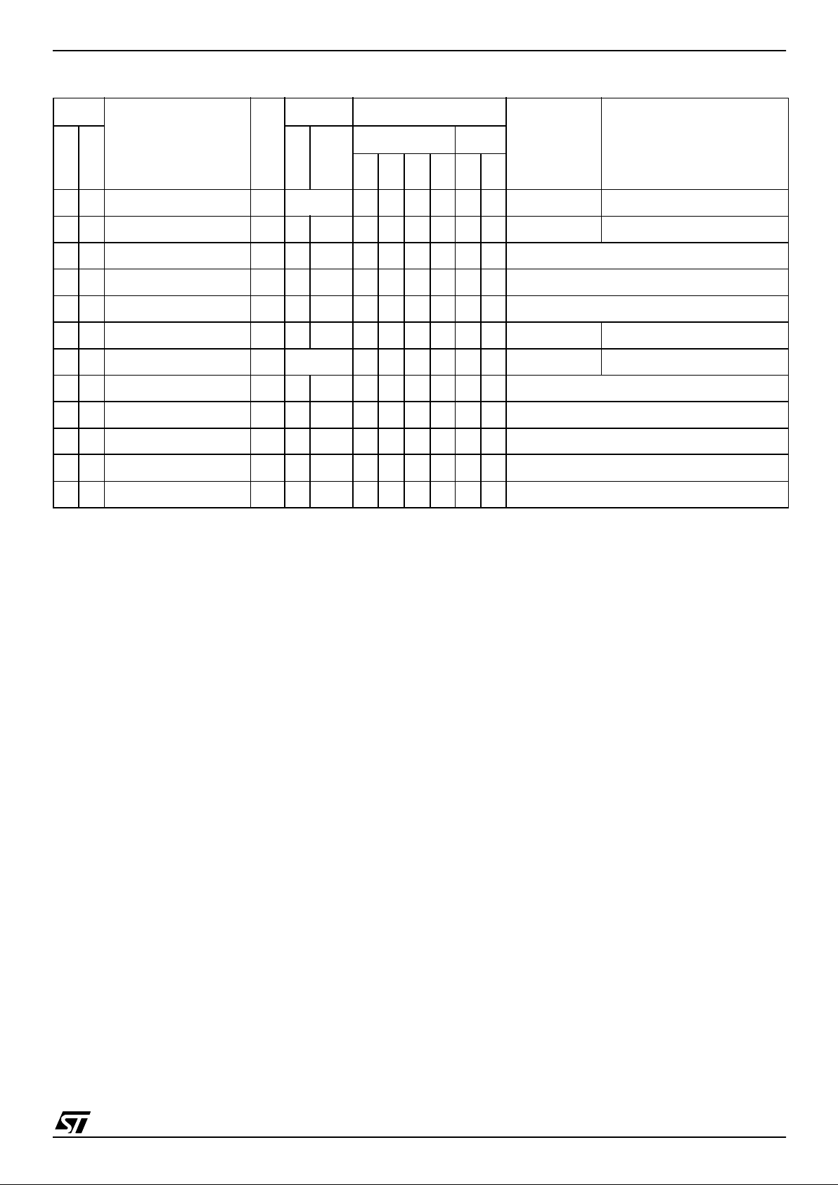
Table 1. Device Summa ry
SO34 (Shrink)
PSDIP32
Features
ST72F63BK4
ST7263BK2 ST7263BK1
Program Memory -bytes-
16K
(Flash or FASTROM)
8K
(Flash, ROM or FASTROM)
4K
(Flash, ROM or FASTROM)
RAM (stack) - bytes 512 (128) 384 (128)
Peripherals
Watchdog timer, 16-bit tim-
er, SCI, I²C, ADC, USB
Watchdog timer,
16-bit timer, SCI, ADC, USB
Watchdog, 16-bit timer, ADC,
USB
Operating Supply 4.0 V to 5.5 V
CPU frequency 8 MHz (with 24 MHz oscillator) or 4 MHz (with 12 MHz oscillator)
Operating temperature 0 °C to +70 °C
Packages SO34/SDIP32
1

Table of Cont ents
132
2/132
1 INTRODUCTION . . . . . . . . . . . . . . . . . . . . . . . . . . . . . . . . . . . . . . . . . . . . . . . . . . . . . . . . . . . . . . 4
2 PIN DESCRIPTION . . . . . . . . . . . . . . . . . . . . . . . . . . . . . . . . . . . . . . . . . . . . . . . . . . . . . . . . . . . . 5
3 REGISTER & MEMORY MAP . . . . . . . . . . . . . . . . . . . . . . . . . . . . . . . . . . . . . . . . . . . . . . . . . . . . 8
4 FLASH PROGRAM MEMORY . . . . . . . . . . . . . . . . . . . . . . . . . . . . . . . . . . . . . . . . . . . . . . . . . . 11
4.1 INTRODUCTION . . . . . . . . . . . . . . . . . . . . . . . . . . . . . . . . . . . . . . . . . . . . . . . . . . . . . . . . 11
4.2 MAIN FEATURES . . . . . . . . . . . . . . . . . . . . . . . . . . . . . . . . . . . . . . . . . . . . . . . . . . . . . . . 11
4.3 STRUCTURE . . . . . . . . . . . . . . . . . . . . . . . . . . . . . . . . . . . . . . . . . . . . . . . . . . . . . . . . . . . 11
4.4 ICC INTERFACE . . . . . . . . . . . . . . . . . . . . . . . . . . . . . . . . . . . . . . . . . . . . . . . . . . . . . . . . 12
4.5 ICP (IN-CIRCUIT PROGRAMMING) . . . . . . . . . . . . . . . . . . . . . . . . . . . . . . . . . . . . . . . . . 13
4.6 IAP (IN-APPLICATION PROGRAMMING) . . . . . . . . . . . . . . . . . . . . . . . . . . . . . . . . . . . . . 13
5 CENTRAL PROCESSING UNIT . . . . . . . . . . . . . . . . . . . . . . . . . . . . . . . . . . . . . . . . . . . . . . . . . 14
5.1 INTRODUCTION . . . . . . . . . . . . . . . . . . . . . . . . . . . . . . . . . . . . . . . . . . . . . . . . . . . . . . . . 14
5.2 MAIN FEATURES . . . . . . . . . . . . . . . . . . . . . . . . . . . . . . . . . . . . . . . . . . . . . . . . . . . . . . . 14
5.3 CPU REGISTERS . . . . . . . . . . . . . . . . . . . . . . . . . . . . . . . . . . . . . . . . . . . . . . . . . . . . . . . 14
6 RESET AND CLOCK MANAGEMENT . . . . . . . . . . . . . . . . . . . . . . . . . . . . . . . . . . . . . . . . . . . . 17
6.1 RESET . . . . . . . . . . . . . . . . . . . . . . . . . . . . . . . . . . . . . . . . . . . . . . . . . . . . . . . . . . . . . . . . 17
6.2 CLOCK SYSTEM . . . . . . . . . . . . . . . . . . . . . . . . . . . . . . . . . . . . . . . . . . . . . . . . . . . . . . . . 19
7 INTERRUPTS . . . . . . . . . . . . . . . . . . . . . . . . . . . . . . . . . . . . . . . . . . . . . . . . . . . . . . . . . . . . . . . 20
7.1 INTERRUPT REGISTER . . . . . . . . . . . . . . . . . . . . . . . . . . . . . . . . . . . . . . . . . . . . . . . . . . 22
8 POWER SAVING MODES . . . . . . . . . . . . . . . . . . . . . . . . . . . . . . . . . . . . . . . . . . . . . . . . . . . . . 23
8.1 INTRODUCTION . . . . . . . . . . . . . . . . . . . . . . . . . . . . . . . . . . . . . . . . . . . . . . . . . . . . . . . . 23
8.2 HALT MODE . . . . . . . . . . . . . . . . . . . . . . . . . . . . . . . . . . . . . . . . . . . . . . . . . . . . . . . . . . . 23
8.3 SLOW MODE . . . . . . . . . . . . . . . . . . . . . . . . . . . . . . . . . . . . . . . . . . . . . . . . . . . . . . . . . . . 24
8.4 WAIT MODE . . . . . . . . . . . . . . . . . . . . . . . . . . . . . . . . . . . . . . . . . . . . . . . . . . . . . . . . . . . 24
9 I/O PORTS . . . . . . . . . . . . . . . . . . . . . . . . . . . . . . . . . . . . . . . . . . . . . . . . . . . . . . . . . . . . . . . . . . 25
9.1 INTRODUCTION . . . . . . . . . . . . . . . . . . . . . . . . . . . . . . . . . . . . . . . . . . . . . . . . . . . . . . . . 25
9.2 FUNCTIONAL DESCRIPTION . . . . . . . . . . . . . . . . . . . . . . . . . . . . . . . . . . . . . . . . . . . . . . 25
9.3 I/O PORT IMPLEMENTATION . . . . . . . . . . . . . . . . . . . . . . . . . . . . . . . . . . . . . . . . . . . . . . 26
10 MISCELLANEOUS REGISTER . . . . . . . . . . . . . . . . . . . . . . . . . . . . . . . . . . . . . . . . . . . . . . . . 32
11 ON-CHIP PERIPHERALS . . . . . . . . . . . . . . . . . . . . . . . . . . . . . . . . . . . . . . . . . . . . . . . . . . . . . 33
11.1WATCHDOG TIMER (WDG) . . . . . . . . . . . . . . . . . . . . . . . . . . . . . . . . . . . . . . . . . . . . . . . 33
11.216-BIT TIMER . . . . . . . . . . . . . . . . . . . . . . . . . . . . . . . . . . . . . . . . . . . . . . . . . . . . . . . . . . 36
11.3SERIAL COMMUNICATIONS INTERFACE (SCI) . . . . . . . . . . . . . . . . . . . . . . . . . . . . . . . 55
11.4USB INTERFACE (USB) . . . . . . . . . . . . . . . . . . . . . . . . . . . . . . . . . . . . . . . . . . . . . . . . . . 67
11.5I²C BUS INTERFACE (I²C) . . . . . . . . . . . . . . . . . . . . . . . . . . . . . . . . . . . . . . . . . . . . . . . . . 75
11.68-BIT A/D CONVERTER (ADC) . . . . . . . . . . . . . . . . . . . . . . . . . . . . . . . . . . . . . . . . . . . . . 86
12 INSTRUCTION SET . . . . . . . . . . . . . . . . . . . . . . . . . . . . . . . . . . . . . . . . . . . . . . . . . . . . . . . . . 90
12.1ST7 ADDRESSING MODES . . . . . . . . . . . . . . . . . . . . . . . . . . . . . . . . . . . . . . . . . . . . . . . 90
12.2INSTRUCTION GROUPS . . . . . . . . . . . . . . . . . . . . . . . . . . . . . . . . . . . . . . . . . . . . . . . . . 93
13 ELECTRICAL CHARACTERISTICS . . . . . . . . . . . . . . . . . . . . . . . . . . . . . . . . . . . . . . . . . . . . . 96
13.1PARAMETER CONDITIONS . . . . . . . . . . . . . . . . . . . . . . . . . . . . . . . . . . . . . . . . . . . . . . . 96
13.2ABSOLUTE MAXIMUM RATINGS . . . . . . . . . . . . . . . . . . . . . . . . . . . . . . . . . . . . . . . . . . . 97

Table of Cont ents
3/132
13.3OPERATING CONDITIONS . . . . . . . . . . . . . . . . . . . . . . . . . . . . . . . . . . . . . . . . . . . . . . . . 98
13.4SUPPLY CURRENT CHARACTERISTICS . . . . . . . . . . . . . . . . . . . . . . . . . . . . . . . . . . . 100
13.5CLOCK AND TIMING CHARACTERISTICS . . . . . . . . . . . . . . . . . . . . . . . . . . . . . . . . . . 101
13.6MEMORY CHARACTERISTICS . . . . . . . . . . . . . . . . . . . . . . . . . . . . . . . . . . . . . . . . . . . 103
13.7EMC CHARACTERISTICS . . . . . . . . . . . . . . . . . . . . . . . . . . . . . . . . . . . . . . . . . . . . . . . 104
13.8I/O PORT PI N CHARACTERISTICS . . . . . . . . . . . . . . . . . . . . . . . . . . . . . . . . . . . . . . . . 109
13.9CONTROL PIN CHARACTERISTICS . . . . . . . . . . . . . . . . . . . . . . . . . . . . . . . . . . . . . . . 114
13.10COMMUNICATION INTERFACE CHARACTERISTICS . . . . . . . . . . . . . . . . . . . . . . . . 116
13.118-BIT ADC CHARACTERISTICS . . . . . . . . . . . . . . . . . . . . . . . . . . . . . . . . . . . . . . . . . . 119
14 PACKAGE CHARACTERISTICS . . . . . . . . . . . . . . . . . . . . . . . . . . . . . . . . . . . . . . . . . . . . . . 121
14.1PACKAGE MECHANICAL DATA . . . . . . . . . . . . . . . . . . . . . . . . . . . . . . . . . . . . . . . . . . . 121
14.2THERMAL CHARACTERISTICS . . . . . . . . . . . . . . . . . . . . . . . . . . . . . . . . . . . . . . . . . . 122
14.3SOLDERING AND GLUEABILITY INFORMATION . . . . . . . . . . . . . . . . . . . . . . . . . . . . . 123
15 DEVICE CONFIGURATION AND ORDERING INFORMATION . . . . . . . . . . . . . . . . . . . . . . . 124
15.1OPTION BYTE . . . . . . . . . . . . . . . . . . . . . . . . . . . . . . . . . . . . . . . . . . . . . . . . . . . . . . . . . 124
15.2DEVICE ORDERING INFORMATION . . . . . . . . . . . . . . . . . . . . . . . . . . . . . . . . . . . . . . . 125
15.3DEVELOPMENT TOOLS . . . . . . . . . . . . . . . . . . . . . . . . . . . . . . . . . . . . . . . . . . . . . . . . . 126
15.4ST7 APPLICATION NOTES . . . . . . . . . . . . . . . . . . . . . . . . . . . . . . . . . . . . . . . . . . . . . . 128
16 KNOWN LIMITATIONS . . . . . . . . . . . . . . . . . . . . . . . . . . . . . . . . . . . . . . . . . . . . . . . . . . . . . . 130
16.1UNEXPECTED RESET FETCH . . . . . . . . . . . . . . . . . . . . . . . . . . . . . . . . . . . . . . . . . . . . 130
16.2HALT MODE POWER CONSUMPTION WITH ADC ON . . . . . . . . . . . . . . . . . . . . . . . . . 130
17 SUMMARY OF CHANGES . . . . . . . . . . . . . . . . . . . . . . . . . . . . . . . . . . . . . . . . . . . . . . . . . . . 131
To obtain the most recent version of this datasheet,
please check at www.st.com>products>technical literature>datasheet
Please also pay special attention to the Section “IMPORTANT NOTES” on page 130.
ST7263B
4/132
1 INTRODUCTION
The ST7263B Microcontrollers form a sub-family
of the ST7 MCUs dedicated to USB applications.
The devices are based on an industry-standard 8-
bit core and feature an enhanced instruction set.
They operate at a 24 MHz or 12 MHz oscillator fre-
quency. Under software control, the ST7263B
MCUs may be placed in either Wait or Halt modes,
thus reducing power consumption. The enhan ced
instruction set an d addressing modes afford real
programming potential. In addi tion to standard 8-
bit data management, the ST7263B MCUs feature
true bit manipulation, 8x8 unsigned multiplica tion
and indirect addressing modes. The devices in-
clude an ST7 Core, up to 16 Kbytes of program
memory, up to 512 bytes of RAM, 19 I/O lines and
the following on-chip peripherals:
– USB low speed interface with 3 endpoints with
programmable in/out configuration using the
DMA architecture with embedded 3.3V voltage
regulator and transceivers (no external compo-
nents are needed).
– 8-bit Analog-to-Digital converter (ADC) with 8
multiplexed analog inputs
– Industry standard asynchronous SCI serial inter-
face (not on all products - see Table 1 Device
Summary)
– Watc hdog
– 16-bit Timer featuring an External clock input, 2
Input Captures, 2 Output Compares with Pulse
Generator capab ilities
– Fast I²C Multi Master interface (not on all prod-
ucts - see device summary)
– Low voltage reset (LVD) ensuring proper power-
on or power-off of the device
The ST7263B devices are ROM versions.
The ST72P63B devices are Factory Advanced
Service Technique ROM (FASTROM) versions:
they are factory-programmed and are not repro-
grammable.
The ST72F63B d evices are Flash versions. They
support programming in IAP mode (In-application
programming) via the on-chip USB interface.
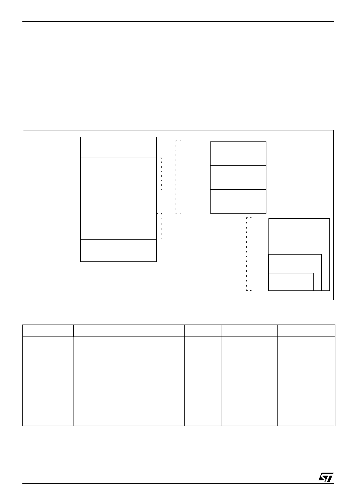
Figure 1. General Block Diagram
8-BIT CO RE
ALU
ADDRESS AND DATA BUS
OSCIN
OSCOUT
RESET
PORT B
16-B IT TIMER
PORT A
PORT C
PB[7:0]
(8 bits)
PC[2:0]
(3 bits)
OSCILLATOR
INTERNAL
CLOCK
CONTROL
RAM
(384/512 Bytes)
PA[7:0]
(8 bits)
V
SS
V
DD
POWER
SUPPLY
SCI*
PROGRAM
(4K/8K/16K Byte s)
I²C*
MEMORY
ADC
(UART)
USB SIE
OSC/3
LVD
WATCHDOG
V
SSA
V
DDA
V
PP
/TEST
USB DMA
USBDP
USBDM
USBVCC
OSC/4 or OSC/2
(for USB)
* Not on all products (refer to Ta bl e 1: Device S ummary )
ST7263B
5/132
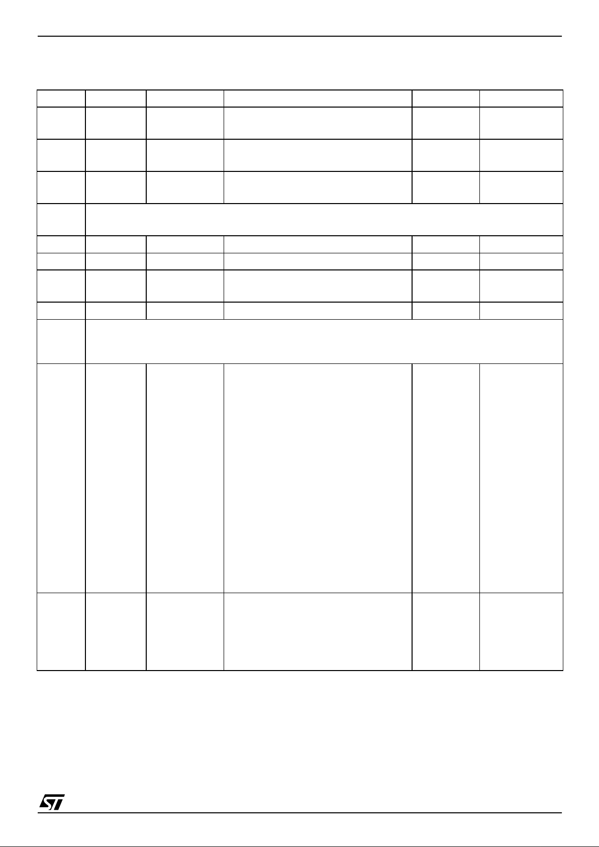
2 PIN DESCRIPTION
Figure 2. 34-Pin SO Package Pinout
Figure 3. 32-Pin SDIP Package Pinout
18
19
20
21
22
23
31
30
29
28
27
26
25
24
1
2
3
4
5
6
7
8
9
10
11
12
13
14
V
DD
OSCOUT
AIN4/IT5/PB4
(10mA)
AIN5/IT6/PB5
(10mA)
V
PP
/TEST
AIN6/PB6/IT7
(10mA)
AIN7/IT 8PB7
(10mA)
NC
RESET
PC0/RDI
PC1/TDO
PC2/USBOE
V
SS
OSCIN
USBDP
V
SSA
PB0
(10mA)
/AIN0
PA7/OCMP2/IT4
PA6/OCMP1/IT3
PA5/ICAP2/IT2
PA4/ICAP1/IT1
PA3/EXTCLK
PA2
(25mA)
/SCL/ICCCLK
NC
NC
NC
PA1
(25mA)
/SDA/ICCDATA
PA0/MCO
15
16
17
AIN1/PB1
(10mA)
AIN2/PB2
(10mA)
AIN3/PB3
(10mA)
34
33
32
V
DDA
USBVCC
USBDM
* V
PP
on Flash versions only
28
27
26
25
24
23
22
21
20
19
18
17
16
15
1
2
3
4
5
6
7
8
9
10
11
12
13
14
29
30
31
32
V
DD
OSCOUT
AIN1/PB1/
(10mA)
AIN2/PB2
(10mA)
AIN3/PB3
(10mA)
AIN4/IT5/PB4
(10mA)
AIN5/IT6/PB5
(10mA)
V
PP
/TEST*
AIN6/IT7/PB6
(10mA)
PC0/RDI
PC1/TDO
PC2/USBOE
V
SS
OSCIN
AIN7/IT8/PB7
(10mA)
RESET
V
DDA
USBVCC
PB0
(10mA)
/AIN0
PA7/COMP2/IT4
PA6/COMP1/IT3
PA5/ICAP2/IT2
PA4/ICAP1/IT1
PA3/EXTCLK
PA2
(25mA)
/SCL/ICCCLK
PA1
(25mA)
/SDA/ICCDATA
PA0/MCO
V
SSA
USBDP
USBDM
NC
NC
* V
PP
on Flash versions only
ST7263B
6/132
PIN DESCRIPTION (Cont’d)
RESET
(see Note 1): Bidirectional. This active l ow
signal forces the initialization of the MCU. This
event is the top priority non maskable interrupt.
This pin is switched low when the Watchdog is trig-
gered or the V
DD
is low. It can be used t o reset ex-
ternal peripherals.
OSCIN/OSCOUT: Input/Output Oscillator pin.
These pins connect a pa rallel-resonant cryst al, or
an external source, to the on-chip oscillator.
V
DD
/V
SS
(see Note 2): Main Power Supply and
Ground voltages.
V
DDA
/V
SSA
(see Note 2): Power Supply and
Ground voltages for analog peripherals.
Alter n at e Fu nct i on s: Several pins of the I/O ports
assume software programmable alternate func-
tions as shown in the pin description.
Note 1: Adding two 100 nF decou pling capacitors
on the Reset pin (respectively connected to
V
DD
and V
SS
) will significantly improve produ ct electro-
magnetic susceptibility performance.
Note 2: To enhance the reliability of operation, it is
recommended that
V
DDA
and V
DD
be connected to-
gether on the appl ication board. This also applies
to
V
SSA
and V
SS
.
Table 2. Device Pin Description
Pin n°
Pin Name
Type
Level Port / Control
Main
Function
(after reset)
Alternate Function
SDIP32
SO34
Input
Output
Input Output
float
wpu
int
ana
OD
PP
11V
DD
S Power supply voltage (4V - 5.5V)
2 2 OSCOUT O Oscillator output
3 3 OSCIN I Oscillator input
44V
SS
S Digital ground
5 5 PC2/USBOE I/O C
T
X X Port C2 USB Output Enable
6 6 PC1/TDO I/O C
T
X X Port C1 SCI Transmit Data Output*
7 7 PC0/RDI I/O C
T
X X Port C0 SCI Receive Data Input*
8 8 RESET I/O X X Reset
-- 9 NC -- Not connected
9 10 PB7/AIN7/IT8 I/O C
T
10mA X XX XPort B7 ADC analog input 7
10 11 PB6/AIN6/IT7 I/O C
T
10mA X XX XPort B6 ADC analog input 6
11 12 V
PP
/TEST S Programming supply
12 13 PB5/AIN5/IT6 I/O C
T
10mA X XX XPort B5 ADC analog input 5
13 14 PB4/AIN4/IT5 I/O C
T
10mA X XX XPort B4 ADC analog input 4
14 15 PB3/AIN3 I/O C
T
10mA X XXPort B3 ADC analog input 3
15 16 PB2/AIN2 I/O C
T
10mA X XXPort B2 ADC analog input 2
16 17 PB1/AIN1 I/O C
T
10mA X XXPort B1 ADC analog input 1
17 18 PB0/AIN0 I/O C
T
10mA X XXPort B0 ADC Analog Input 0
18 19 PA7/OCMP2/IT4 I/O C
T
X XXPort A7 Timer Output Compare 2
19 20 PA6/OCMP1/IT3 I/O C
T
X XXPort A6 Timer Output Compare 1
20 21 PA5/ICAP2/IT2 I/O C
T
X XXPort A5 Timer Input Captu re 2
21 22 PA4/ICAP 1/IT1 I/O C
T
X XXPort A4 Timer Input Captu re 1
ST7263B
7/132
Note (*): if the peripheral is present on the device (see Table 1, "Device Summary")
Legend / Abbreviations for Figure 2 and Table 2 :
Type: I = input, O = output, S = supply
In/Output le v el: C
T
= CMOS 0.3V
DD
/0.7V
DD
with input trigger
Output level: 10mA = 10mA high sink (on N-buffer only)
25mA = 25mA very high sink (on N-buffer only)
Port and control configuration:
– Input: float = floating, wpu = weak pull-up, int = interrupt, ana = analog
– Out put: OD = open drain, PP = push-pull, T = True open drain
Refer to “I/O PORTS” on page 25 for more details on the software configuration of the I/O ports.
The RESET co n fi g u ra tion of each p i n is shown in bold. This configuration is kept as long as the device is
under reset state.
22 23 PA3/EXTCLK I/O C
T
X X Port A3 Timer External Clock
23 24 PA2/SCL/ ICCC LK I/O C
T
25mA X T Port A2 I²C serial clock*, ICC Clock
-- 25 NC -- Not connected
24 26 NC -- Not connected
25 27 NC -- Not connected
26 28 PA1/SDA/ICCDATA I/O C
T
25mA X T Port A1 I²C serial data*, ICC Data
27 29 PA0/MCO I/O C
T
XXPort A0 Main Clock Output
28 30 V
SSA
S Analog ground
29 31 USBDP I/O USB bidirectional data (data +)
30 32 USBDM I/O USB bidirectional data (data -)
31 33 USBVCC O USB power supply
32 34 V
DDA
S Analog supply voltage
Pin n°
Pin Name
Type
Level Port / Control
Main
Function
(after reset)
Alternate Function
SDIP32
SO34
Input
Output
Input Output
float
wpu
int
ana
OD
PP
ST7263B
8/132
3 REGISTER & MEMORY MAP
As sho wn i n Figure 4, the MCU is capable of ad-
dressing 64 Kbytes of memories and I/O registers.
The available memory locations consist of up to
512 bytes of RAM including 64 bytes of register lo-
cations, and up to 16K bytes of user program
memory in which the upper 32 bytes are reserved
for interrupt vectors. The RAM space includes up
to 128 bytes for the stack from 0100h to 017Fh.
The highest address bytes contain the user re set
and interrupt vectors.
IMPORTANT: Memory locations noted “Re-
served” must ne ver be accessed. Ac cessing a re-
served area can have unpredictable effects on the
device.
Figure 4. Me m ory M a p
* Program memory and RAM sizes are product dependent (see Table 1, " Device Summary")
Table 3. Interrupt Vector Map
Vector Address Description Masked by Remarks Exit from Halt Mode
FFE0h-FFEDh
FFEEh-FFEFh
FFF0h-FFF1h
FFF2h-FFF3h
FFF4h-FFF5h
FFF6h-FFF7h
FFF8h-FFF9h
FFFAh-FFFBh
FFFCh-FFFDh
FFFEh-FFFFh
Reserved Area
USB Interrupt Vector
SCI Interrupt Vector
I²C Interrupt Vector
TIMER Interrupt Vector
IT1 to IT8 Interrupt Vector
USB End Suspend Mode Interrupt Vector
Flash Start Programming Interrupt Vector
TRAP (software) Interrupt Vector
RESET Vector
I- bit
I- bit
I- bit
I- bit
I- bit
I- bit
I- bit
None
None
Internal Interrupt
Internal Interrupt
Internal Interrupt
Internal Interrupt
External Interrupt
External Interrupts
Internal Interrupt
CPU Interrupt
No
No
No
No
Yes
Yes
Yes
No
Yes
0000h
RAM
Program Memory*
(4/8/16 KBytes)
Interrupt & Reset Vectors
HW Registers
0040h
003Fh
FFDFh
FFE0h
FFFFh
Reserved
Stack
(128 Bytes)
0100h
017Fh
01BF/023Fh
01C0/0240h
00FFh
0040h
0180h
01BF/023Fh
Short Addressing
RAM (192 bytes)
16-bit Addressing
RAM
C000h
BFFFh
(See Table 4)
(See Table 3)
(384/512 Bytes)
FFDFh
C000h
F000h
E000h
4 KBytes
8 KBytes
16 KBytes
ST7263B
9/132
Table 4. Hardware Regist er Memo ry Ma p
Address Block Register Label Register name Reset Status Remarks
0000h
0001h
Port A
PADR
PADDR
Port A Data Register
Port A Data Direction Register
00h
00h
R/W
R/W
0002h
0003h
Port B
PBDR
PBDDR
Port B Data Register
Port B Data Direction Register
00h
00h
R/W
R/W
0004h
0005h
Port C
PCDR
PCDDR
Port C Data Register
Port C Data Direction Register
1111 x000b
1111 x000b
R/W
R/W
0006h
0007h
Reserved (2 Bytes)
0008h ITC ITIFRE Interrupt Register 00h R/W
0009h MISC MISCR Miscellaneous Register 00h R/W
000Ah
000Bh
ADC
ADCDR
ADCCSR
ADC Data Register
ADC control Status register
00h
00h
Read only
R/W
000Ch WDG WDGCR Watchdog Control Register 7Fh R/W
000Dh
to
0010h
Reserved (4 bytes)
0011h
0012h
0013h
0014h
0015h
0016h
0017h
0018h
0019h
001Ah
001Bh
001Ch
001Dh
001Eh
001Fh
TIM
TCR2
TCR1
TSR
TIC1HR
TIC1LR
TOC1HR
TOC1LR
TCHR
TCLR
TACHR
TACLR
TIC2HR
TIC2LR
TOC2HR
TOC2LR
Timer Control Register 2
Timer Control Register 1
Timer Status Register
Timer Input Capture High Register 1
Timer Input Capture Low Register 1
Timer Output Compare High Register 1
Timer Output Compare Low Register 1
Timer Counter High Register
Timer Counter Low Register
Timer Alternate Counter High Register
Timer Alternate Counter Low Register
Timer Input Capture High Register 2
Timer Input Capture Low Register 2
Timer Output Compare High Register 2
Timer Output Compare Low Register 2
00h
00h
00h
xxh
xxh
80h
00h
FFh
FCh
FFh
FCh
xxh
xxh
80h
00h
R/W
R/W
Read only
Read only
Read only
R/W
R/W
Read only
R/W
Read only
R/W
Read only
Read only
R/W
R/W
0020h
0021h
0022h
0023h
0024h
SCI
1)
SCISR
SCIDR
SCIBRR
SCICR1
SCICR2
SCI Status Register
SCI Data Register
SCI Baud Rate Register
SCI Control Register 1
SCI Control Register 2
C0h
xxh
00h
x000 0000b
00h
Read only
R/W
R/W
R/W
R/W
ST7263B
10/132
Note 1. If the peripheral is present on the device (see Table 1, "Device Summary")
0025h
0026h
0027h
0028h
0029h
002Ah
002Bh
002Ch
002Dh
002Eh
002Fh
0030h
0031h
USB
USBPIDR
USBDMAR
USBIDR
USBISTR
USBIMR
USBCTLR
USBDADDR
USBEP0RA
USBEP0RB
USBEP1RA
USBEP1RB
USBEP2RA
USBEP2RB
USB PID Register
USB DMA address Register
USB Interrupt/DMA Register
USB Interrupt Status Register
USB Interrupt Mask Register
USB Control Register
USB Device Address Register
USB Endpoint 0 Register A
USB Endpoint 0 Register B
USB Endpoint 1 Register A
USB Endpoint 1 Register B
USB Endpoint 2 Register A
USB Endpoint 2 Register B
x0h
xxh
x0h
00h
00h
06h
00h
0000 xxxxb
80h
0000 xxxxb
0000 xxxxb
0000 xxxxb
0000 xxxxb
Read only
R/W
R/W
R/W
R/W
R/W
R/W
R/W
R/W
R/W
R/W
R/W
R/W
0032h to
0036h
Reserved (5 bytes)
0032h
0036h
Reserved (5 Bytes)
0037h Flash FCSR Flash Control /Status Register 00h R/W
0038h Reserved (1 byte)
0039h
003Ah
003Bh
003Ch
003Dh
003Eh
003Fh
I²C
1)
I2CDR
I2COAR
I2CCCR
I2CSR2
I2CSR1
I2CCR
I²C Data Register
Reserved
I²C (7 Bits) Slave Address Register
I²C Clock Control Register
I²C 2nd Status Register
I²C 1st Status Register
I²C Control Register
00h
-
00h
00h
00h
00h
00h
R/W
R/W
R/W
Read only
Read only
R/W
Address Block Register Label Register name Reset Status Remarks
ST7263B
11/132
4 FLASH PROGRAM MEMO RY
4.1 Introduction
The ST7 dual voltage High Density Flash
(HDFlash) is a non-volatile memory that can be
electrically erased as a single block or by individu-
al sectors and programmed on a Byte-by-Byte ba-
sis using an external V
PP
supply.
The HDFlash devices can be programmed and
erased off-board (plugge d in a programm ing tool)
or on-board using ICP (In-Circuit Programming) or
IAP (In-Application Programming).
The array matrix organ isation allows each sector
to be erased and reprogramm ed without affecting
other sectors.
4.2 Main Features
■ Three Flash programming modes :
– Insertion in a programming tool. In this m ode,
all sectors including option bytes can be pro-
grammed or erased.
– ICP (In-Circuit Programming). In this mode, all
sectors including option bytes can be pro-
grammed or erased without removing the de-
vice from the application board.
– IAP (In-Application Programming) In this
mode, all sectors except Sector 0, can be pro-
grammed or erased without removing the de-
vice from the application board a nd wh ile the
application is running.
■ ICT (In-Circuit Testing) for downloading and
executing user application test patterns in RAM
■ Read-out protection against piracy
■ Register Access Security System (RASS) to
prevent accidental programming or erasing
4. 3 S tructure
The Flash memory is organised in sectors and can
be used for both code and data storage.
Depending on the overall Flash memory size in the
microcontroller device, there are up to three user
sectors (see Ta ble 5). Each of these sectors can
be erased independently to avoid unnecessary
erasing of the whole Flas h memory when only a
partial erasing is required.
The first two sectors have a fixed siz e of 4 Kby tes
(see Figure 5). They are mapped in the upper part
of the ST7 addressing space so t he reset and in-
terrupt vectors are located in Sector 0 (F000h-
FFFFh).
Table 5. Sectors available in Flash devices
4.3.1 Read-out Protection
Read-out protection, when s elected, makes it im-
possible to extract the memory content from the
microcontroller, thus preventing piracy. Even ST
cannot access the user code.
In flash devices, this protection is removed by re-
programming the option. In this case, the entire
program memory is first automatically erased.
Read-out protection selection depend s on the de-
vice type:
– In Flash devices it is enabled and removed
through the FMP_R bit in the option byte.
– In ROM devices it is enabled by mask option
specified in the Option List.
Figure 5. Me m ory M a p and Sector A dd re ss
Flash Size (bytes) Available Sectors
4K Sector 0
8K Sectors 0,1
> 8K Sectors 0,1, 2
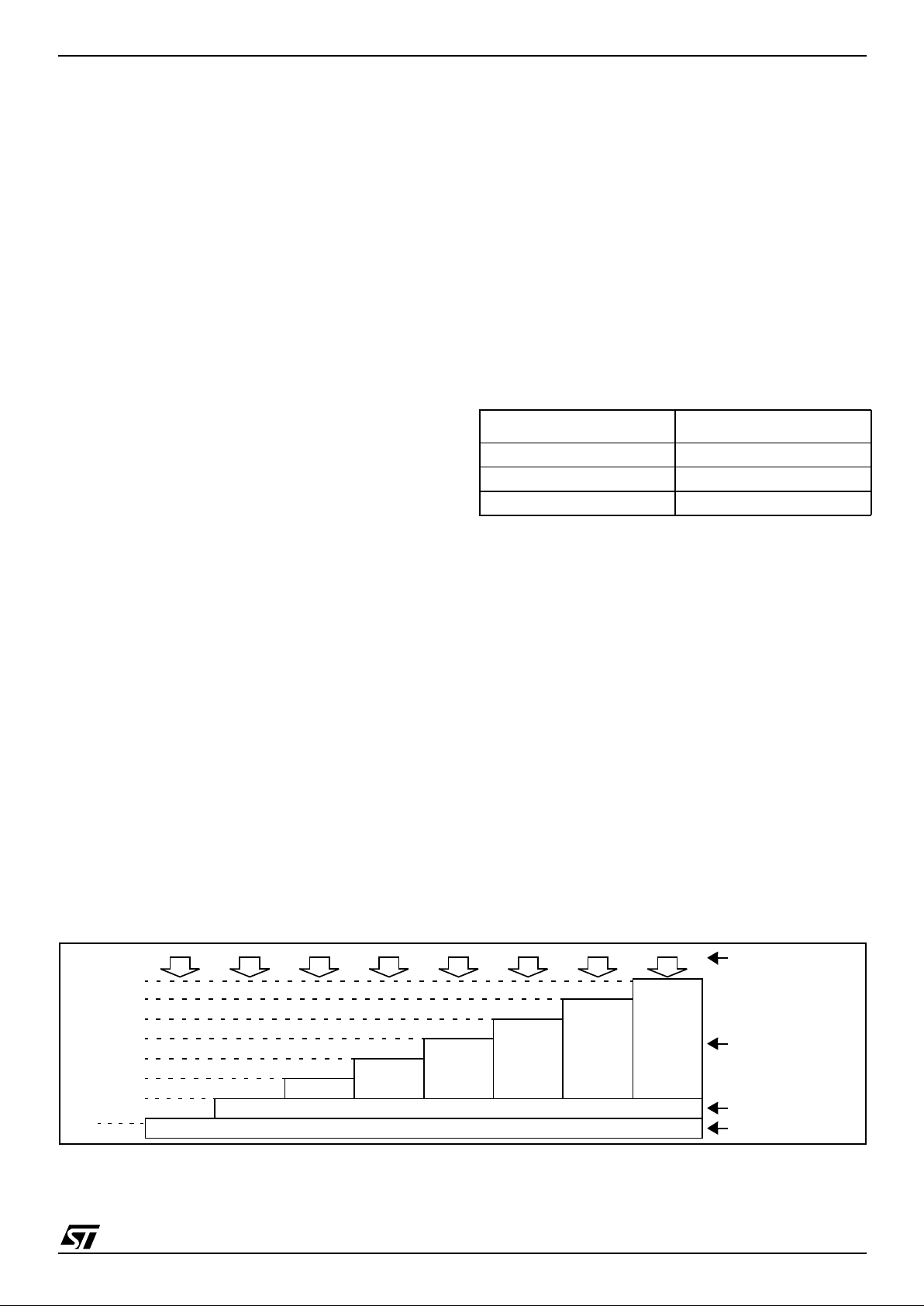
4 Kbytes
4 Kbytes
2Kbytes
SECTOR 1
SECTOR 0
16 Kbytes
SECTOR 2
8K 16K 32K 60K
FLASH
FFFFh
EFFFh
DFFFh
3FFFh
7FFFh
1000h
24 Kbytes
MEMORY SIZE
8Kbytes 40 Kbytes
52 Kby t es
9FFFh
BFFFh
D7FFh
4K 10K 24K 48K
ST7263B
12/132
FLASH PROGRAM MEMORY (Cont’d)
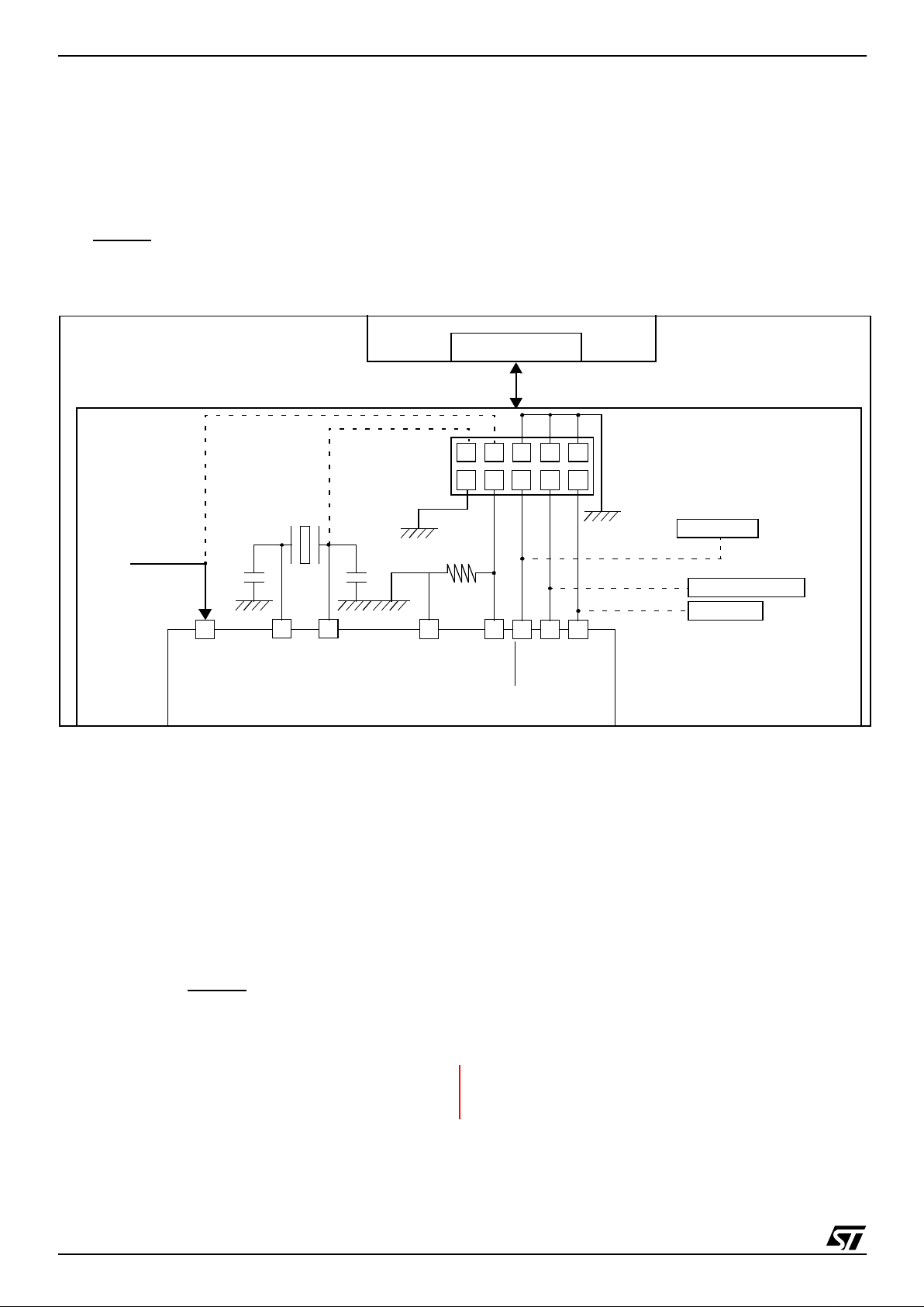
4.4 ICC Interface
ICC needs a m inimum of 4 and up to 6 pins to b e
connected to the programming tool (see Figure 6).
These pins are:
– RESET
: device reset
–V
SS
: device power supply ground
– ICCCLK: ICC output serial clock pin
– ICCDATA: ICC input/output serial data pin
– ICCSEL/V
PP
: programming voltage
– OSC1(or OSCIN): main clock input for exter-
nal source (optional)
–V
DD
: application board power su pply (option-
al, see Figure 6, Note 3)
Figure 6. Typical ICC Interface
Notes:
1. If the ICCCLK or ICCDATA pins are only u sed
as outputs in t he ap plication, n o s ign al iso lation is
necessary. As soon as the Programming Tool is
plugged to the board, even if an ICC session is not
in progress, the ICCCLK and ICCDATA pins are
not available for the application. If they are used as
inputs by the application, isolation such as a serial
resistor has to implemented in case another de-
vice forces the signal. Refer to the Programming
Tool documentation for recommended resistor val-
ues.
2. During the ICC session, the programming tool
must control the RESET
pin. This can lead to con-
flicts between the programming tool and the appli-
cation reset circuit if it drives more than 5mA at
high level (push pull output or pull-up resistor<1K).
A schottky diode can be us ed to iso late the appli-
cation RESET circuit in this case. When using a
classical RC network with R>1K or a reset man-
agement IC with open drain output and pull-up re-
sistor>1K, no additional com ponents are needed.
In all cases the user must ensure that no external
reset is generated by the application during the
ICC session.
3. The use of Pin 7 of the ICC con nector de pends
on the Programming Tool architecture. This pin
must be connected when using most ST Program-
ming Tools (it is used to monitor the application
power supply). Please refer to the Programming
Tool manual.
4. Pin 9 has to be co nnected to the OS C1 or OS-
CIN pin of the ST7 when the clock is not available
in the application or if the sel ected clock opt ion is
not programmed in t he option byte. ST7 devices
with multi-oscillator capability need to have OSC2
grounded in this case.
5. During normal operation, the ICCCLK pin must
be pulled-up, internally or externally, to avoid en-
tering ICC mode unexpectedly during a reset.
ICC CONNECTOR
ICCDATA
ICCCLK
RESET
V
DD
HE10 CONNECTOR TYPE
APPLICATION
POWER SUPPLY
1
246810
975 3
PROGRAMMING TOOL
ICC CONNECTOR
APPLICATION BOARD
ICC Cab le
OPTIONAL
(See No te 3)
10k
Ω
V
SS
ICCSEL/VPP
ST7
C
L2
C
L1
OSC1
OSC2
OPTIONAL
See Note 1
See No tes 1 and 5
See Note 2
APPLICATION
RESET SOURCE
APPLICATI ON
I/O
(See No te 4)

ST7263B
13/132
FLASH PROGRAM MEMORY (Cont’d)
4.5 ICP (In-Circuit Programming)
To perform ICP the microcontroller must be
switched to ICC (In-Circuit Communication) mode
by an external controller or programming tool.
Depending on the ICP code dow nloaded in RAM,
Flash memory programming can be fully custom-
ized (number of bytes to prog ram, program loca-
tions, or selection serial communication interface
for downloading).
When using an STMicroelectronics or third-party
programming tool that supp orts ICP and the spe-
cific microcontroller device, the user needs only to
implement the ICP hardware interface on the ap-
plication board (see Figure 6). For more details on
the pin locations, refer to the device pinout de-
scription.
4.6 IA P ( I n-Application P rogramming )
This mode uses a BootLoader program previously
stored in Sector 0 by the us er (in ICP mode or by
plugging the device in a programming tool).
This mode is fully controlled by user software. This
allows it to be adapted to the user application, (us-
er-defined strategy for entering programming
mode, choice of communications protocol us ed to
fetch the data to be stored, etc.). For example, it is
possible to download code from the SPI, SCI, USB
or CAN interface and program it in the Flash. IAP
mode can be used to program any of the Flash
sectors except Sector 0, whi ch is write/erase pro-
tected to allow recovery in case errors occur dur-
ing the programming operation.
4.6.1 Register Description
FLASH CONTROL/STATUS REGISTER (FCSR)
Read/Write
Reset Value: 0000 0000 (00h)
This register is reserved for use by Programming
Tool software. It controls the Flash programming
and erasing operations. For details on customizing
Flash programming methods and In-Circuit T est-
ing, refer to the ST7 Flash Programming Refer-
ence Manual.
70
00000000
ST7263B
14/132
5 CENTRAL PROCE SSING UNIT
5.1 INTRODUCTION
This CPU has a full 8-bit architecture and contains
six internal registers allowing efficient 8-bit data
manipulation.
5.2 MAIN FEATURES
■ 63 basic instructions
■ Fast 8-bit by 8-bit multiply
■ 17 main addressing modes
■ Two 8-bit index registers
■ 16-bit stack pointer
■ Low po wer m odes
■ Maskable hardware interrupts
■ Non-maskable software interrupt
5.3 CPU REGISTERS
The 6 CPU registers shown in Figure 7 are not
present in the memory mapping and are accessed
by specific instructions.
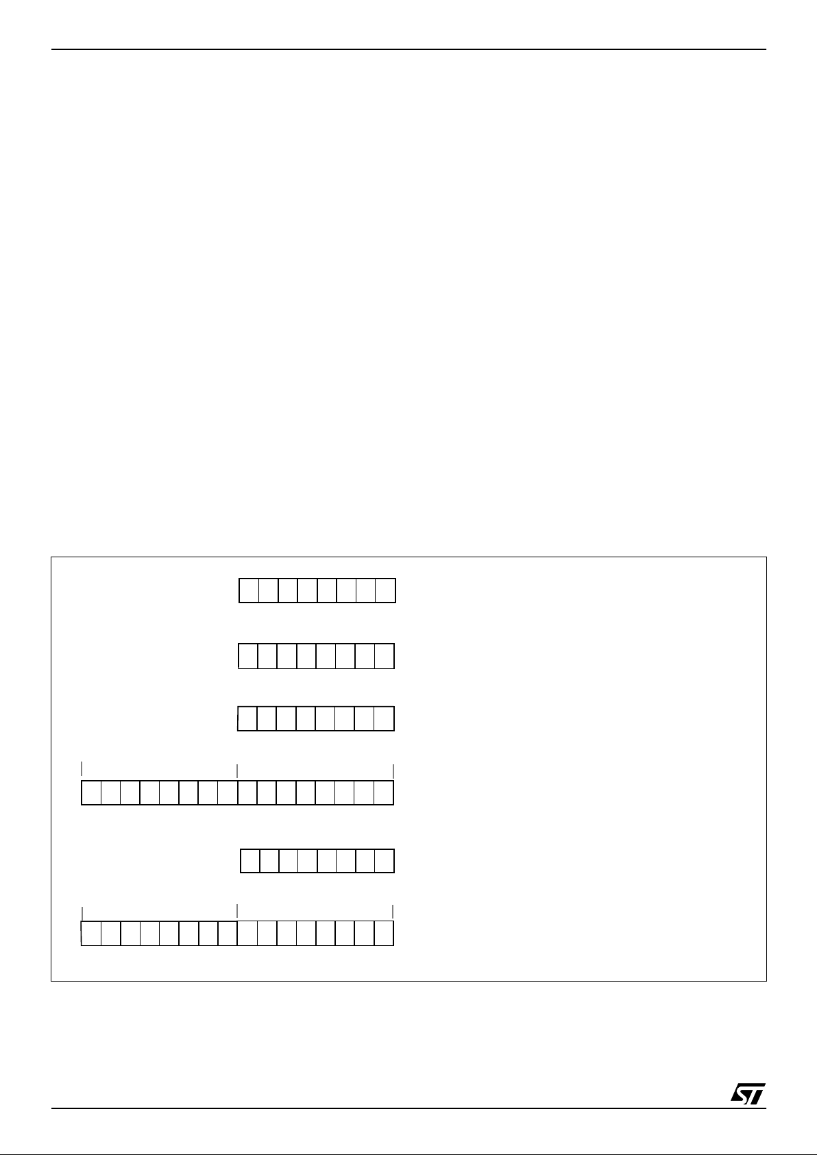
Accumulator (A)
The Accumulator is an 8-bit general purpose reg-
ister used to hold operands and the res ults of the
arithmetic and logic calculations and to manipulate
data.
Index Registers (X and Y)
In indexed addressing modes, these 8-bit registers
are used to create either effective addresses or
temporary storage areas for data manipulation.
(The Cross-Assembler generates a precede in-
struction (PRE) to indicate that the following in-
struction refers to the Y register.)
The Y register is not affected by the interrupt auto-
matic procedures (not pushed to and popped from
the stack).
Program Counter (PC)
The program counter is a 16-bit register containing
the address of the next instruction to be executed
by the CPU. It is made of two 8-bit registers PCL
(Program Counter Low which is the LSB) and PCH
(Program Counter High which is the MSB).
Figure 7. CPU Registers
ACCUMULATOR
X INDEX REGISTER
Y INDEX REGISTER
STACK POINTER
CONDITION CODE REGISTER
PROGRAM COUNTER
70
1C11HI NZ
RESET VALUE = RESET VECTOR @ FFFEh-FFFFh
70
70
70
0
7
15 8
PCH
PCL
15
8
70
RESET VALUE = STACK HIGHER ADDRESS
RESET VALUE =
1X11X1XX
RESET VALUE = XXh
RESET VALUE = XXh
RESET VALUE = XXh
X = Undefined Value

ST7263B
15/132
CPU REGISTERS (Cont’d)
CONDITION CODE REGISTER (CC)
Read/Write
Reset Value: 111x1xxx
The 8-bit Condition Code regist er contains the i n-
terrupt mask and four flags repres entative of the
result of the instruction just executed. This register
can also be handled by the PUSH and POP in-
structions.
These bits can be individually tested and/or con-
trolled by specific instructions.
Bit 4 = H
Half carry
.
This bit is set by hardware when a carry occurs be-
tween bits 3 and 4 of t he ALU during an ADD or
ADC instruction. It is reset by hardware during the
same instructi ons.
0: No half carry has occurred.
1: A half carry has occurred.
This bit is tested using the JRH or JRNH instruc-
tion. The H bit is useful in BCD arithmetic subrou-
tine s .
Bit 3 = I
Interrupt mask
.
This bit is set by hardware when entering in inter-
rupt or by software to disable all inte rrupts except
the TRAP software interrupt. This bit is cleared by
software.
0: Interrupts are enabled.
1: Interrupts are disabled.
This bit is controlled by the RIM, SIM and IRET in-
structions and is tested by the JRM and JR NM in-
structions.
Note: Interrupts requested while I is set are
latched and can be process ed when I is cleared.
By default an interrupt routine is not in terruptable
because the I bi t is set by h ardware at the start of
the routine and reset by the IRET instruction at the
end of the routine. If the I bit is cleared by software
in the interrupt routine, pending interrupts are
serviced regardless of the priority level of the cur-
rent interrupt routine.
Bit 2 = N
Negative
.
This bit is set and cleared by hardware. It is repre-
sentative of the result sign of the last arithm etic,
logical or data manipulation. It is a copy of the 7
th
bit of the result.
0: The result of the last operation is positive or null.
1: The result of the last operation is negative
(i.e. the most significant bit is a logic 1).
This bit is accessed by the JRMI and JRPL instruc-
tions.
Bit 1 = Z
Zero
.
This bit is set and cleared by hardware. This bit in-
dicates that the result of the last arithmetic, logical
or data manipulation is zero.
0: The result of the last operation is different from
zero.
1: The result of the last operation is zero.
This bit is accessed by the JREQ and JRNE test
instructions.
Bit 0 = C
Carry/borrow.
This bit is set and cleared b y hardware and soft-
ware. It indicates an overflow or an un derflow has
occurred during the last arithmetic operation.
0: No overflow or underflow has occurred.
1: An overflow or underflow has occurred.
This bit is driven by the SCF and RCF instructions
and tested by the JRC and JRNC instructions. It i s
also affected by the “bit test and branch”, shift and
rotate instructions.
70
111HINZC
ST7263B
16/132
CPU REGISTERS (Cont’d)
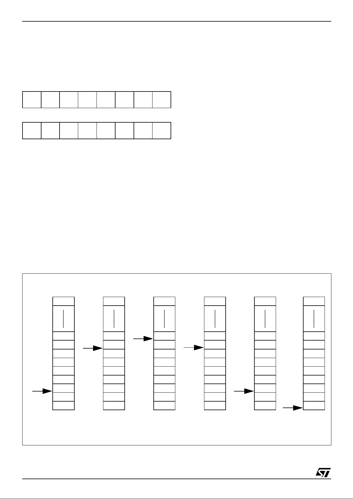
STACK POINTER (SP)
Read/Write
Reset Value: 017Fh
The Stack Pointer is a 16-bit register which is al-
ways pointing to the next free location in the stack.
It is then decremented after data has been pushed
onto the stack and incremented before data is
popped from the stack (see Figure 8).
Since the stack is 128 bytes deep, the 9 most sig-
nificant bits are forced by hard ware. Following a n
MCU Reset, or after a Reset Stack Pointer instruc-
tion (RSP), the Stack Pointer contains its reset val-
ue (the SP6 to SP0 bits are set) which is the stack
higher address.
The least significant byte of the Stack Pointer
(called S) can be directly accessed by a LD in-
struction.
Note: When the lower limit is exceeded, the Stack
Pointer wraps around to the stack upper limit, with-
out indicating the stack overflow. The previously
stored information is then o verwritten and there-
fore lost. The stack also wraps in case of an under-
flow.
The stack is used to sav e the return address dur-
ing a subroutine call and the CPU context during
an interrupt. The user may also directly manipulate
the stack by means of the PUSH and POP instruc-
tions. In the case of an interrupt, the PCL is stored
at the first location po inted t o by t he SP. Th en t he
other registers are stored in the next locations as
shown in Figure 8.
– When an interrupt is received, the SP is decre-
mented and the context is pushed on the stack.
– On return from interrupt, the SP is incremented
and the context is popped from the stack.
A subroutine call occupies two locations and an in-
terrupt five locat ion s i n the stack ar ea.
Figure 8. Stack Manipulation Example
15 8
00000001
70
0 SP6 SP5 SP4 SP3 SP2 SP1 SP0
PCH
PCL
SP
PCH
PCL
SP
PCL
PCH
X
A
CC
PCH
PCL
SP
PCL
PCH
X
A
CC
PCH
PCL
SP
PCL
PCH
X
A
CC
PCH
PCL
SP
SP
Y
CALL
Subroutine
Interrupt
Event
PUSH Y POP Y IRET
RET
or RSP
@ 017Fh
@ 0100h
Stack Higher Address = 017Fh
Stack Lower Address =
0100h
ST7263B
17/132
6 RESET AND CLOCK MANAGEMENT
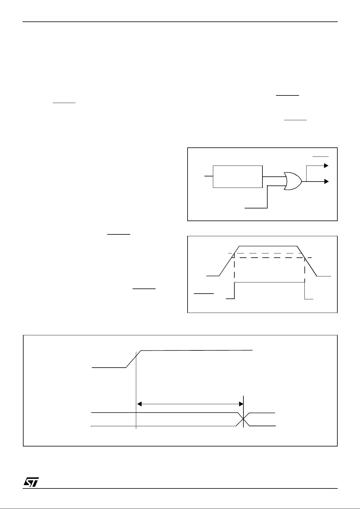
6.1 RESET
The Reset procedure is used to provide an orderly
software start-up or to exit low power modes.
Three reset modes are provided: a low voltage
(LVD) reset, a watchdog rese t and an external re-
set at the RESET
pin.
A reset causes the reset vector to be fetched from
addresses FFFEh and FFFFh in order to be loaded
into the PC and with program execution starting
from this point.
An internal circuitry provides a 4096 CPU clock cy-
cle delay from the time that the oscillator becomes
active.
6.1.1 Low Voltage Detector (LVD)
Low voltage reset circuitry generates a reset when
V
DD
is:
■ below V
IT+
when V
DD
is rising,
■ below V
IT-
when V
DD
is falling.
During low voltage reset, the RESET
pin is held low,
thus permitting the MCU to reset other devices.
The Low Voltage Detector can be disabled by set-
ting bit 3 of the option byte.
6.1.2 Watchdog Reset
When a watchdo g reset occ urs, t he RESET
pin is
pulled low permitting the MCU to reset other devic-
es in the same way as the low voltage reset (Fi g-
ure 9).
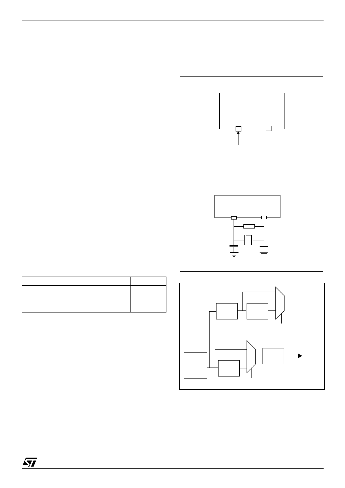
6.1.3 External Reset
The external reset is an active low input signal ap-
plied to the RESET pin of the MCU.
As shown in Figure 12, the RESET
signal must
stay low for a minimum of one and a half CPU
clock cycles.
An internal Schmitt trigger at the RESET
pin is pro-
vided to improve noise immunity.
Figure 9. Low Voltage Detector functional Diagram
Figure 10. Low Voltage Reset Signal Output
Note: Hysteresis (V
IT+
-V
IT-
) = V
hys
Figure 11. Temporization timing diagram after an internal Reset
LOW VOLTAGE
V
DD
FROM
WATCHDOG
RESET
RESET
INTERNAL
DETECTOR
RESET
RESET
V
DD
V
IT+
V
IT-
V
DD
Addresses
$FFFE
Temporization (4096 CPU clock cycles)
V
IT+
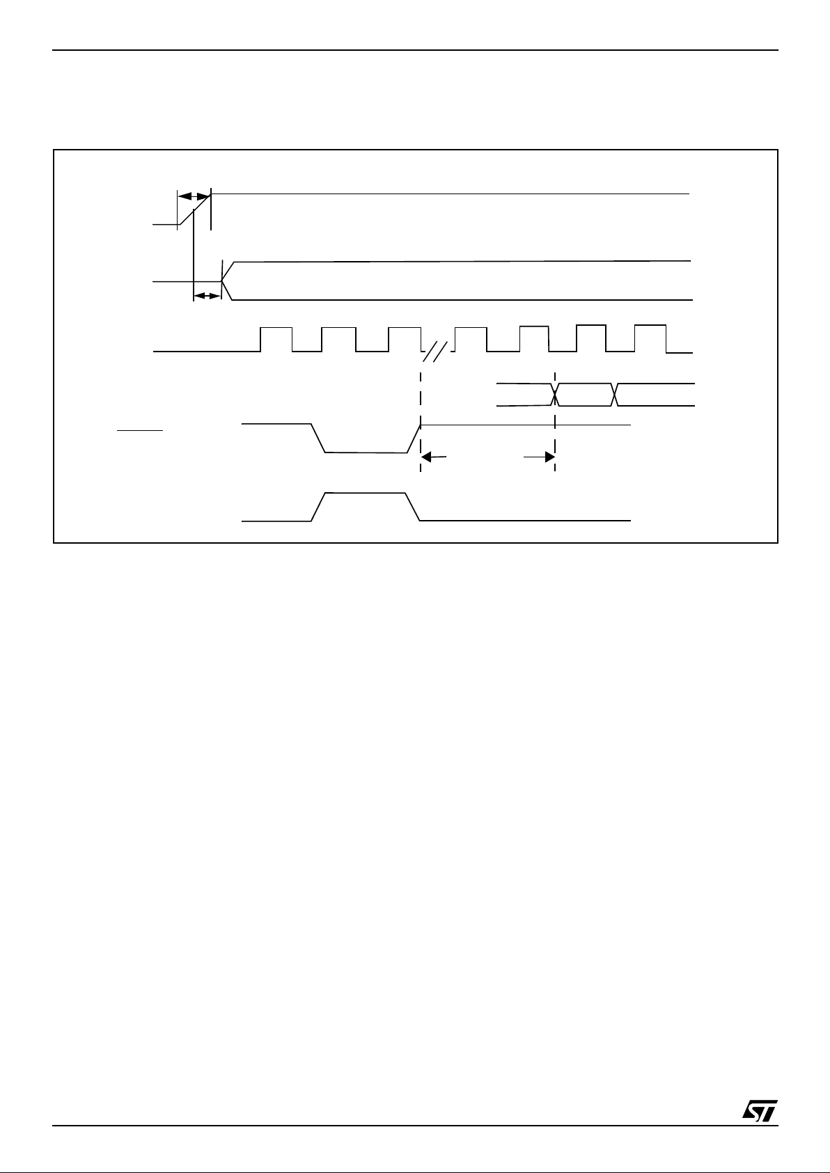
ST7263B
18/132
RESET (Cont’d)
Figure 12. Reset Timing Diagra m
Note: Refer to Electrical Characteristics for values of t
DDR
, t
OXOV
, V
IT+
, V
IT-
and V
hys
V
DD
OSCIN
f
CPU
FFFF
FFFE
PC
RESET
WATCHDOG RESET
t
DDR
t
OXOV
4096 CPU
CLOCK
CYCLES
DELAY
ST7263B
19/132
6.2 CLOCK SYSTEM
6.2.1 General Description
The MCU accepts either a Crystal or Ceramic res-
onator, or an external clock signal to drive the in-
ternal oscillator. The internal clock (f
CPU
) is de-
rived from the external oscillator frequency (f
OSC
),
which is divided by 3 (and by 2 or 4 for USB, de-
pending on the externa l clock used). The in ternal
clock is further divided by 2 by setting the SMS bit
in the Miscellaneous Register.
Using the OSC24/12 bit in the option byte, a 12
MHz or a 24 MHz external clo ck can be used to
provide an internal frequency of either 2, 4 or 8
MHz while mainta ining a 6 MHz for the US B (ref e r
to Figure 15 ).
The internal clock signal (f
CPU
) is also routed to
the on-chip peripherals. The CPU clock signal
consists of a square wave with a duty cycle of
50%.
The internal oscillat or is designed to operate with
an AT-cut parallel resonant quartz or ceramic res-
onator in the frequency range specified for f
osc
.
The circuit shown in Figure 14 is recommended
when using a crystal, and Tab le 6, "Recom mend-
ed Values for 24 MHz Crystal Resonator" lists th e
recommended capacitance. The crystal and asso-
ciated components should be mounted as close as
possible to the input pins in order to minimize out-
put distortion and start-up stabilisation time.
Table 6. Recommended Values for 24 MHz
Crystal Resonator
Note: R
SMAX
is the equivalent serial resistor of the
crystal (see crystal specification).
6.2.2 External Clock
An external clock may be applied to the OSCIN in-
put with the OSCOUT pin not connected, as
shown on F igure 13. The t
OXOV
specifications do
not apply when using an external clock input. The
equivalent specification of the external clock
source should be used instead of t
OXOV
(see Sec-
tion 6.5 CONTROL TIMING).
Figure 13. External Clock Source Connections
Figure 14. Crystal/Ceramic Resonator
Figure 15. Clock Block Diagram
R
SMAX
20
Ω
25
Ω
70
Ω
C
OSCIN
56pF 47pF 22pF
C
OSCOUT
56pF 47pF 22pF
R
P
1-10 M
Ω
1-10 M
Ω
1-10 M
Ω
OSCIN
OSCOUT
EXTERNAL
CLOCK
NC
OSCIN OSCOUT
C
OSCIN
C
OSCOUT
R
P
%3
CPU and
8, 4 or 2 MHz
6 MHz (USB)
24 or
peripherals)
%2
1
0
%2
12 MHz
Crystal
%2
0
1
OSC24/12
SMS
%2

ST7263B
20/132
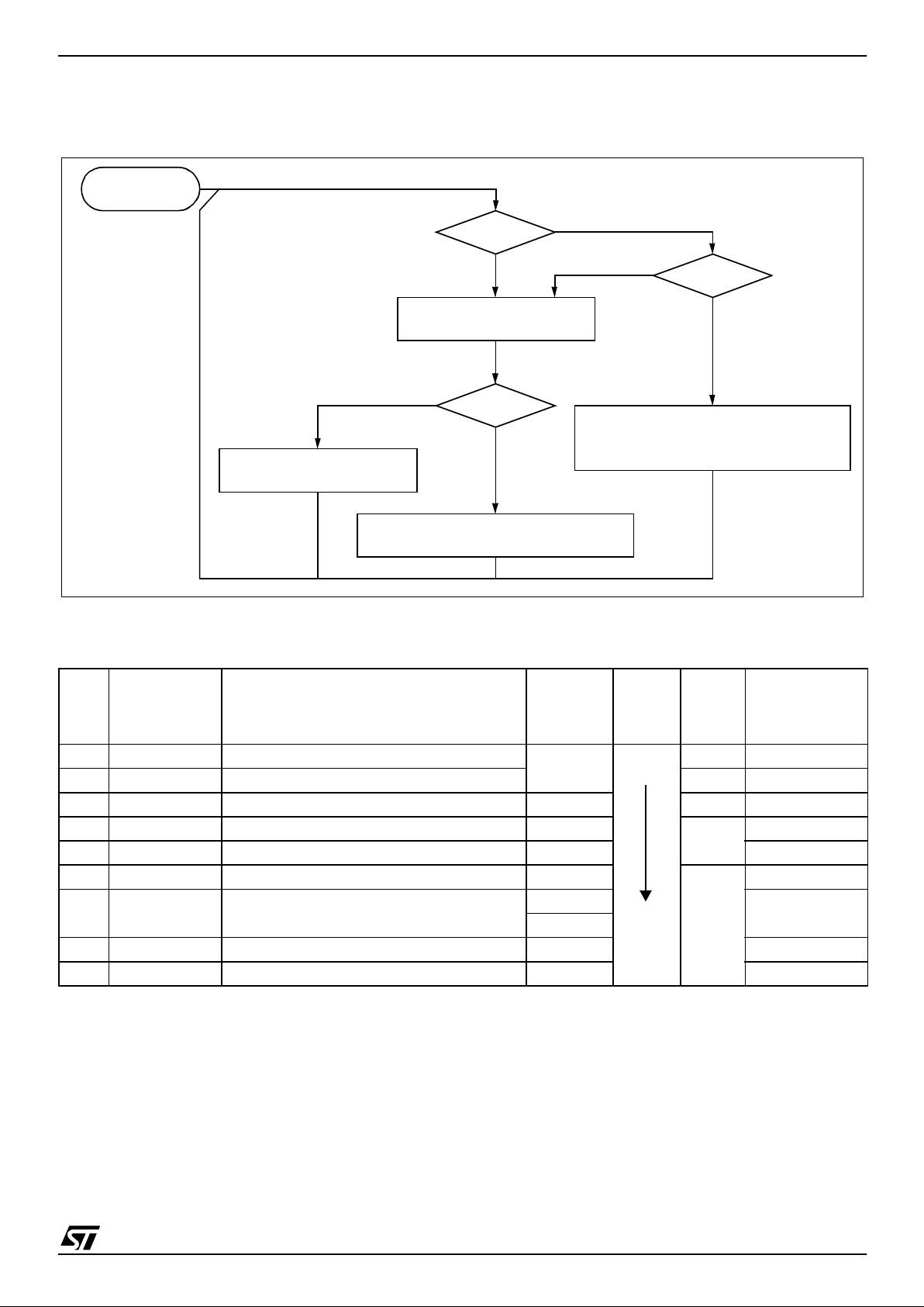
7 INTERRUPTS
The ST7 core may be interrupted by one of two dif-
ferent methods: maskable hardware interrupts as
listed in Table 7, "Interrupt Mapping" and a non-
maskable software interrupt (TRAP). The Interrupt
processing flowchart is shown in Figure 16.
The maskable interrupts must be enabled clearing
the I bit in order to be serviced. However, disabled
interrupts may be latched and processed when
they are enabled (see external interrupts subs ec-
tion ).
When an interrupt has to be serviced:
– Normal processing is susp ended at the end of
the current instruction execution.
– The PC, X, A and CC registers are saved onto
the stack.
– The I bit of the CC register is set to prevent addi-
tional interrupts.
– The PC is then loaded with the interrupt vector of
the interrupt to service and the first instruction of
the interrupt service routine is fetched (refer to
Table 7, "Interrupt Mapping" for vector address-
es).
The interrupt service routine should finish with the
IRET instruction w hich causes the contents of the
saved registers to be recovered from the stack.
Note: As a consequence of the IRET instruction,
the I bit will be cl eared and the main p rogram will
resume.
Priority Management
By default, a servicing interrupt cannot be inter-
rupted because the I bi t is set by hardware ent er-
ing in interrupt routine.
In the case several interrupts are simultaneously
pending, a hardware priority defines which one will
be serviced first (see Table 7, "Interrupt Map-
ping").
Non-maskable Software Interrupts
This interrupt is entered when the TRAP instruc-
tion is executed regardless of the state of the I bit.
It will be serviced according to the flowchart on
Figure 16.
Interrupts and Low Power Mode
All interrupts allow the processor to leave the Wait
low power mode. Only external and spe cific men-
tioned interrupts allow the processor to leave the
Halt low power mode (refer to t he “Exit from HALT“
column in Table 7, "Interrupt Mapping").
External Inte rru pt s
The pins ITi/PAk and ITj/ PBk (i= 1,2; j= 5,6 ; k=4,5)
can generate a n interrupt when a rising edge oc-
curs on this pin. Conversely, the ITl/PAn and ITm/
PBn pins (l=3,4; m= 7,8; n=6,7) can generate an
interrupt when a falling edge occurs on this pin.
Interrupt generation will occur if it is enabl ed with
the ITiE bit (i=1 to 8) in the ITRFRE register and if
the I bit of the CCR is reset.
Peripheral Interrupts
Different peripheral interrupt flags in the status
register are able to cause an interrupt when they
are active if both:
– The I bit of the CC register is cleared.
– The corresponding enable bit is set in the control
register.
If any of these two conditions is false, the interrupt
is latched and thus remains pending.
Clearing an interrupt request is done by one of the
two following operations:
– Writing “0” to the corresponding bit in the status
register.
– Accessing the status register while the flag is set
followed by a read or write of an associated reg-
ister.
Notes:
1. The clearing sequence resets the internal latch.
A pending interrupt (i.e. waiting to be enabled) will
therefore be lost if the clear sequence is executed.
2. All interrupts allow the processor to leave the
Wait low power mode.
3. Exit from Halt mode may only be triggered by an
External Interrupt on one of the ITi ports (PA4-PA7
and PB4-PB7), an end suspend mode Interrupt
coming from USB peripheral, or a reset.
ST7263B
21/132
INTERRUPTS (Cont’d)
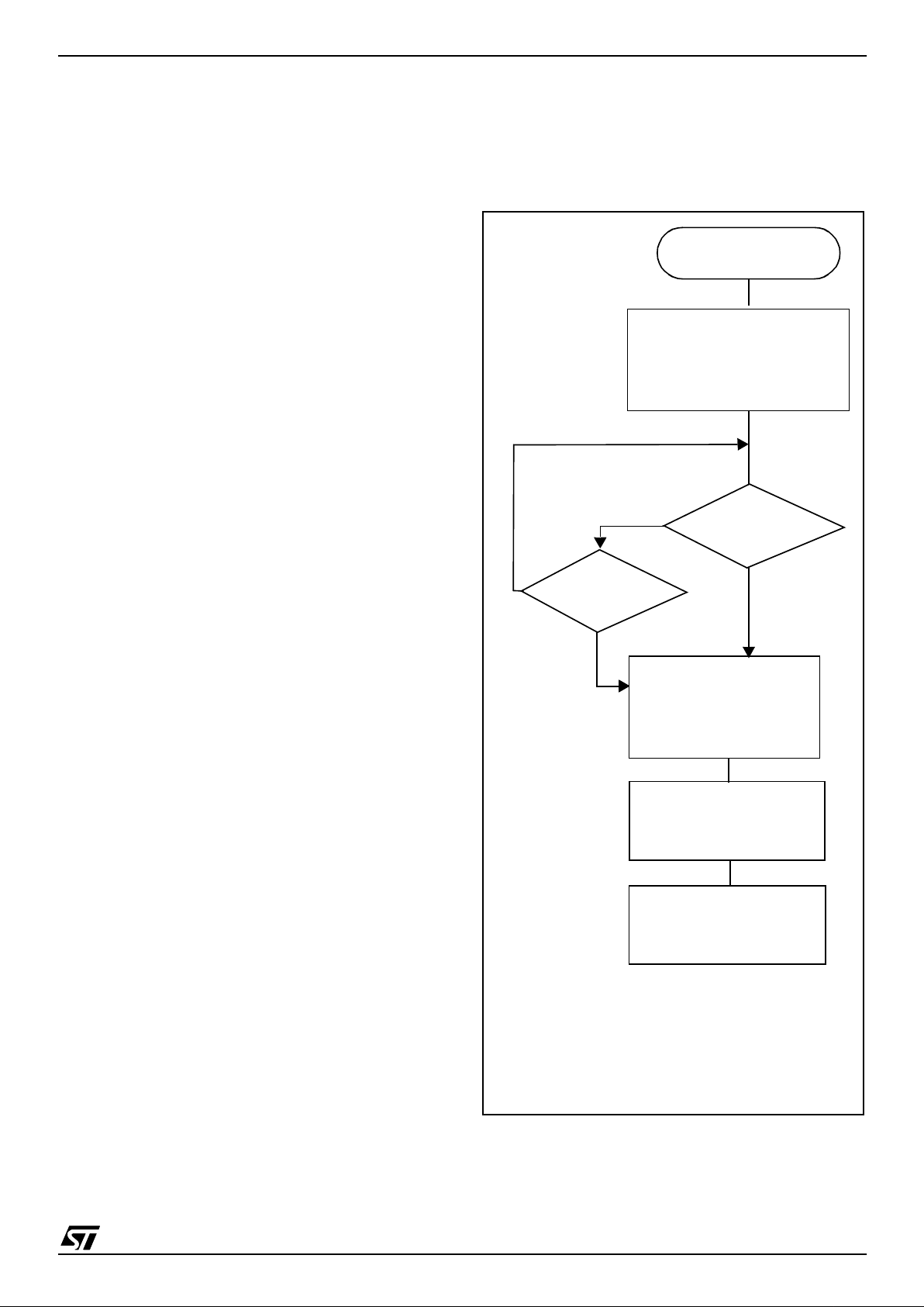
Figure 16. I nte rru pt P roce ssing Flow c hart
Table 7. I nte rrupt Mapping
BIT I SET
Y
N
IRET
Y
N
FROM RESET
LOAD PC FROM INTERRUPT VECTOR
STACK PC, X, A, CC
SET I BIT
FETCH NEXT INSTRUCTION
EXECUTE INSTRUCTION
THIS CLEARS I BIT BY DEFAULT
RESTORE PC, X, A, CC FROM STACK
INTERRUPT
Y
N
N°
Source
Block
Description
Register
Label
Priority
Order
Exit
from
HALT
Vector
Address
RESET Reset
N/A
Highest
Priority
Lowest
Priority
yes FFFEh-FFFFh
TRAP Software Interrupt no FFFCh-FFFDh
FLASH Flash Start Programming Interrupt yes FFFAh-FFFBh
USB End Suspend Mode ISTR
yes
FFF8h-FFF9h
1 ITi External Interrupts ITRFRE FFF6h-FFF7h
2 TIMER Timer Peripheral Interrupts TIMSR
no
FFF4h-FFF5h
3 I²C I²C Peripheral Interrupts
I²CSR1
FFF2h-FFF3h
I²CSR2
4 SCI SCI Peripheral Interr upts SCISR FFF0h-FFF1h
5 USB USB Peripheral Interrupts ISTR FFEEh-FFEFh

ST7263B
22/132
INTERRUPTS (Cont’d)
7.1 Interrupt Register
INTERRUPTS REGISTER (ITRFRE)
Address: 0008h — Read/Write
Reset Value: 0000 0000 (00h)
Bit 7:0 = ITiE (i=1 to 8).
Interrupt Enable Control
Bits
.
If an ITiE bit is set, the corresponding interrupt is
generated when
– a rising edge occurs on the pin PA4/IT1 or PA5/
IT2 or PB4/IT5 or PB5/IT6
or
– a falling edge occurs on the pin PA6/IT3 or PA7/
IT4 or PB6/IT7 or PB7/IT8
No interrupt is generated elsewhere.
Note: Analog input must be disabled for interrupts
coming from port B.
70
IT8E IT7E IT6E IT5E IT4E IT3E IT 2E IT1E
ST7263B
23/132
8 POWER SAVING MODES
8.1 Introduction
To give a large measure of flexibility to the applica-
tion in terms of power consumption, two main pow-
er saving modes are implemented in the ST7.
After a RESET, the normal operating mode is se-
lected by default (RUN mode). This mode drives
the device (CPU and embedded peripherals) by
means of a master clock which is based on the
main oscillator frequency divided by 3 (f
CPU
).
From Run mode, the different power saving
modes may be selected by setting the relevant
register bits or by calling the specific ST7 software
instruction whose action depends on the oscillator
status.
8.2 HALT Mode
The MCU consumes the least amount of power i n
HALT mode. The HALT mode is entered by exe-
cuting the HALT instruction. The internal oscillator
is then turned off, causing all internal processing to
be stopped, including the operation of the on-chip
peripherals.
When entering HALT mode, the I bit in the Condi-
tion Code Register is cleared. Thus, all external in-
terrupts (ITi or USB end suspend mode) are al-
lowed and if an interrupt occurs, the CPU clock be-
come s a ctive.
The MCU can e xit HAL T mode on reception of ei-
ther an external interrupt on ITi, an end suspen d
mode interrupt coming from USB peripheral, or a
reset. The osc illato r is t hen t ur ned on and a stabi-
lization time is provided before rele as ing CPU op-
eration. The stabilization time is 4096 CPU clock
cycles.
After the start up delay, the CPU continues opera-
tion by servicing the interrupt which wakes it up or
by fetching the reset vector if a reset wakes it up.
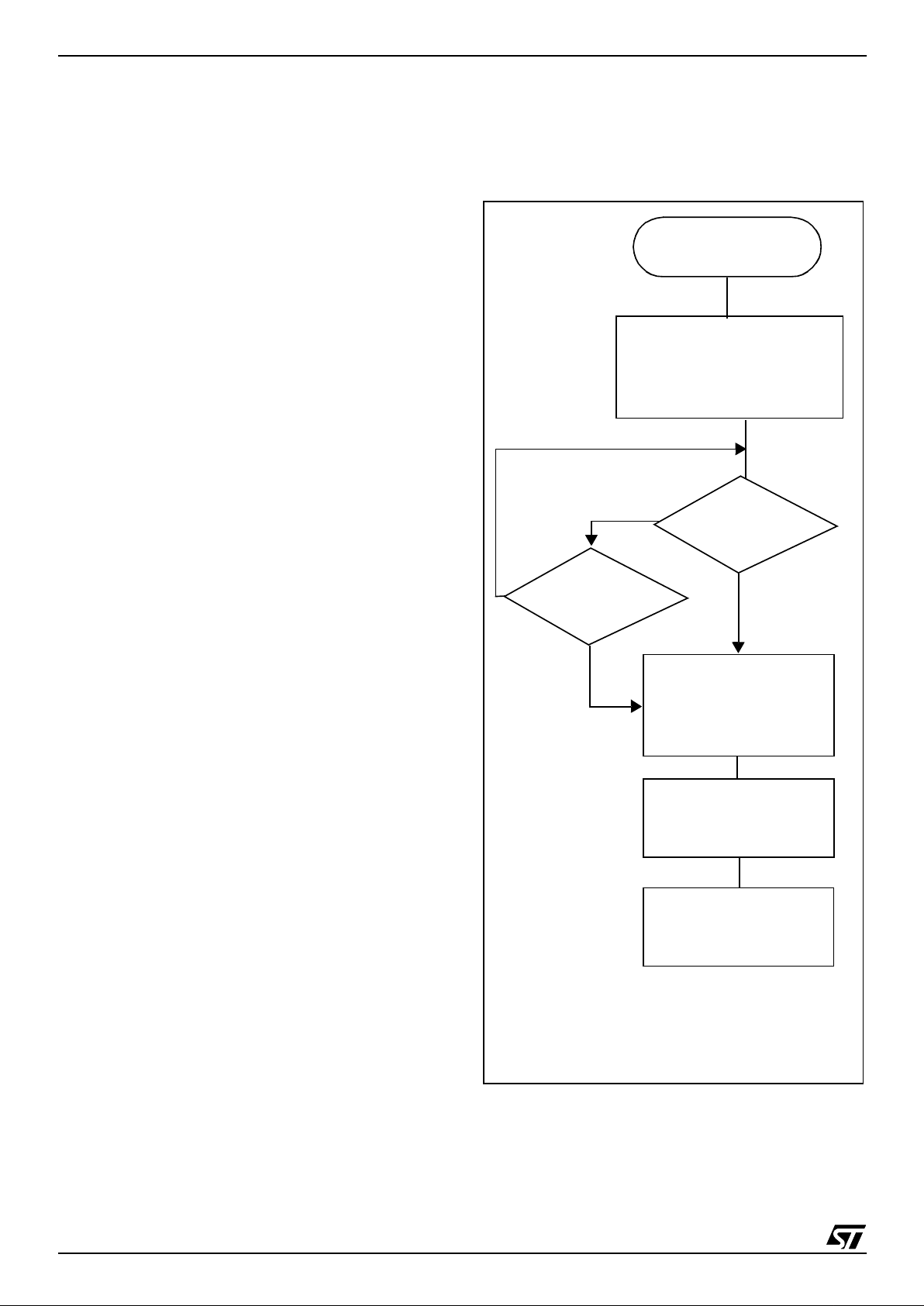
Figure 17. HALT Mod e Flo w C hart
N
N
EXTERNAL
INTERRUPT*
RESET
HALT INSTRUCTION
4096 CPU CLOCK
FETCH RESET VECTOR
OR SERVICE INTERRUPT
CYCLES DELAY
CPU CLOCK
OSCILLATOR
PERIPH. CLOCK
I-BIT
ON
ON
SET
ON
CPU CLOCK
OSCILLATOR
PERIPH. CLOCK
I-BIT
OFF
OFF
CLEARED
OFF
Y
Y
Note: Before servicing an interrupt, the CC register is
pushed on the stac k. T he I -Bit i s se t du ring the inter-
rupt routine and cleared when the CC register is
popped.
ST7263B
24/132
POWER SAVING MODES (Cont’d)
8.3 SLOW Mode
In Slow mode, the osc illator frequency can be d i-
vided by 2 as selected by the SMS bit in the Mis-
cellaneous Register. The CPU and peripherals are
clocked at this lower frequency. Slow mode is
used to reduce power co nsumption, and enables
the user to adapt the clock frequency to the avail-
able supply voltage.
8.4 WAIT Mode
WAIT mode places the MCU in a low power c on-
sumption mode by stopping the CPU.
This pow e r s a v ing mo de is selected by calling the
“WFI” ST7 software instruction.
All peripherals remain active. During WAIT mode,
the I bit of t he CC register is f orced t o 0 to enabl e
all interrupts. All other registers and memory re-
main unchanged. The MCU remains in WAIT
mode until an interrupt or Res et oc curs, where up-
on the Program Counter branches to the starting
address of the interrupt or Reset service routine.
The MCU w ill re mai n in W AIT mo de unt il a Res et
or an Interrupt occurs, causing it to wake up.
Refer to Figure 18.
Figure 18. WAIT Mode Flow Chart
WFI INSTRUCTION
RESET
INTERRUPT
Y
N
N
Y
CPU CLOCK
OSCILLATOR
PERIPH. CLOCK
I-BIT
ON
ON
CLEARED
OFF
CPU CLOCK
OSCILLATOR
PERIPH. CLOCK
I-BIT
ON
ON
SET
ON
FETCH RESET VECTOR
OR SERVICE INTERRUPT
4096 CPU CLOCK
CYCLES DELAY
IF RESET
Note: Before servicing an interrupt, the CC register is
pushed on the sta ck. The I-Bit is s et d uring the inte r-
rupt routine and cleared when the CC register is
popped.
ST7263B
25/132
9 I/O PORTS
9.1 Introduction
The I/O ports offer different functional modes:
– Transfer of data through digital inputs and out-
puts and for specific pins
– Analog signal input (ADC)
– Alternate signal input/out put for the on-chip pe-
ripherals
– External interrupt generation
An I/O port consists o f up to 8 p ins. Each pin can
be programmed independently as a digital input
(with or without interrupt generation) or a digital
output.
9.2 Functional description
Each port is associated to 2 main registers:
– Data Register (DR)
– Data Direction Register (DDR)
Each I/O pin may be programmed using the corre-
sponding register bits in DDR register: bit X corre-
sponding to pin X of the port. The same corre-
spondence is used for the DR register.
Table 8. I /O Pi n Fu nc ti ons
Input Modes
The input configuration is s ele cted by clearing the
corresponding DDR register bit.
In this case, reading the DR register returns the
digital value applied to the external I/O pin.
Note 1: All the inputs are triggered by a Schmitt
trigg er.
Note 2: When switching from input mode to output
mode, the DR register should be written first to
output the correct value as soon as the port is con-
figured as an output.
Interrupt function
When an I/O is configured as an Input with Inter-
rupt, an event on this I/O can generate an external
Interrupt request to the CPU. The interrupt sensi-
tivity is given indepe ndently according to the de-
scription mentioned in the ITRFRE in terrupt regis-
ter.
Each pin can independently generate an I nterrupt
request.
Each external interrupt vecto r is linked to a dedi-
cated group of I/O port pins (see Interrupts sec-
tion). If more than one input pin is selected sim ul-
taneously as an interrupt source, this is logically
ORed. For this reason if one of the interrupt pins is
tied low, the other ones are masked.
Output Mode
The pin is configured in output mode by setting the
corresponding DDR register bit (see Table 7).
In this mode, writing “0” or “1” to the DR register
applies this digital value to the I/O pin through the
latch. Therefore, t he previously s aved value is re-
stored when the DR register is read.
Note: The interrupt function is disabled in this
mode.
Digital A lternate Func ti on
When an on-chip peripheral is configured to use a
pin, the alternate function is au tomatically select-
ed. This alternate function takes priority over
standard I/O programming. When the signal is
coming from an on-chip peripheral, the I/O pin is
automatically configured in output mode (push-pull
or open drain according to the peripheral).
When the signal is goi ng t o an on-c hip pe ripheral,
the I/O pin ha s to be configured in input m ode. In
this case, the pin’s state is also digitally reada ble
by addressing the DR register.
Notes:
1. Input pull-up conf iguration can cause a n unex-
pected value at the input of the alternate peripher-
al input.
2. When the on-chip peripheral uses a pin as input
and output, this pin must be configured as an input
(DDR = 0).
Warning
: The alternate f uncti on m ust not be acti-
vated as long as the p in is con figured as an input
with interrupt in order to avoid generating spurious
interrupts.
DDR MODE
0 Input
1 Output

ST7263B
26/132
I/O PORTS (Cont’d)
Analog Alternate Function
When the pin is used as an ADC input the I/O must
be configured as a floating input. The analog mu l-
tiplexer (controlled by the ADC registers) switches
the analog voltage pre sent on the selected pin t o
the common ana log ra il which i s connec ted to the
ADC input.
It is recommended not to change the voltage level
or loading on any port pin while conversion is in
progress. Furthermore it is recommended not to
have clocking pins located c lose to a selected an-
alog pin.
Warning
: The analog input voltage level must be
within the limits s tated in the A bsolute Ma ximum
Ratings.
9.3 I/O Port Implementation
The hardware implementation on each I/O port de-
pends on the settings in the DDR register and spe-
cific feature of the I/O port such as ADC Input or
true open drain.
ST7263B
27/132
I/O PORTS (Cont’d)
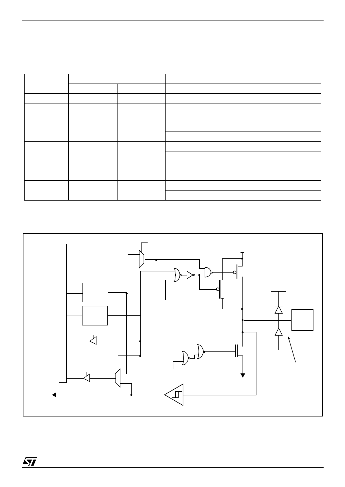
9.3.1 Port A
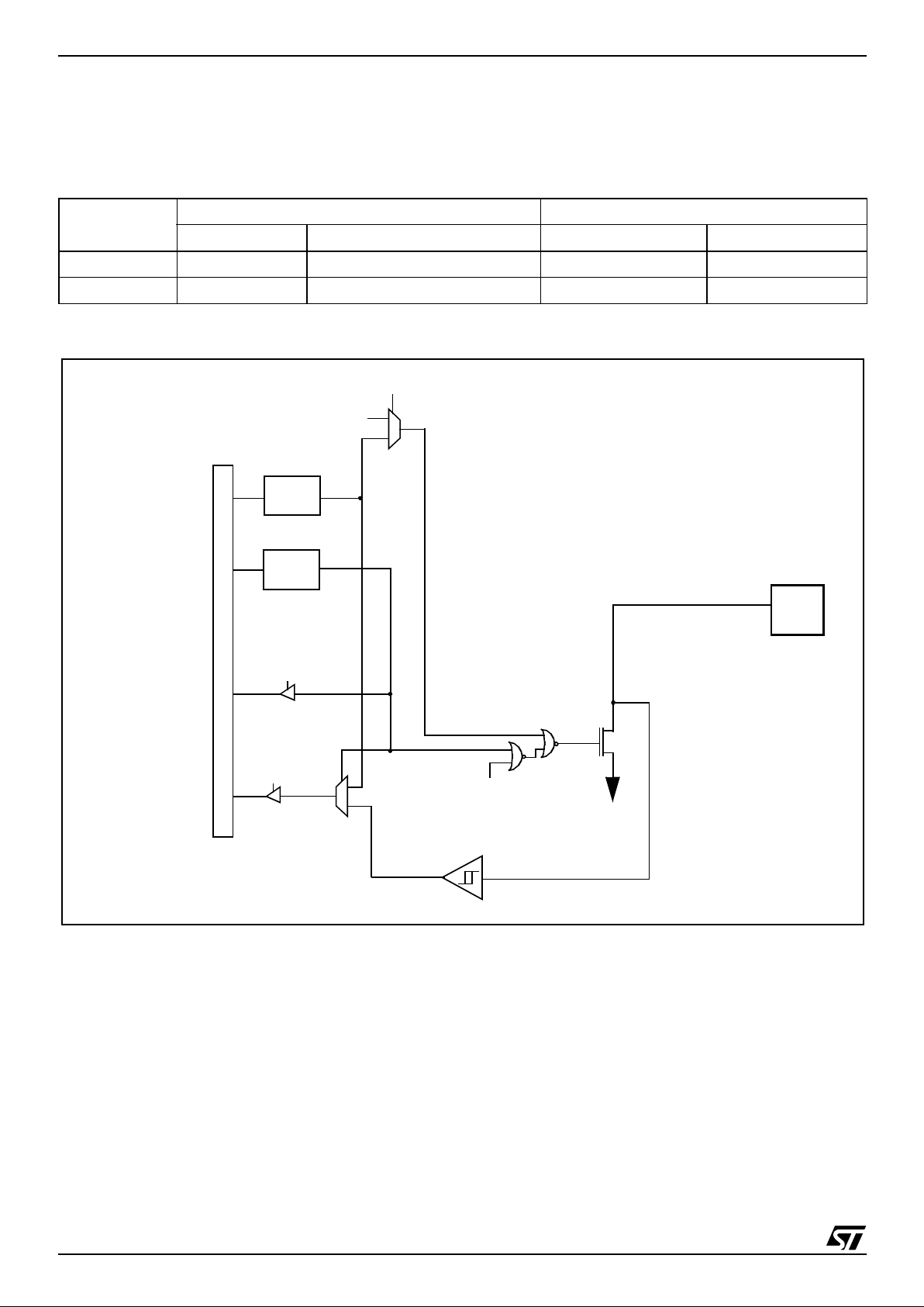
Table 9. Port A0, A3, A4, A5, A6, A7 Description
Figure 19. PA0, PA3, PA4, PA5, PA6, PA7 Configuration
PORT A
I / O Alternate Function
Input* Output Signal Condition
PA0 with pull-up push-pull MCO (Main Clock Output) MCO = 1 (MISCR)
PA3 with pull-up push-pull Timer EXTCLK
CC1 =1
CC0 = 1 (Timer CR2)
PA4 with pull-up
push-pull
Timer ICAP1
IT1 Schmitt triggered input IT1E = 1 (ITIFRE)
PA5 with pull-up
push-pull
Timer ICAP2
IT2 Schmitt triggered input IT2E = 1 (ITIFRE)
PA6 with pull-up
push-pull
Timer OCMP1 OC1E = 1
IT3 Schmitt triggered input IT3E = 1 (ITIFRE)
PA7 with pull-up
push-pull
Timer OCMP2 OC2E = 1
IT4 Schmitt triggered input IT4E = 1 (ITIFRE)
*Reset State
DR
DDR
LATCH
LATCH
DR SEL
DDR SEL
V
DD
PAD
ALTERNATE ENABLE
ALTERNATE ENABLE
ALTERNATE ENABLE
ALTERNATE
ALTERNATE INPUT
PULL-UP
OUTPUT
P-BUFFER
N-BUFFER
1
0
1
0
CMOS SCHMITT TRIGGER
V
SS
V
DD
DIODES
DATA BUS
ST7263B
28/132
I/O PORTS (Cont’d)
Table 10. PA1, PA2 Description
Figure 20. PA1, PA2 Configuration
PORT A
I / O Alternate Function
Input* Output Signal Condition
PA1 without pull-up Very High Current open drain SDA (I²C data) I²C enable
PA2 without pull-up Very High Current open drain SCL (I²C clock) I²C enable
*Reset State
DR
DDR
LATCH
LATCH
DR SEL
DDR SEL
PAD
ALTERNATE ENABLE
ALTERNATE ENABLE
ALTERNATE
OUTPUT
N-BUFFER
1
0
1
0
CMOS SCHMITT TRIGGER
V
SS
DATA BUS
ST7263B
29/132
I/O PORTS (Cont’d)
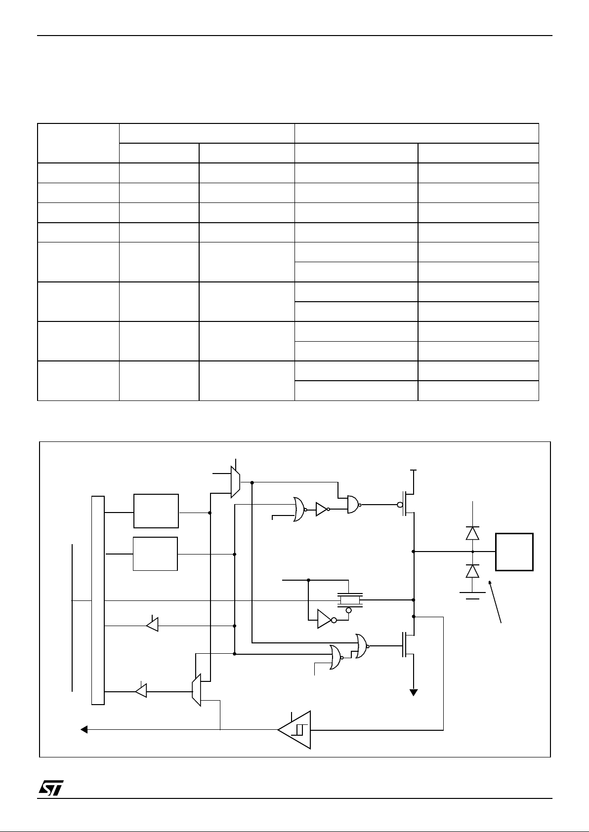
9.3.2 Port B
Table 11. Port B Description
Figure 21. Port B Conf i gu ra ti on
PORT B I/O Alternate Function
Input* Output Signal Condition
PB0 without pull-up push-pull Analog input (ADC) CH[2:0] = 000 (ADCCSR)
PB1 without pull-up push-pull Analog input (ADC) CH[2:0] = 001 (ADCCSR)
PB2 without pull-up push-pull Analog input (ADC) CH[2:0]= 010 (ADCCSR)
PB3 without pull-up push-pull Analog input (ADC) CH[2:0]= 011 (ADCCSR)
PB4 without pull-up push-pull
Analog input (ADC) CH[2:0]= 100 (ADCCS R)
IT5 Schmitt triggered input IT4E = 1 (ITIFRE)
PB5 without pull-up push-pull
Analog input (ADC) CH[2:0]= 101 (ADCCS R)
IT6 Schmitt triggered input IT5E = 1 (ITIFRE)
PB6 without pull-up push-pull
Analog input (ADC) CH[2:0]= 110 (ADCCS R)
IT7 Schmitt triggered input IT6E = 1 (ITIFRE)
PB7 without pull-up push-pull
Analog input (ADC) CH[2:0]= 111 (ADCCS R)
IT8 Schmitt triggered input IT7E = 1 (ITIFRE)
*Reset State
DR
DDR
LATCH
LATCH
DR SEL
DDR SEL
V
DD
PAD
ANALOG
SWITCH
ANALOG ENABLE
(ADC)
ALTERNATE ENABLE
ALTERNATE ENABLE
DIGITA L EN AB L E
ALTE RN AT E ENABLE
ALTER NAT E
ALTERN AT E INPUT
OUTPUT
P-BUFFER
N-BU FF E R
1
0
1
0
V
SS
DATA BUS
COMMON ANALOG RAIL
V
DD
DIODES
ST7263B
30/132
I/O PORTS (Cont’d)
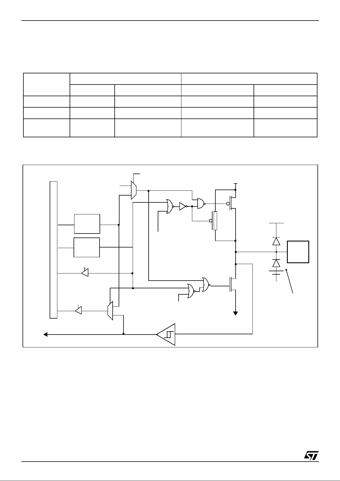
9.3.3 Port C
Table 12. Port C Description
Figure 22. P ort C C onfi guration
PORT C
I / O Alternate Function
Input* Output Signal Condition
PC0 with pull-up push-pull RDI (SCI input)
PC1 with pull-up push-pull TDO (SCI output) SCI enable
PC2 with pull-up push-pull
USBOE (USB output ena-
ble)
USBOE =1
(MISCR)
*Reset State
DR
DDR
LATCH
LATCH
DR SEL
DDR SEL
V
DD
PAD
ALTE RN AT E ENABLE
ALTERNATE ENABLE
ALTERNATE ENABLE
ALTERNATE
ALTERNATE INPUT
PULL-UP
OUTPUT
P-BUFFER
N-BUFFER
1
0
1
0
CMOS SCHMITT TRIGGER
V
SS
V
DD
DATA BUS
DIODES
 Loading...