


SGS Thomson Microelectronics ST62T62BM6, ST62T62BM3, ST62T52BM6, ST62T52BM3, ST62P52BM6 Datasheet
... R
R
ST62T52B
ST62T62B/E62B
8-BIT OTP/EPROM MCUs WITH
A/D CONVERTER, AUTO-RELOAD TIMER AND EEPROM
■3.0 to 6.0V Supply Operating Range
■8 MHz Maximum Clock Frequency
■-40 to +125°C Operating Temperature Range
■Run, Wait and Stop Modes
■5 Interrupt Vectors
■Look-up Table capability in Program Memory
■Data Storage in Program Memory: User selectable size
■Data RAM: 128 bytes
■Data EEPROM: 64 bytes (none on ST62T52B)
■User Programmable Options
■9 I/O pins, fully programmable as:
–Input with pull-up resistor
–Input without pull-up resistor
–Input with interrupt generation
–Open-drain or push-pull output
–Analog Input
■5 I/O lines can sink up to 20mA to drive LEDs or TRIACs directly
■8-bit Timer/Counter with 7-bit programmable prescaler
■8-bit Auto-reload Timer with 7-bit programmable prescaler (AR Timer)
■Digital Watchdog
■8-bit A/D Converter with 4 analog inputs
■On-chip Clock oscillator can be driven by Quartz Crystal Ceramic resonator or RC network
■User configurable Power-on Reset
■One external Non-Maskable Interrupt
■ST626x-EMU2 Emulation and Development System (connects to an MS-DOS PC via a parallel port)
DEVICE SUMMARY
DEVICE |
EPROM |
OTP |
EEPROM |
|
(Bytes) |
(Bytes) |
|||
|
|
|||
|
|
|
|
|
ST62T52B |
|
1836 |
- |
|
|
|
|
|
|
ST62T62B |
|
1836 |
64 |
|
|
|
|
|
|
ST62E62B |
1836 |
|
64 |
|
|
|
|
|
PDIP16
PSO16
CDIP16W
(See end of Datasheet for Ordering Information)
Rev. 2.4
April 1998 |
1/68 |

Table of Contents
ST62T52B / ST62T62B/E62B . . . . . . . . . . . . . . . . . . . . . . . . . . . 1
1 GENERAL DESCRIPTION . . . . . . . . . . . . . . . . . . . . . . . . . . . . . . . . . . . . . . . . . . . . . . . . . . . . . |
. 4 |
||
1.1 |
INTRODUCTION . . . . . . . . . . . . . . . . . . . . . . . . . . . . . . . . . . . . . . . . . . . . . . . . . . . . . . . . . |
4 |
|
1.2 |
PIN DESCRIPTIONS . . . . . . . . . . . . . . . . . . . . . . . . . . . . . . . . . . . . . . . . . . . . . . . . . . . . . . |
5 |
|
1.3 |
MEMORY MAP . . . . . . . . . . . . . . . . . . . . . . . . . . . . . . . . . . . . . . . . . . . . . . . . . . . . . . . . . . |
6 |
|
|
1.3.1 |
Introduction . . . . . . . . . . . . . . . . . . . . . . . . . . . . . . . . . . . . . . . . . . . . . . . . . . . . . . . . |
6 |
|
1.3.2 |
Program Space . . . . . . . . . . . . . . . . . . . . . . . . . . . . . . . . . . . . . . . . . . . . . . . . . . . . . |
7 |
|
1.3.3 |
Data Space . . . . . . . . . . . . . . . . . . . . . . . . . . . . . . . . . . . . . . . . . . . . . . . . . . . . . . . . |
8 |
|
1.3.4 |
Stack Space . . . . . . . . . . . . . . . . . . . . . . . . . . . . . . . . . . . . . . . . . . . . . . . . . . . . . . . . |
8 |
|
1.3.5 |
Data Window Register (DWR) . . . . . . . . . . . . . . . . . . . . . . . . . . . . . . . . . . . . . . . . . . |
9 |
|
1.3.6 Data RAM/EEPROM Bank Register (DRBR) . . . . . . . . . . . . . . . . . . . . . . . . . . . . . . |
10 |
|
|
1.3.7 |
EEPROM Description . . . . . . . . . . . . . . . . . . . . . . . . . . . . . . . . . . . . . . . . . . . . . . . |
11 |
1.4 |
PROGRAMMING MODES . . . . . . . . . . . . . . . . . . . . . . . . . . . . . . . . . . . . . . . . . . . . . . . . . |
13 |
|
1.4.1 Option Byte . . . . . . . . . . . . . . . . . . . . . . . . . . . . . . . . . . . . . . . . . . . . . . . . . . . . . . . 13
1.4.2 Program Memory . . . . . . . . . . . . . . . . . . . . . . . . . . . . . . . . . . . . . . . . . . . . . . . . . . . 13
1.4.3 . EEPROM Data Memory . . . . . . . . . . . . . . . . . . . . . . . . . . . . . . . . . . . . . . . . . . . . . 13
2 CENTRAL PROCESSING UNIT . . . . . . . . . . . . . . . . . . . . . . . . . . . . . . . . . . . . . . . . . . . . . . . . . |
14 |
||
2.1 |
INTRODUCTION . . . . . . . . . . . . . . . . . . . . . . . . . . . . . . . . . . . . . . . . . . . . . . . . . . . . . . . . |
14 |
|
2.2 |
CPU REGISTERS . . . . . . . . . . . . . . . . . . . . . . . . . . . . . . . . . . . . . . . . . . . . . . . . . . . . . . . |
14 |
|
3 CLOCKS, RESET, INTERRUPTS AND POWER SAVING MODES . . . . . . . . . . . . . . . . . . . . . |
16 |
||
3.1 |
CLOCK SYSTEM . . . . . . . . . . . . . . . . . . . . . . . . . . . . . . . . . . . . . . . . . . . . . . . . . . . . . . . . |
16 |
|
|
3.1.1 |
Main Oscillator . . . . . . . . . . . . . . . . . . . . . . . . . . . . . . . . . . . . . . . . . . . . . . . . . . . . . |
16 |
3.2 |
RESETS . . . . . . . . . . . . . . . . . . . . . . . . . . . . . . . . . . . . . . . . . . . . . . . . . . . . . . . . . . . . . . . |
18 |
|
|
3.2.1 |
RESET Input . . . . . . . . . . . . . . . . . . . . . . . . . . . . . . . . . . . . . . . . . . . . . . . . . . . . . . |
18 |
|
3.2.2 |
Power-on Reset . . . . . . . . . . . . . . . . . . . . . . . . . . . . . . . . . . . . . . . . . . . . . . . . . . . . |
18 |
|
3.2.3 |
Watchdog Reset . . . . . . . . . . . . . . . . . . . . . . . . . . . . . . . . . . . . . . . . . . . . . . . . . . . |
19 |
|
3.2.4 |
Application Notes . . . . . . . . . . . . . . . . . . . . . . . . . . . . . . . . . . . . . . . . . . . . . . . . . . . |
19 |
|
3.2.5 |
MCU Initialization Sequence . . . . . . . . . . . . . . . . . . . . . . . . . . . . . . . . . . . . . . . . . . |
19 |
3.3 |
DIGITAL WATCHDOG . . . . . . . . . . . . . . . . . . . . . . . . . . . . . . . . . . . . . . . . . . . . . . . . . . . . |
21 |
|
|
3.3.1 |
Digital Watchdog Register (DWDR) . . . . . . . . . . . . . . . . . . . . . . . . . . . . . . . . . . . . . |
23 |
|
3.3.2 |
Application Notes . . . . . . . . . . . . . . . . . . . . . . . . . . . . . . . . . . . . . . . . . . . . . . . . . . . |
23 |
3.4 |
INTERRUPTS . . . . . . . . . . . . . . . . . . . . . . . . . . . . . . . . . . . . . . . . . . . . . . . . . . . . . . . . . . |
25 |
|
|
3.4.1 |
Interrupt request . . . . . . . . . . . . . . . . . . . . . . . . . . . . . . . . . . . . . . . . . . . . . . . . . . . . |
25 |
|
3.4.2 |
Interrupt Procedure . . . . . . . . . . . . . . . . . . . . . . . . . . . . . . . . . . . . . . . . . . . . . . . . . |
26 |
|
3.4.3 |
Interrupt Option Register (IOR) . . . . . . . . . . . . . . . . . . . . . . . . . . . . . . . . . . . . . . . . |
27 |
|
3.4.4 |
Interrupt Sources . . . . . . . . . . . . . . . . . . . . . . . . . . . . . . . . . . . . . . . . . . . . . . . . . . . |
27 |
3.5 |
POWER SAVING MODES . . . . . . . . . . . . . . . . . . . . . . . . . . . . . . . . . . . . . . . . . . . . . . . . . |
29 |
|
3.5.1 WAIT Mode . . . . . . . . . . . . . . . . . . . . . . . . . . . . . . . . . . . . . . . . . . . . . . . . . . . . . . . 29 3.5.2 STOP Mode . . . . . . . . . . . . . . . . . . . . . . . . . . . . . . . . . . . . . . . . . . . . . . . . . . . . . . . 29 3.5.3 Exit from WAIT and STOP Modes . . . . . . . . . . . . . . . . . . . . . . . . . . . . . . . . . . . . . . 30
4 ON-CHIP PERIPHERALS . . . . . . . . . . . . . . . . . . . . . . . . . . . . . . . . . . . . . . . . . . . . . . . . . . . . . . |
31 |
4.1 I/O PORTS . . . . . . . . . . . . . . . . . . . . . . . . . . . . . . . . . . . . . . . . . . . . . . . . . . . . . . . . . . . . . 31
4.1.1 Operating Modes . . . . . . . . . . . . . . . . . . . . . . . . . . . . . . . . . . . . . . . . . . . . . . . . . . . 32 4.1.2 Safe I/O State Switching Sequence . . . . . . . . . . . . . . . . . . . . . . . . . . . . . . . . . . . . . 33 4.1.3 ARTimer alternate functions . . . . . . . . . . . . . . . . . . . . . . . . . . . . . . . . . . . . . . . . . . 35 4.2 TIMER . . . . . . . . . . . . . . . . . . . . . . . . . . . . . . . . . . . . . . . . . . . . . . . . . . . . . . . . . . . . . . . . 36
2/68

Table of Contents
4.2.1 Timer Operation . . . . . . . . . . . . . . . . . . . . . . . . . . . . . . . . . . . . . . . . . . . . . . . . . . . . 37
4.2.2 Timer Interrupt . . . . . . . . . . . . . . . . . . . . . . . . . . . . . . . . . . . . . . . . . . . . . . . . . . . . . 37
4.2.3 Application Notes . . . . . . . . . . . . . . . . . . . . . . . . . . . . . . . . . . . . . . . . . . . . . . . . . . . 37
4.2.4 Timer Registers . . . . . . . . . . . . . . . . . . . . . . . . . . . . . . . . . . . . . . . . . . . . . . . . . . . . 38
4.3 AUTO-RELOAD TIMER . . . . . . . . . . . . . . . . . . . . . . . . . . . . . . . . . . . . . . . . . . . . . . . . . . . 39
4.3.1 AR Timer Description . . . . . . . . . . . . . . . . . . . . . . . . . . . . . . . . . . . . . . . . . . . . . . . . 39 4.3.2 Timer Operating Modes . . . . . . . . . . . . . . . . . . . . . . . . . . . . . . . . . . . . . . . . . . . . . . 39 4.3.3 AR Timer Registers . . . . . . . . . . . . . . . . . . . . . . . . . . . . . . . . . . . . . . . . . . . . . . . . . 43 4.4 A/D CONVERTER (ADC) . . . . . . . . . . . . . . . . . . . . . . . . . . . . . . . . . . . . . . . . . . . . . . . . . 45
4.4.1 Application Notes . . . . . . . . . . . . . . . . . . . . . . . . . . . . . . . . . . . . . . . . . . . . . . . . . . . 45
5 SOFTWARE . . . . . . . . . . . . . . . . . . . . . . . . . . . . . . . . . . . . . . . . . . . . . . . . . . . . . . . . . . . . . . . . |
47 |
5.1 ST6 ARCHITECTURE . . . . . . . . . . . . . . . . . . . . . . . . . . . . . . . . . . . . . . . . . . . . . . . . . . . . 47 5.2 ADDRESSING MODES . . . . . . . . . . . . . . . . . . . . . . . . . . . . . . . . . . . . . . . . . . . . . . . . . . . 47 5.3 INSTRUCTION SET . . . . . . . . . . . . . . . . . . . . . . . . . . . . . . . . . . . . . . . . . . . . . . . . . . . . . . 48
6 ELECTRICAL CHARACTERISTICS . . . . . . . . . . . . . . . . . . . . . . . . . . . . . . . . . . . . . . . . . . . . . . 53
6.1 ABSOLUTE MAXIMUM RATINGS . . . . . . . . . . . . . . . . . . . . . . . . . . . . . . . . . . . . . . . . . . . 53 6.2 RECOMMENDED OPERATING CONDITIONS . . . . . . . . . . . . . . . . . . . . . . . . . . . . . . . . . 54 6.3 DC ELECTRICAL CHARACTERISTICS . . . . . . . . . . . . . . . . . . . . . . . . . . . . . . . . . . . . . . 55 6.4 AC ELECTRICAL CHARACTERISTICS . . . . . . . . . . . . . . . . . . . . . . . . . . . . . . . . . . . . . . 56 6.5 A/D CONVERTER CHARACTERISTICS . . . . . . . . . . . . . . . . . . . . . . . . . . . . . . . . . . . . . . 56 6.6 TIMER CHARACTERISTICS . . . . . . . . . . . . . . . . . . . . . . . . . . . . . . . . . . . . . . . . . . . . . . . 57 6.7 SPI CHARACTERISTICS . . . . . . . . . . . . . . . . . . . . . . . . . . . . . . . . . . . . . . . . . . . . . . . . . 57 6.8 ARTIMER ELECTRICAL CHARACTERISTICS . . . . . . . . . . . . . . . . . . . . . . . . . . . . . . . . . 57
7 GENERAL INFORMATION . . . . . . . . . . . . . . . . . . . . . . . . . . . . . . . . . . . . . . . . . . . . . . . . . . . . . |
58 |
7.1 PACKAGE MECHANICAL DATA . . . . . . . . . . . . . . . . . . . . . . . . . . . . . . . . . . . . . . . . . . . . 58 7.2 ORDERING INFORMATION . . . . . . . . . . . . . . . . . . . . . . . . . . . . . . . . . . . . . . . . . . . . . . . 59
ST62P52B / ST62P62B . . . . . . . . . . . . . . . . . . . . . . . . . . . . . . . 61
1 GENERAL DESCRIPTION . . . . . . . . . . . . . . . . . . . . . . . . . . . . . . . . . . . . . . . . . . . . . . . . . . . . . |
62 |
||
1.1 |
INTRODUCTION . . . . . . . . . . . . . . . . . . . . . . . . . . . . . . . . . . . . . . . . . . . . . . . . . . . . . . . . |
62 |
|
1.2 |
ORDERING INFORMATION . . . . . . . . . . . . . . . . . . . . . . . . . . . . . . . . . . . . . . . . . . . . . . . |
62 |
|
|
1.2.1 |
Transfer of Customer Code . . . . . . . . . . . . . . . . . . . . . . . . . . . . . . . . . . . . . . . . . . . |
62 |
|
1.2.2 |
Listing Generation and Verification . . . . . . . . . . . . . . . . . . . . . . . . . . . . . . . . . . . . . |
62 |
ST6252B / ST6262B . . . . . . . . . . . . . . . . . . . . . . . . . . . . . . . . . 65
1 GENERAL DESCRIPTION . . . . . . . . . . . . . . . . . . . . . . . . . . . . . . . . . . . . . . . . . . . . . . . . . . . . . |
66 |
||
1.1 |
INTRODUCTION . . . . . . . . . . . . . . . . . . . . . . . . . . . . . . . . . . . . . . . . . . . . . . . . . . . . . . . . |
66 |
|
1.2 |
ROM READOUT PROTECTION . . . . . . . . . . . . . . . . . . . . . . . . . . . . . . . . . . . . . . . . . . . . |
66 |
|
1.3 |
ORDERING INFORMATION . . . . . . . . . . . . . . . . . . . . . . . . . . . . . . . . . . . . . . . . . . . . . . . |
68 |
|
|
1.3.1 |
Transfer of Customer Code . . . . . . . . . . . . . . . . . . . . . . . . . . . . . . . . . . . . . . . . . . . |
68 |
|
1.3.2 |
Listing Generation and Verification . . . . . . . . . . . . . . . . . . . . . . . . . . . . . . . . . . . . . |
68 |
3/68

ST62T52B ST62T62B/E62B
1 GENERAL DESCRIPTION
1.1 INTRODUCTION
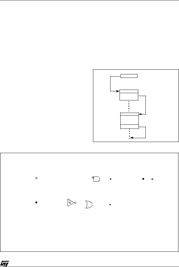
The ST62T52B and ST62T62B devices is low cost members of the ST62xx 8-bit HCMOS family of microcontrollers, which is targeted at low to medium complexity applications. All ST62xx devices are based on a building block approach: a common core is surrounded by a number of on-chip peripherals.
The ST62E62B is the erasable EPROM version of the ST62T62B device, which may be used to emulate the ST62T52B and ST62T62B devices as well as the ST6252B and ST6262B ROM devices.
OTP and EPROM devices are functionally identical. The ROM based versions offer the same functionality selecting as ROM options the options de-
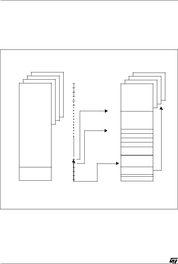
Figure 1. Block Diagram
fined in the programmable option byte of the OTP/EPROM versions.
OTP devices offer all the advantages of user programmability at low cost, which make them the ideal choice in a wide range of applications where frequent code changes, multiple code versions or last minute programmability are required.
These compact low-cost devices feature a Timer comprising an 8-bit counter and a 7-bit programmable prescaler, an 8-bit Auto-Reload Timer, EEPROM data capability (except ST62T52B), an 8-bit A/D Converter with 4 analog inputs and a Digital Watchdog timer, making them well suited for a wide range of automotive, appliance and industrial applications.
|
|
8-BIT |
PORT A |
PA4..PA5 / Ain |
|
|
A/D CONVERTER |
||
TEST/VPP |
|
|
|
|
TEST |
|
|
PB0, PB2..PB3 / 20 mA Sink |
|
|
|
|
|
|
|
|
|
PORT B |
PB6 / ARTimin / 20 mA Sink |
NMI |
INTERRUPT |
|
|
PB7 / ARTimout / 20 mA Sink |
DATA ROM |
|
|
||
|
|
|
|
|
|
|
USER |
PORT C |
PC2..PC3 / Ain |
|
|
SELECTABLE |
||
|
PROGRAM |
|
|
|
|
|
|
|
|
|
MEMORY |
|
|
|
|
1836 bytes OTP |
DATA RAM |
AUTORELOAD |
|
|
128 Bytes |
|
||
|
TIMER |
|
||
|
(ST62T52B, T62B) |
|
1836 bytes EPROM
|
|
|
|
|
|
(ST62E62B) |
|
|
|
|
|
|
|
|
|
|
|
|
|
|
|
|
|
|
|
|
|
|
|
|
|
|||||||||||||
|
|
|
|
|
|
|
|
|
|
|
|
|
|
|
|
|
|
|
|
|
|
|
DATA EEPROM |
|
|
|
|
|
|
|
TIMER |
|
||||||||||||
|
|
|
|
|
|
|
|
|
|
|
|
|
|
|
|
|
|
|
|
|
|
|
|
|
|
64 Bytes |
|
|
|
|
|
|
|
|
||||||||||
|
|
|
|
|
|
|
|
|
|
|
|
|
|
|
|
|
|
|
|
|
|
|
|
|
|
|
|
|
|
|
|
|
|
|||||||||||
|
|
|
|
|
|
|
|
|
|
|
|
|
|
|
|
|
|
|
|
|
|
|
|
(ST62T62B/E62B) |
|
|
|
|
|
|
|
|
|
|||||||||||
|
|
|
|
|
|
|
|
|
|
|
|
|
|
|
|
|
|
|
|
|
|
|
|
|
|
|
|
|
|
|
|
|
||||||||||||
|
|
|
|
|
|
|
|
|
|
|
|
|
|
|
|
|
|
|
|
|
|
|
|
|
|
|
|
|
|
|
|
|
||||||||||||
|
|
|
|
|
|
|
|
|
|
|
|
|
|
|
|
|
|
|
|
|
|
|
|
|
|
|
|
|
|
|
|
|
|
|
|
|
|
|
|
|
|
|
|
|
|
|
|
|
|
|
|
|
|
|
|
|
|
|
|
|
|
|
|
|
|
|
|
|
|
|
|
|
|
|
|
|
|
|
|
|
|
|
|
|
|
|
|
|
|
|
|
|
|
|
|
|
|
|
|
|
|
|
|
|
|
|
|
|
|
|
|
|
|
|
|
|
|
|
|
|
|
|
|
|
|
|
|
|
|
|
|
|
|
|
|
|
|
|
|
|
|
|
|
|
|
|
|
|
|
|
|
|
|
|
|
|
|
|
|
|
|
|
|
|
|
|
|
|
|
|
|
|
|
|
|
|
|
|
|
|
|
|
|
|
|
|
|
|
|
PC |
|
|
|
|
|
|
|
|
|
|
|
|
|
|
|
|
|
|
|
|
|
|
|
|
|
|
|
|
|
|
|
|
||
|
|
|
|
|
|
|
|
|
|
|
|
|
|
|
|
|
|
|
|
|
|
|
|
|
|
|
|
|
|
|
|
|
|
|
|
|
|
|
|
|
|
|
|
|
|
|
STACK LEVEL 1 |
|
|
|
|
|
|
|
|
|
|
|
|
|
|
|
|
|
|
|
|
|
|
|
|
|
|||||||||||||||||
|
|
STACK LEVEL 2 |
|
|
|
|
|
|
|
|
|
|
|
|
|
|
|
|
|
|
|
|
|
|
|
DIGITAL |
|
|||||||||||||||||
|
|
STACK LEVEL 3 |
|
|
|
|
|
8 BIT CORE |
|
|
|
|
|
|
|
WATCHDOG |
|
|||||||||||||||||||||||||||
|
|
|
|
|
|
|
|
|
|
|
|
|
|
|||||||||||||||||||||||||||||||
|
|
|
|
|
|
|
|
|
|
|
|
|
|
|||||||||||||||||||||||||||||||
|
|
STACK LEVEL 4 |
|
|
|
|
|
|
|
|
|
|
|
|
|
|
|
|
|
|
|
|
|
|
|
|
|
|||||||||||||||||
|
|
|
|
|
|
|
|
|
|
|
|
|
|
|
|
|
|
|
|
|
|
|
|
|
|
|
||||||||||||||||||
|
|
|
|
|
|
|
|
|
|
|
|
|
|
|
|
|
|
|
|
|
|
|
|
|
|
|
||||||||||||||||||
|
|
STACK LEVEL 5 |
|
|
|
|
|
|
|
|
|
|
|
|
|
|
|
|
|
|
|
|
|
|
|
|
|
|||||||||||||||||
|
|
|
|
|
|
|
|
|
|
|
|
|
|
|
|
|
|
|
|
|
|
|
|
|
|
|
|
|||||||||||||||||
|
|
STACK LEVEL 6 |
|
|
|
|
|
|
|
|
|
|
|
|
|
|
|
|
|
|
|
|
|
|
|
|
|
|||||||||||||||||
|
|
|
|
|
|
|
|
|
|
|
|
|
|
|
|
|
|
|
|
|
|
|
|
|
|
|||||||||||||||||||
|
|
|
|
|
|
|
|
|
|
|
|
|
|
|
|
|
|
|
|
|
|
|
|
|
|
|
|
|
|
|
|
|
|
|
|
|
|
|
|
|
|
|
|
|
|
|
|
|
|
|
|
|
|
|
|
|
|
|
|
|
|
|
|
|
|
|
|
|
|
|
|
|
|
|
|
|
|
|
|
|
|
|
|
|
|
|
|
||
|
POWER |
|
OSCILLATOR |
|
RESET |
|
|
|
|
|
|
|
|
|
|
|||||||||||||||||||||||||||||
|
SUPPLY |
|
|
|
|
|
|
|
|
|
|
|
|
|||||||||||||||||||||||||||||||
|
|
|
|
|
|
|
|
|
|
|
|
|
|
|
|
|
|
|
|
|
|
|
|
|
|
|
|
|
|
|
|
|
|
|||||||||||
|
|
|
|
|
|
|
|
|
|
|
|
|
|
|
|
|
|
|
|
|
|
|
|
|
|
|
|
|
|
|
|
|
|
|
|
|
|
|
|
|
|
|
|
|
|
VDD VSS OSCin OSCout |
|
|
|
|
|
|
|
|
|
|
|
|
|
||||||||||||||||||||||||||||||
|
|
|
RESET |
|
|
|
|
|
|
|
|
|
||||||||||||||||||||||||||||||||
4/68

ST62T52B ST62T62B/E62B
1.2 PIN DESCRIPTIONS
VDD and VSS. Power is supplied to the MCU via these two pins. VDD is the power connection and VSS is the ground connection.
OSCin and OSCout. These pins are internally connected to the on-chip oscillator circuit. A quartz crystal, a ceramic resonator or an external clock signal can be connected between these two pins. The OSCin pin is the input pin, the OSCout pin is the output pin.
RESET. The active-low RESET pin is used to restart the microcontroller.
TEST/VPP. The TEST must be held at VSS for normal operation. If TEST pin is connected to a +12.5V level during the reset phase, the EPROM/OTP programming Mode is entered.
NMI. The NMI pin provides the capability for asynchronous interruption, by applying an external non maskable interrupt to the MCU. The NMI input is falling edge sensitive. It is provided with an onchip pullup resistor and Schmitt trigger characteristics.
PA4-PA5. These 2 lines are organized as one I/O port (A). Each line may be configured under software control as inputs with or without internal pullup resistors, interrupt generating inputs with pullup resistors, open-drain or push-pull outputs, analog inputs for the A/D converter.
PB0, PB2-PB3, PB6-PB7. These 5 lines are organized as one I/O port (B). Each line may be configured under software control as inputs with or without internal pull-up resistors, interrupt generating inputs with pull-up resistors, open-drain or push-pull outputs. PB6/ARTIMin and PB7/ARTI-
Mout are either Port B I/O bits or the Input and Output pins of the ARTimer.
Reset state of PB2-PB3 pins can be defined by option either with pull-up or high impedance.
PB0, PB2-PB3, PB6-PB7 scan also sink 20mA for direct LED driving.
PC2-PC3. These 2 lines are organized as one I/O port (C). Each line may be configured under software control as input with or without internal pullup resistor, interrupt generating input with pull-up resistor, analog input for the A/D converter, opendrain or push-pull output.
Figure 2. ST62T52B, E62B and T62B Pin
Configuration
PB0 |
|
|
|
|
|
PC2/Ain |
|
|
1 |
16 |
|
|
|||
|
|
|
|
|
|
||
|
|
15 |
|
|
|
|
|
VPP/TEST |
|
2 |
|
|
PC3/Ain |
||
|
14 |
|
|||||
|
|
|
|
|
|
||
PB2 |
|
3 |
|
|
NMI |
||
PB3 |
|
4 |
13 |
|
|
|
|
|
|
|
RESET |
|
|||
|
|
12 |
|
|
|
|
|
ARTIMin/PB6 |
|
5 |
|
OSCout |
|||
ARTIMout/PB7 |
|
6 |
11 |
|
|
OSCin |
|
|
|
||||||
VDD |
|
7 |
10 |
|
|
PA5/Ain |
|
|
|
|
|||||
VSS |
|
8 |
9 |
|
|
PA4/Ain |
|
|
|
|
|||||
|
|
|
|||||
|
|
|
|
|
|
|
|
|
|
|
|
|
|
|
|
5/68
ST62T52B ST62T62B/E62B
1.3 MEMORY MAP
1.3.1 Introduction
The MCU operates in three separate memory spaces: Program space, Data space, and Stack space. Operation in these three memory spaces is described in the following paragraphs.
Briefly, Program space contains user program code in OTP and user vectors; Data space contains user data in RAM and in OTP, and Stack space accommodates six levels of stack for subroutine and interrupt service routine nesting.
Figure 3. Memory Addressing Diagram
PROGRAM SPACE |
|
DATA SPACE |
|
|
|
0000h |
000h |
|
|
|
|
|
|
RAM / EEPROM |
|
|
BANKING AREA |
0-63 |
03Fh |
|
|
040h |
|
|
|
DATA READ-ONLY |
PROGRAM |
|
MEMORY WINDOW |
MEMORY |
07Fh |
|
|
080h |
X REGISTER |
|
081h |
Y REGISTER |
|
082h |
V REGISTER |
|
083h |
W REGISTER |
|
084h |
RAM |
|
|
|
|
0C0h |
DATA READ-ONLY |
0FF0h |
|
MEMORY |
|
WINDOW SELECT |
|
INTERRUPT & |
|
DATA RAM |
|
BANK SELECT |
|
RESET VECTORS |
|
|
|
|
|
0FFFh |
0FFh |
ACCUMULATOR |
6/68 |
|
|

ST62T52B ST62T62B/E62B
MEMORY MAP (Cont’d)
1.3.2 Program Space
Program Space comprises the instructions to be executed, the data required for immediate addressing mode instructions, the reserved factory test area and the user vectors. Program Space is addressed via the 12-bit Program Counter register (PC register).
1.3.2.1 Program Memory Protection
The Program Memory in OTP or EPROM devices can be protected against external readout of memory by selecting the READOUT PROTECTION option in the option byte.
In the EPROM parts, READOUT PROTECTION option can be disactivated only by U.V. erasure that also results into the whole EPROM context erasure.
Note: Once the Readout Protection is activated, it is no longer possible, even for SGS-THOMSON, to gain access to the OTP contents. Returned parts with a protection set can therefore not be accepted.
Figure 4. ST62T52B/T62B Program
Memory Map
0000h
RESERVED*
087Fh
0880h
|
|
USER |
|
|
PROGRAM MEMORY |
|
|
1836 BYTES |
|
|
(OTP/EPROM) |
0F9Fh |
|
|
0FA0h |
|
RESERVED* |
0FEFh |
|
|
|
|
|
0FF0h |
|
INTERRUPT VECTORS |
0FF7h |
|
|
|
|
|
0FF8h |
|
RESERVED |
0FFBh |
|
|
|
|
|
0FFCh |
|
NMI VECTOR |
0FFDh |
|
|
|
|
|
0FFEh |
|
USER RESET VECTOR |
0FFFh |
|
|
|
|
(*) Reserved areas should be filled with 0FFh
7/68

ST62T52B ST62T62B/E62B
MEMORY MAP (Cont’d)
1.3.3 Data Space
Data Space accommodates all the data necessary for processing the user program. This space comprises the RAM resource, the processor core and peripheral registers, as well as read-only data such as constants and look-up tables in OTP/EPROM.
1.3.3.1 Data ROM
All read-only data is physically stored in program memory, which also accommodates the Program Space. The program memory consequently contains the program code to be executed, as well as the constants and look-up tables required by the application.
The Data Space locations in which the different constants and look-up tables are addressed by the processor core may be thought of as a 64-byte window through which it is possible to access the read-only data stored in OTP/EPROM.
1.3.3.2 Data RAM/EEPROM
In ST62T52B, T62B and ST62E62B devices, the data space includes 60 bytes of RAM, the accumulator (A), the indirect registers (X), (Y), the short direct registers (V), (W), the I/O port registers, the peripheral data and control registers, the interrupt option register and the Data ROM Window register (DRW register).
Additional RAM and EEPROM pages can also be addressed using banks of 64 bytes located between addresses 00h and 3Fh.
1.3.4 Stack Space
Stack space consists of six 12-bit registers which are used to stack subroutine and interrupt return addresses, as well as the current program counter contents.
Table 1. Additional RAM / EEPROM Banks
Device |
RAM |
EEPROM |
|
|
|
ST62T52B |
1 x 64 bytes |
- |
|
|
|
ST62T62B |
1 x 64 bytes |
1 x 64 bytes |
|
|
|
8/68
Table 2. ST62T52B, T62B and ST62E62B Data
Memory Space
RAM / EEPROM banks |
000h |
|
03Fh |
||
|
||
|
040h |
|
DATA ROM WINDOW AREA |
|
|
|
07Fh |
|
X REGISTER |
080h |
|
Y REGISTER |
081h |
|
V REGISTER |
082h |
|
W REGISTER |
083h |
|
DATA RAM 60 BYTES |
084h |
|
0BFh |
||
|
||
PORT A DATA REGISTER |
0C0h |
|
PORT B DATA REGISTER |
0C1h |
|
PORT C DATA REGISTER |
0C2h |
|
RESERVED |
0C3h |
|
PORT A DIRECTION REGISTER |
0C4h |
|
PORT B DIRECTION REGISTER |
0C5h |
|
PORT C DIRECTION REGISTER |
0C6h |
|
RESERVED |
0C7h |
|
INTERRUPT OPTION REGISTER |
0C8h* |
|
DATA ROM WINDOW REGISTER |
0C9h* |
|
RESERVED |
0CAh |
|
0CBh |
||
|
||
PORT A OPTION REGISTER |
0CCh |
|
PORT B OPTION REGISTER |
0CDh |
|
PORT C OPTION REGISTER |
0CEh |
|
RESERVED |
0CFh |
|
A/D DATA REGISTER |
0D0h |
|
A/D CONTROL REGISTER |
0D1h |
|
TIMER PRESCALER REGISTER |
0D2h |
|
TIMER COUNTER REGISTER |
0D3h |
|
TIMER STATUS CONTROL REGISTER |
0D4h |
|
AR TIMER MODE CONTROL REGISTER |
0D5h |
|
AR TIMER STATUS/CONTROL REGISTER1 |
0D6h |
|
AR TIMER STATUS/CONTROL REGISTER2 |
0D7h |
|
WATCHDOG REGISTER |
0D8h |
|
AR TIMER RELOAD/CAPTURE REGISTER |
0D9h |
|
AR TIMER COMPARE REGISTER |
0DAh |
|
AR TIMER LOAD REGISTER |
0DBh |
|
OSCILLATOR CONTROL REGISTER |
0DCh* |
|
MISCELLANEOUS |
0DDh |
|
RESERVED |
0DEh |
|
0E7h |
||
|
||
DATA RAM/EEPROM REGISTER |
0E8h* |
|
RESERVED |
0E9h |
|
EEPROM CONTROL REGISTER |
0EAh |
|
RESERVED |
0EBh |
|
0FEh |
||
|
||
ACCUMULATOR |
0FFh |
* WRITE ONLY REGISTER
ST62T52B ST62T62B/E62B
MEMORY MAP (Cont’d)
1.3.5 Data Window Register (DWR)
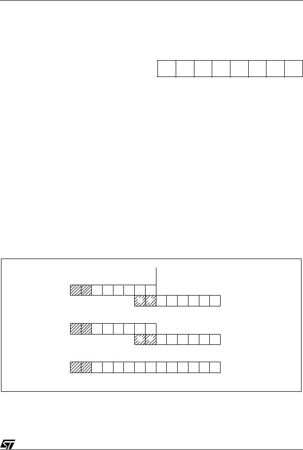
The Data read-only memory window is located from address 0040h to address 007Fh in Data space. It allows direct reading of 64 consecutive bytes located anywhere in program memory, between address 0000h and 0FFFh (top memory address depends on the specific device). All the program memory can therefore be used to store either instructions or read-only data. Indeed, the window can be moved in steps of 64 bytes along the program memory by writing the appropriate code in the Data Window Register (DWR).
The DWR can be addressed like any RAM location in the Data Space, it is however a write-only register and therefore cannot be accessed using single-bit operations. This register is used to position the 64-byte read-only data window (from address 40h to address 7Fh of the Data space) in program memory in 64-byte steps. The effective address of the byte to be read as data in program memory is obtained by concatenating the 6 least significant bits of the register address given in the instruction (as least significant bits) and the content of the DWR register (as most significant bits), as illustrated in Figure 5 below. For instance, when addressing location 0040h of the Data Space, with 0 loaded in the DWR register, the physical location addressed in program memory is 00h. The DWR register is not cleared on reset, therefore it must be written to prior to the first access to the Data read-only memory window area.
Data Window Register (DWR)
Address: 0C9h — Write Only
7 |
0 |
-- DWR5 DWR4 DWR3 DWR2 DWR1 DWR0
Bits 6, 7 = Not used.
Bit 5-0 = DWR5-DWR0: Data read-only memory Window Register Bits. These are the Data readonly memory Window bits that correspond to the upper bits of the data read-only memory space.
Caution: This register is undefined on reset. Neither read nor single bit instructions may be used to address this register.
Note: Care is required when handling the DWR register as it is write only. For this reason, the DWR contents should not be changed while executing an interrupt service routine, as the service routine cannot save and then restore the register’s previous contents. If it is impossible to avoid writing to the DWR during the interrupt service routine, an image of the register must be saved in a RAM location, and each time the program writes to the DWR, it must also write to the image register. The image register must be written first so that, if an interrupt occurs between the two instructions, the DWR is not affected.
Figure 5. Data read-only memory Window Memory Addressing
DATA ROM |
13 |
12 |
11 |
10 |
9 |
8 |
7 |
6 |
5 |
4 |
3 |
2 |
1 |
0 |
PROGRAM SPACE ADDRESS |
|
|
|
|
|
|
|
|
|
|
|
|
|
|
READ |
|
WINDOW REGISTER 7 |
6 |
5 |
4 |
3 |
2 |
1 |
0 |
|
|
|
|
|
|
||
|
|
|
|
|
|
|
|||||||||
CONTENTS |
|
|
|
|
|
|
|
|
5 |
4 |
3 |
2 |
1 |
0 |
DATA SPACE ADDRESS |
(DWR) |
|
|
|
|
|
|
|
|
|||||||
|
|
|
|
|
|
|
|
|
|
|
|
|
|
: |
|
|
|
|
|
|
|
|
0 |
1 |
|
|
|
|
|
|
40h-7Fh |
|
|
|
|
|
|
|
|
|
|
|
|
|
|
|
IN INSTRUCTION |
Example: |
|
|
|
|
|
|
|
|
|
|
|
|
|
DWR=28h |
1 |
0 |
1 |
0 |
0 |
0 |
|
|
|
|
|
|
DATA SPACE ADDRESS |
|
|
|
|
|
|
|
|
|
|
|
|
||
|
|
|
|
|
0 |
1 |
0 |
1 |
1 |
0 |
0 |
1 |
|
|
|
|
|
|
: |
||||||||
|
|
|
|
|
|
|
|
|
|
|
|
|
59h |
ROM |
1 |
0 |
1 |
0 |
0 |
0 |
0 |
1 |
1 |
0 |
0 |
1 |
|
ADDRESS:A19h |
|
||||||||||||
|
|
|
|
|
|
|
|
|
|
|
|
|
VR01573C
9/68

ST62T52B ST62T62B/E62B
MEMORY MAP (Cont’d)
1.3.6 Data RAM/EEPROM Bank Register (DRBR)
Address: E8h — Write only
7 |
|
|
|
|
|
|
0 |
|
|
|
|
|
|
|
|
|
|
- |
- |
- |
DRBR |
- |
- |
- |
DRBR |
|
4 |
0 |
|||||||
|
|
|
|
|
|
|||
|
|
|
|
|
|
|
|
Bit 7-5 = These bits are not used
Bit 4 - DRBR4. This bit, when set, selects RAM Page 2.
Bit 1-3. Not used
Bit 0. DRBR0. This bit, when set, selects EEPROM page 0.
The selection of the bank is made by programming the Data RAM Bank Switch register (DRBR register) located at address E8h of the Data Space according to Table 1. No more than one bank should be set at a time.
The DRBR register can be addressed like a RAM Data Space at the address E8h; nevertheless it is a write only register that cannot be accessed with single-bit operations. This register is used to select the desired 64-byte RAM bank of the Data Space. The number of banks has to be loaded in the DRBR register and the instruction has to point to the selected location as if it was in bank 0 (from 00h address to 3Fh address).
This register is not cleared during the MCU initialization, therefore it must be written before the first access to the Data Space bank region. Refer to
10/68
the Data Space description for additional information. The DRBR register is not modified when an interrupt or a subroutine occurs.
Notes :
Care is required when handling the DRBR register as it is write only. For this reason, it is not allowed to change the DRBR contents while executing interrupt service routine, as the service routine cannot save and then restore its previous content. If it is impossible to avoid the writing of this register in interrupt service routine, an image of this register must be saved in a RAM location, and each time the program writes to DRBR it must write also to the image register. The image register must be written first, so if an interrupt occurs between the two instructions the DRBR is not affected.
In DRBR Register, only 1 bit must be set. Otherwise two or more pages are enabled in parallel, producing errors.
Table 3. Data RAM Bank Register Set-up
DRBR |
ST62T52B |
ST62T62B |
|
|
|
00 |
None |
None |
|
|
|
01 |
Not available |
EEPROM page 0 |
|
|
|
02 |
Not Available |
Not Available |
|
|
|
08 |
Not available |
Not available |
|
|
|
10h |
RAM Page 2 |
RAM Page 2 |
|
|
|
other |
Reserved |
Reserved |
|
|
|
ST62T52B ST62T62B/E62B
MEMORY MAP (Cont’d)
1.3.7 EEPROM Description
EEPROM memory is located in 64-byte pages in data space. This memory may be used by the user program for non-volatile data storage.
Data space from 00h to 3Fh is paged as described in Table 4 . Row Arrangement for Parallel Writing of EEPROM Locations. EEPROM locations are accessed directly by addressing these paged sections of data space.
The EEPROM does not require dedicated instructions for read or write access. Once selected via the Data RAM Bank Register, the active EEPROM page is controlled by the EEPROM Control Register (EECTL), which is described below.
Bit E20FF of the EECTL register must be reset prior to any write or read access to the EEPROM. If no bank has been selected, or if E2OFF is set, any access is meaningless.
Programming must be enabled by setting the E2ENA bit of the EECTL register.
The E2BUSY bit of the EECTL register is set when the EEPROM is performing a programming cycle. Any access to the EEPROM when E2BUSY is set is meaningless.
Provided E2OFF and E2BUSY are reset, an EEPROM location is read just like any other data location, also in terms of access time.
Writing to the EEPROM may be carried out in two modes: Byte Mode (BMODE) and Parallel Mode
(PMODE). In BMODE, one byte is accessed at a time, while in PMODE up to 8 bytes in the same row are programmed simultaneously (with consequent speed and power consumption advantages, the latter being particularly important in battery powered circuits).
General Notes:
Data should be written directly to the intended address in EEPROM space. There is no buffer memory between data RAM and the EEPROM space.
When the EEPROM is busy (E2BUSY = “1”) EECTL cannot be accessed in write mode, it is only possible to read the status of E2BUSY. This implies that as long as the EEPROM is busy, it is not possible to change the status of the EEPROM Control Register. EECTL bits 4 and 5 are reserved and must never be set.
Care is required when dealing with the EECTL register, as some bits are write only. For this reason, the EECTL contents must not be altered while executing an interrupt service routine.
If it is impossible to avoid writing to this register within an interrupt service routine, an image of the register must be saved in a RAM location, and each time the program writes to EECTL it must also write to the image register. The image register must be written to first so that, if an interrupt occurs between the two instructions, the EECTL will not be affected.
Table 4. . Row Arrangement for Parallel Writing of EEPROM Locations
|
|
|
|
|
|
|
|
|
Dataspace |
|
|
|
|
|
|
|
|
|
addresses. |
|
|
|
|
|
|
|
|
|
Banks 0 and 1. |
Byte |
0 |
1 |
2 |
3 |
4 |
5 |
6 |
7 |
|
ROW7 |
|
|
|
|
|
|
|
|
38h-3Fh |
ROW6 |
|
|
|
|
|
|
|
|
30h-37h |
ROW5 |
|
|
|
|
|
|
|
|
28h-2Fh |
ROW4 |
|
|
|
|
|
|
|
|
20h-27h |
ROW3 |
|
|
|
|
|
|
|
|
18h-1Fh |
ROW2 |
|
|
|
|
|
|
|
|
10h-17h |
ROW1 |
|
|
|
|
|
|
|
|
08h-0Fh |
ROW0 |
|
|
|
|
|
|
|
|
00h-07h |
Up to 8 bytes in each row may be programmed simultaneously in Parallel Write mode.
The number of available 64-byte banks (1 or 2) is device dependent.
11/68

ST62T52B ST62T62B/E62B
MEMORY MAP (Cont’d)
Additional Notes on Parallel Mode:
If the user wishes to perform parallel programming, the first step should be to set the E2PAR2 bit. From this time on, the EEPROM will be addressed in write mode, the ROW address will be latched and it will be possible to change it only at the end of the programming cycle, or by resetting E2PAR2 without programming the EEPROM. After the ROW address is latched, the MCU can only “see” the selected EEPROM row and any attempt to write or read other rows will produce errors.
The EEPROM should not be read while E2PAR2 is set.
As soon as the E2PAR2 bit is set, the 8 volatile ROW latches are cleared. From this moment on, the user can load data in all or in part of the ROW. Setting E2PAR1 will modify the EEPROM registers corresponding to the ROW latches accessed after E2PAR2. For example, if the software sets E2PAR2 and accesses the EEPROM by writing to addresses 18h, 1Ah and 1Bh, and then sets E2PAR1, these three registers will be modified simultaneously; the remaining bytes in the row will be unaffected.
Note that E2PAR2 is internally reset at the end of the programming cycle. This implies that the user must set the E2PAR2 bit between two parallel programming cycles. Note that if the user tries to set E2PAR1 while E2PAR2 is not set, there will be no programming cycle and the E2PAR1 bit will be unaffected. Consequently, the E2PAR1 bit cannot be set if E2ENA is low. The E2PAR1 bit can be set by the user, only if the E2ENA and E2PAR2 bits are also set.
EEPROM Control Register (EECTL)
Address: EAh — Read/Write
Reset status: 00h
7 |
|
|
|
|
|
|
0 |
|
D7 |
E2O |
D5 |
D4 |
E2PA |
E2PA |
E2BU |
E2E |
|
FF |
R1 |
R2 |
SY |
NA |
||||
|
|
|
||||||
|
|
|
|
|
|
|
|
Bit 7 = D7: Unused.
Bit 6 = E2OFF: Stand-by Enable Bit. WRITE ONLY. If this bit is set the EEPROM is disabled (any access will be meaningless) and the power consumption of the EEPROM is reduced to its lowest value.
Bit 5-4 = D5-D4: Reserved. MUST be kept reset.
Bit 3 = E2PAR1: Parallel Start Bit. WRITE ONLY. Once in Parallel Mode, as soon as the user software sets the E2PAR1 bit, parallel writing of the 8 adjacent registers will start. This bit is internally reset at the end of the programming procedure. Note that less than 8 bytes can be written if required, the undefined bytes being unaffected by the parallel programming cycle; this is explained in greater detail in the Additional Notes on Parallel Mode overleaf.
Bit 2 = E2PAR2: Parallel Mode En. Bit. WRITE ONLY. This bit must be set by the user program in order to perform parallel programming. If E2PAR2 is set and the parallel start bit (E2PAR1) is reset, up to 8 adjacent bytes can be written simultaneously. These 8 adjacent bytes are considered as a row, whose address lines A7, A6, A5, A4, A3 are fixed while A2, A1 and A0 are the changing bits, as illustrated in Table 4. E2PAR2 is automatically reset at the end of any parallel programming procedure. It can be reset by the user software before starting the programming procedure, thus leaving the EEPROM registers unchanged.
Bit 1 = E2BUSY: EEPROM Busy Bit. READ ONLY. This bit is automatically set by the EEPROM control logic when the EEPROM is in programming mode. The user program should test it before any EEPROM read or write operation; any attempt to access the EEPROM while the busy bit is set will be aborted and the writing procedure in progress will be completed.
Bit 0 = E2ENA: EEPROM Enable Bit. WRITE ONLY. This bit enables programming of the EEPROM cells. It must be set before any write to the EEPROM register. Any attempt to write to the EEPROM when E2ENA is low is meaningless and will not trigger a write cycle.
12/68

ST62T52B ST62T62B/E62B
1.4 PROGRAMMING MODES
1.4.1 Option Byte
The Option Byte allows configuration capability to the MCUs. Option byte’s content is automatically read, and the selected options enabled, when the chip reset is activated.
It can only be accessed during the programming mode. This access is made either automatically (copy from a master device) or by selecting the OPTION BYTE PROGRAMMING mode of the programmer.
The option byte is located in a non-user map. No address has to be specified.
EPROM Code Option Byte
7 |
|
|
0 |
|||||
PRO- |
EXTC- |
PB2-3 |
- |
WDACT |
DELAY |
OSCIL |
- |
|
TECT |
NTL |
PULL |
||||||
|
|
|
|
|
||||
|
|
|
|
|
|
|
|
|
PROTECT. This bit allows the protection of the software contents against piracy. When the bit PROTECT is set high, readout of the OTP contents is prevented by hardware. No programming equipment is able to gain access to the user program. When this bit is low, the user program can be read.
EXTCNTL. This bit selects the External STOP Mode capability. When EXTCNTL is high, pin NMI controls if the STOP mode can be accessed when the watchdog is active. When EXTCNTL is low, the STOP instruction is processed as a WAIT as soon as the watchdog is active.
PB2-3 PULL. When set this bit removes pull-up at reset on PB2-PB3 pins. When cleared PB2-PB3 pins have an internal pull-up resistor at reset.
D4. Reserved. Must be cleared to zero.
WDACT. This bit controls the watchdog activation. When it is high, hardware activation is selected. The software activation is selected when WDACT is low.
DELAY. This bit enables the selection of the delay internally generated after pin RESET is released. When DELAY is low, the delay is 2048 cycles of
the oscillator, it is of 32768 cycles when DELAY is high.
OSCIL. When this bit is low, the oscillator must be controlled by a quartz crystal, a ceramic resonator or an external frequency. When it is high, the oscillator must be controlled by an RC network, with only the resistor having to be externally provided.
D0. Reserved. Must be cleared to zero.
The Option byte is written during programming either by using the PC menu (PC driven Mode) or automatically (stand-alone mode)
1.4.2 Program Memory
EPROM/OTP programming mode is set by a +12.5V voltage applied to the TEST/VPP pin. The programming flow of the ST62T62B is described in the User Manual of the EPROM Programming Board.
The MCUs can be programmed with the ST62E6xB EPROM programming tools available from SGS-THOMSON.
Table 5. ST62T52B/T62B Program Memory Map
Device Address |
Description |
|
|
0000h-087Fh |
Reserved |
0880h-0F9Fh |
User ROM |
0FA0h-0FEFh |
Reserved |
0FF0h-0FF7h |
Interrupt Vectors |
0FF8h-0FFBh |
Reserved |
0FFCh-0FFDh |
NMI Interrupt Vector |
0FFEh-0FFFh |
Reset Vector |
|
|
Note: OTP/EPROM devices can be programmed with the development tools available from SGS-THOMSON (ST62E6X-EPB or ST626X-KIT).
1.4.3 . EEPROM Data Memory
EEPROM data pages are supplied in the virgin state FFh. Partial or total programming of EEPROM data memory can be performed either through the application software or through an external programmer. Any SGS-THOMSON tool used for the program memory (OTP/EPROM) can also be used to program the EEPROM data memory.
13/68

ST62T52B ST62T62B/E62B
2 CENTRAL PROCESSING UNIT
2.1 INTRODUCTION
The CPU Core of ST6 devices is independent of the I/O or Memory configuration. As such, it may be thought of as an independent central processor communicating with on-chip I/O, Memory and Peripherals via internal address, data, and control buses. In-core communication is arranged as shown in Figure 6; the controller being externally linked to both the Reset and Oscillator circuits, while the core is linked to the dedicated on-chip peripherals via the serial data bus and indirectly, for interrupt purposes, through the control registers.
2.2 CPU REGISTERS
The ST6 Family CPU core features six registers and three pairs of flags available to the programmer. These are described in the following paragraphs.
Accumulator (A). The accumulator is an 8-bit general purpose register used in all arithmetic calculations, logical operations, and data manipulations. The accumulator can be addressed in Data space as a RAM location at address FFh. Thus the ST6 can manipulate the accumulator just like any other register in Data space.
Figure 6ST6 Core Block Diagram
Indirect Registers (X, Y). These two indirect registers are used as pointers to memory locations in Data space. They are used in the register-indirect addressing mode. These registers can be addressed in the data space as RAM locations at addresses 80h (X) and 81h (Y). They can also be accessed with the direct, short direct, or bit direct addressing modes. Accordingly, the ST6 instruction set can use the indirect registers as any other register of the data space.
Short Direct Registers (V, W). These two registers are used to save a byte in short direct addressing mode. They can be addressed in Data space as RAM locations at addresses 82h (V) and 83h (W). They can also be accessed using the direct and bit direct addressing modes. Thus, the ST6 instruction set can use the short direct registers as any other register of the data space.
Program Counter (PC). The program counter is a 12-bit register which contains the address of the next ROM location to be processed by the core. This ROM location may be an opcode, an operand, or the address of an operand. The 12-bit length allows the direct addressing of 4096 bytes in Program space.
|
|
0,01 TO 8MHz |
|
|
||
|
RESET |
OSCin |
|
OSCout |
|
|
|
|
|
|
|
||
|
|
|
|
INTERRUPTS |
||
|
|
CONTROLLER |
|
|
|
|
|
|
|
|
|
|
DATA SPACE |
|
|
FLAG |
CONTROL |
|
|
|
|
OPCODE |
SIGNALS |
|
DATA |
||
|
VALUES |
|
ADDRESS/READ LINE |
|
||
|
|
|
|
|||
|
|
2 |
|
|
|
RAM/EEPROM |
|
|
|
|
|
|
|
PROGRAM |
|
|
|
|
|
DATA |
ROM/EPROM |
|
|
|
ADDRESS |
|
|
|
|
|
256 |
ROM/EPROM |
||
|
|
|
|
DECODER |
|
|
|
|
|
|
|
|
|
|
|
A-DATA |
B-DATA |
|
DEDICATIONS |
|
|
|
|
|
|
|
|
|
|
|
|
|
|
ACCUMULATOR |
|
Program Counter |
|
|
|
|
|
12 |
and |
FLAGS |
|
|
|
|
|
6 LAYER STACK |
|
ALU |
|
|
|
|
|
|
|
RESULTS TO DATA SPACE (WRITE LINE) |
||
|
|
|
|
|
|
VR01811 |
14/68 |
|
|
|
|
|
|

ST62T52B ST62T62B/E62B
CPU REGISTERS (Cont’d)
However, if the program space contains more than 4096 bytes, the additional memory in program space can be addressed by using the Program Bank Switch register.
The PC value is incremented after reading the address of the current instruction. To execute relative jumps, the PC and the offset are shifted through the ALU, where they are added; the result is then shifted back into the PC. The program counter can be changed in the following ways:
-JP (Jump) instructionPC=Jump address
-CALL instructionPC= Call address
-Relative Branch Instruction.PC= PC +/- offset
-Interrupt PC=Interrupt vector
-ResetPC= Reset vector
-RET & RETI instructionsPC= Pop (stack)
-Normal instructionPC= PC + 1
Flags (C, Z). The ST6 CPU includes three pairs of flags (Carry and Zero), each pair being associated with one of the three normal modes of operation: Normal mode, Interrupt mode and Non Maskable Interrupt mode. Each pair consists of a CARRY flag and a ZERO flag. One pair (CN, ZN) is used during Normal operation, another pair is used during Interrupt mode (CI, ZI), and a third pair is used in the Non Maskable Interrupt mode (CNMI, ZNMI).
The ST6 CPU uses the pair of flags associated with the current mode: as soon as an interrupt (or a Non Maskable Interrupt) is generated, the ST6 CPU uses the Interrupt flags (resp. the NMI flags) instead of the Normal flags. When the RETI instruction is executed, the previously used set of flags is restored. It should be noted that each flag set can only be addressed in its own context (Non Maskable Interrupt, Normal Interrupt or Main routine). The flags are not cleared during context switching and thus retain their status.
The Carry flag is set when a carry or a borrow occurs during arithmetic operations; otherwise it is cleared. The Carry flag is also set to the value of the bit tested in a bit test instruction; it also participates in the rotate left instruction.
The Zero flag is set if the result of the last arithmetic or logical operation was equal to zero; otherwise it is cleared.
Switching between the three sets of flags is performed automatically when an NMI, an interrupt or a RETI instructions occurs. As the NMI mode is
automatically selected after the reset of the MCU, the ST6 core uses at first the NMI flags.
Stack. The ST6 CPU includes a true LIFO hardware stack which eliminates the need for a stack pointer. The stack consists of six separate 12-bit RAM locations that do not belong to the data space RAM area. When a subroutine call (or interrupt request) occurs, the contents of each level are shifted into the next higher level, while the content of the PC is shifted into the first level (the original contents of the sixth stack level are lost). When a subroutine or interrupt return occurs (RET or RETI instructions), the first level register is shifted back into the PC and the value of each level is popped back into the previous level. Since the accumulator, in common with all other data space registers, is not stored in this stack, management of these registers should be performed within the subroutine. The stack will remain in its “deepest” position if more than 6 nested calls or interrupts are executed, and consequently the last return address will be lost. It will also remain in its highest position if the stack is empty and a RET or RETI is executed. In this case the next instruction will be executed.
Figure 7ST6 CPU Programming Mode
l
|
|
|
|
|
|
|
|
|
|
|
|
|
|
|
|
INDEX |
|
b7 |
X REG. POINTER |
|
b0 |
|
SHORT |
||||
|
REGISTER |
|
b7 |
Y REG. POINTER |
|
b0 |
|
DIRECT |
|||||
|
|
|
|
|
|
|
|
||||||
|
|
|
|
|
|
|
ADDRESSING |
||||||
|
|
|
|
|
|
|
|
|
|
|
|
||
|
|
|
|
|
|
b7 |
V REGISTER |
|
b0 |
|
MODE |
||
|
|
|
|
|
|
|
|
|
|||||
|
|
|
|
|
|
b7 |
W REGISTER |
|
|
b0 |
|
|
|
|
|
|
|
|
|
|
|
|
|
||||
|
|
|
|
|
|
|
|
|
|
|
|
||
|
|
|
|
|
|
b7 ACCUMULATOR |
|
b0 |
|
|
|||
|
|
|
|
|
|
|
|
|
|
|
|
||
|
|
|
|
|
|
|
|
|
|||||
|
|
b11 |
PROGRAM COUNTER |
|
|
b0 |
|
|
|||||
|
|
|
|
|
|
|
|
|
|
|
|
||
|
|
|
|
|
|
|
|
|
|
|
|
|
|
|
|
|
|
|
|
SIX LEVELS |
|
|
|
|
|
||
|
|
|
|
|
|
|
|
|
|
|
|||
|
|
|
|
|
|
|
|
|
|
|
|||
|
|
|
|
|
|
|
|
|
|
|
|||
|
|
|
|
|
STACK REGISTER |
|
|
|
|
|
|||
|
|
|
|
|
|
|
|
|
|
|
|
|
|
|
|
|
|
|
|
|
|
|
|
|
|
|
|
|
|
|
|
|
|
|
|
|
|
|
|
|
|
|
|
NORMAL FLAGS |
|
|
C |
|
Z |
|
|
||||
|
|
|
|
|
|
|
|
|
|
||||
|
|
|
|
|
|
|
|
|
|||||
|
|
INTERRUPT FLAGS |
|
C |
|
Z |
|
|
|||||
|
|
NMI FLAGS |
|
|
|
|
|
|
|
||||
|
|
|
|
|
|
|
|
|
|||||
|
|
|
|
C |
|
Z |
|
|
|||||
|
|
|
|
|
|
|
|
|
|
|
|
|
VA000423 |
|
|
|
|
|
|
|
|
|
|
|
|
|
|
|
|
|
|
|
|
|
|
|
|
|
|
|
|
15/68
ST62T52B ST62T62B/E62B
3 CLOCKS, RESET, INTERRUPTS AND POWER SAVING MODES
3.1 CLOCK SYSTEM
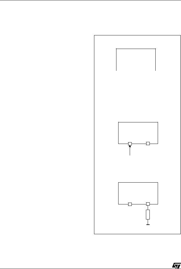
The MCU features a Main Oscillator which can be driven by an external clock, or used in conjunction with an AT-cut parallel resonant crystal or a suitable ceramic resonator, or with an external resistor (RNET).
Figure 8. illustrates various possible oscillator configurations using an external crystal or ceramic resonator, an external clock input, an external resistor
(RNET). CL1 an CL2 should have a capacitance in the range 12 to 22 pF for an oscillator frequency in the
4-8 MHz range.
Aprogrammabledivideris providedinordertoadjust the internal clock of the MCU to the best power consumption and performance trade-off.
The internal MCU clock frequency (fINT) drives directly the AR TIMER while it is divided by 12 to drive the TIMER, the A/D converter and the Watchdog timer, and by 13 to drive the CPU core, as may be seen in Figure 9..
With an 8MHz oscillator frequency, the fastest machine cycle is therefore 1.625µs.
A machine cycle is the smallest unit of time needed to execute any operation (for instance, to increment the Program Counter). An instruction may require two, four, or five machine cycles for execution.
3.1.1 Main Oscillator
The oscillator configuration may be specified by selecting the appropriate option. When the CRYSTAL/RESONATOR option is selected, it must be used with a quartz crystal, a ceramic resonator or an external signal provided on the OSCin pin. When the RC NETWORK option is selected, the system clock is generated by an external resistor.
Figure 8. Oscillator Configurations
CRYSTAL/RESONATOR CLOCK
CRYSTAL/RESONATOR option
ST6xxx
OSCin OSCout
|
|
|
|
|
|
|
|
|
|
|
|
|
|
|
|
|
CL1n |
|
|
|
|
|
|
|
|
|
|
|
|
|
C |
||
|
|
|
|
|
|
|
|
|
|
|
|
|
||||
|
|
|
|
|
|
|
|
|
|
|
|
|
||||
|
|
|
|
|
|
|
|
|
|
|
|
|
||||
|
|
|
|
|
|
|
|
|
|
|
|
|
||||
|
|
|
|
|
|
|
|
|
|
|
|
|
|
|
L2 |
|
|
|
|
|
|
|
|
|
|
|
|
|
|
|
|
|
|
EXTERNAL CLOCK
CRYSTAL/RESONATOR option
ST6xxx
OSCin OSCout
NC
RC NETWORK
RC NETWORK option
ST6xxx
OSCin OSCout
NC
RNET
16/68

ST62T52B ST62T62B/E62B
CLOCK SYSTEM (Cont’d)
Oscillator Control Registers
Address: DCh — Write only
7 |
|
|
|
|
|
0 |
||
- |
- |
- |
- |
OSCR |
OSCR |
RS1 |
RS0 |
|
3 |
2 |
|||||||
|
|
|
|
|
|
|||
|
|
|
|
|
|
|
|
|
Bit 7-4. These bits are not used.
Bit 3. Reserved. Cleared at Reset. THIS BIT MUST BE SET TO 1 BY USER PROGRAM to achieve lowest power consumption.
Bit 2. Reserved. Must be kept low.
RS1-RS0. These bits select the division ratio of the Oscillator Divider in order to generate the internal frequency. The following selctions are available:
RS1 |
RS0 |
Division Ratio |
|
|
|
0 |
0 |
1 |
0 |
1 |
2 |
1 |
0 |
4 |
1 |
1 |
4 |
|
|
|
Figure 9. Clock Circuit Block Diagram
Note: Care is required when handling the OSCR register as some bits are write only. For this reason, it is not allowed to change the OSCR contents while executing interrupt service routine, as the service routine cannot save and then restore its previous content. If it is impossible to avoid the writing of this register in interrupt service routine, an image of this register must be saved in a RAM location, and each time the program writes to OSCR it must write also to the image register. The image register must be written first, so if an interrupt occurs between the two instructions the OSCR is not affected.
fOSC |
|
|
|
POR |
|
|
|
|
|
OSCin |
fOSC |
|
: 13 |
Core |
|
|
|
||
|
|
|
|
|
|
|
|
|
Timer |
MAIN |
OSCILLATOR |
fINT |
: 12 |
Watchdog |
OSCILLATOR |
DIVIDER |
|
|
|
|
|
|
||
|
|
|
|
|
|
|
|
|
ADC |
OSCout |
|
|
: 1 |
AR Timer |
|
|
|
|
|
|
RS0, RS1 |
|
|
|
17/68
ST62T52B ST62T62B/E62B
3.2 RESETS
The MCU can be reset in three ways:
–by the external Reset input being pulled low;
–by Power-on Reset;
–by the digital Watchdog peripheral timing out.
3.2.1 RESET Input
The RESET pin may be connected to a device of the application board in order to reset the MCU if required. The RESET pin may be pulled low in RUN, WAIT or STOP mode. This input can be used to reset the MCU internal state and ensure a correct start-up procedure. The pin is active low and features a Schmitt trigger input. The internal Reset signal is generated by adding a delay to the external signal. Therefore even short pulses on the RESET pin are acceptable, provided VDD has completed its rising phase and that the oscillator is running correctly (normal RUN or WAIT modes). The MCU is kept in the Reset state as long as the RESET pin is held low.
If RESET activation occurs in the RUN or WAIT modes, processing of the user program is stopped (RUN mode only), the Inputs and Outputs are configured as inputs with pull-up resistors and the main Oscillator is restarted. When the level on the RESET pin then goes high, the initialization sequence is executed following expiry of the internal delay period.
If RESET pin activation occurs in the STOP mode, the oscillator starts up and all Inputs and Outputs are configured as inputs with pull-up resistors. When the level of the RESET pin then goes high, the initialization sequence is executed following expiry of the internal delay period.
3.2.2 Power-on Reset
The function of the POR circuit consists in waking up the MCU at an appropriate stage during the power-on sequence. At the beginning of this sequence, the MCU is configured in the Reset state: all I/O ports are configured as inputs with pull-up resistors and no instruction is executed. When the power supply voltage rises to a sufficient level, the oscillator starts to operate, whereupon an internal delay is initiated, in order to allow the oscillator to fully stabilize before executing the first instruction. The initialization sequence is executed immediately following the internal delay.
The internal delay is generated by an on-chip counter. The internal reset line is released 2048 internal clock cycles after release of the external reset.
Notes:
To ensure correct start-up, the user should take care that the reset signal is not released before the VDD level is sufficient to allow MCU operation at the chosen frequency (see Recommended Operating Conditions).
A proper reset signal for a slow rising VDD supply can generally be provided by an external RC network connected to the RESET pin.
Figure 10. Reset and Interrupt Processing
RESET |
NMI MASK SET |
INT LATCH CLEARED |
( IF PRESENT ) |
SELECT |
NMI MODE FLAGS |
PUT FFEH |
ON ADDRESS BUS |
YES |
IS RESET STILL |
PRESENT? |
NO |
LOAD PC
FROM RESET LOCATIONS
FFE/FFF
FETCH INSTRUCTION
VA000427
18/68
ST62T52B ST62T62B/E62B
RESETS (Cont’d)
3.2.3 Watchdog Reset
The MCU provides a Watchdog timer function in order to ensure graceful recovery from software upsets. If the Watchdog register is not refreshed before an end-of-count condition is reached, the internal reset will be activated. This, amongst other things, resets the watchdog counter.
The MCU restarts just as though the Reset had been generated by the RESET pin, including the built-in stabilisation delay period.
3.2.4 Application Notes
No external resistor is required between VDD and the Reset pin, thanks to the built-in pull-up device.
The POR circuit operates dynamically, in that it triggers MCU initialization on detecting the rising edge of VDD. The typical threshold is in the region of 2 volts, but the actual value of the detected threshold depends on the way in which VDD rises.
The POR circuit is NOT designed to supervise static, or slowly rising or falling VDD.
3.2.5 MCU Initialization Sequence
When a reset occurs the stack is reset, the PC is loaded with the address of the Reset Vector (located in program ROM starting at address 0FFEh). A jump to the beginning of the user program must be coded at this address. Following a
Figure 12. Reset Block Diagram
Reset, the Interrupt flag is automatically set, so that the CPU is in Non Maskable Interrupt mode; this prevents the initialisation routine from being interrupted. The initialisation routine should therefore be terminated by a RETI instruction, in order to revert to normal mode and enable interrupts. If no pending interrupt is present at the end of the initialisation routine, the MCU will continue by processing the instruction immediately following the RETI instruction. If, however, a pending interrupt is present, it will be serviced.
Figure 11. Reset and Interrupt Processing
RESET
JP |
JP:2 BYTES/4 CYCLES |
RESET
VECTOR
INITIALIZATION |
|
ROUTINE |
RETI: 1 BYTE/2 CYCLES |
|
|
|
RETI |
VA00181
|
|
|
|
|
|
|
|
|
|
|
|
|
|
|
|
|
|
|
|
|
|
|
|
|
|
|
|
|
|
|
VDD |
|
|
|
|
|
|
|
|
|
ST6 |
||||||||||||
|
|
|
|
|
|
|
|
|
|
|
|
|
||||||||||||||
|
|
|
|
|
|
|
|
|
fOSC |
|
|
|
|
|
|
CK |
|
|
||||||||
|
|
|
|
|
|
|
|
|
|
|
|
|
|
|
|
|
INTERNAL |
|||||||||
|
|
|
|
|
|
|
300kΩ |
|
|
|
|
|
|
|
COUNTER |
|
|
RESET |
||||||||
|
|
|
|
|
|
|
|
|
|
|
|
|
|
|
|
|||||||||||
|
|
|
|
|
|
|
|
|
|
|
|
|
|
|
|
|||||||||||
|
|
|
|
|
|
|
|
|
|
|
|
|
|
|
|
|
|
|
|
RESET |
RESET |
|
|
|
||
|
|
|
|
|
|
|
|
|
|
|
|
|
|
|
|
|
|
|
|
|
|
|
||||
|
RESET |
|
|
|
|
|
|
|
|
|
|
|
|
|
|
|
|
|
|
|
|
|
||||
|
|
|
|
|
|
|
|
2.8kΩ |
|
|
|
|
|
|
|
|
|
|
|
|
||||||
|
|
|
|
|
|
|
POWER ON RESET |
|
|
|
|
|
|
|
|
|
|
|
|
|
||||||
|
|
|
|
|
|
|
|
|
|
|
|
|
|
|
|
|
|
|
|
|||||||
|
|
|
|
|
|
|
WATCHDOG RESET |
|
|
|
|
|
|
|
|
|
|
|
VA0200B |
|||||||
|
|
|
|
|
|
|
|
|
|
|
|
|
|
|
|
|
|
|||||||||
|
|
|
|
|
|
|
|
|
|
|
|
|
|
|
|
|
|
|
|
|
|
|
|
|
|
|
|
|
|
|
|
|
|
|
|
|
|
|
|
|
|
|
|
|
|
|
|
|
|
|
|
||
19/68

ST62T52B ST62T62B/E62B
RESETS (Cont’d)
Table 6. Register Reset Status
Register |
Address(es) |
Status |
Comment |
|
|
|
|
Oscillator Control Register |
0DCh |
|
fINT = fOSC; user must set bit3 to 1 |
EEPROM Control Register |
0EAh |
|
EEPROM enabled (if available) |
Port Data Registers |
0C0h to 0C2h |
|
I/O are Input with pull-up |
Port Direction Register |
0C4h to 0C6h |
|
I/O are Input with pull-up |
Port Option Register |
0CCh to 0CEh |
|
I/O are Input with pull-up |
Interrupt Option Register |
0C8h |
|
Interrupt disabled |
TIMER Status/Control |
0D4h |
00h |
TIMER disabled |
AR TIMER Mode Control Register |
0D5h |
|
AR TIMER stopped |
AR TIMER Status/Control 1 Register |
0D6h |
|
|
AR TIMER Status/Control 2Register |
0D7h |
|
|
AR TIMER Compare Register |
0DAh |
|
|
Miscellaneous Register |
0DDh |
|
|
|
|
|
|
X, Y, V, W, Register |
080H TO 083H |
|
|
Accumulator |
0FFh |
|
|
Data RAM |
084h to 0BFh |
|
|
Data RAM Page REgister |
0E8h |
|
|
Data ROM Window Register |
0C9h |
Undefined |
|
EEPROM |
00h to F3h |
|
As written if programmed |
A/D Result Register |
0D0h |
|
|
AR TIMER Load Register |
0DBh |
|
|
AR TIMER Reload/Capture Register |
0D9h |
|
|
|
|
|
|
TIMER Counter Register |
0D3h |
FFh |
|
TIMER Prescaler Register |
0D2h |
7Fh |
Max count loaded |
Watchdog Counter Register |
0D8h |
FEh |
|
A/D Control Register |
0D1h |
40h |
A/D in Standby |
|
|
|
|
20/68
ST62T52B ST62T62B/E62B
3.3 DIGITAL WATCHDOG
The digital Watchdog consists of a reloadable downcounter timer which can be used to provide controlled recovery from software upsets.
The Watchdog circuit generates a Reset when the downcounter reaches zero. User software can prevent this reset by reloading the counter, and should therefore be written so that the counter is regularly reloaded while the user program runs correctly. In the event of a software mishap (usually caused by externally generated interference), the user program will no longer behave in its usual fashion and the timer register will thus not be reloaded periodically. Consequently the timer will decrement down to 00h and reset the MCU. In order to maximise the effectiveness of the Watchdog function, user software must be written with this concept in mind.
Watchdog behaviour is governed by two options, known as “WATCHDOG ACTIVATION” (i.e. HARDWARE or SOFTWARE) and “EXTERNAL STOP MODE CONTROL” (see Table 7 Recommended Option Choices).
In the SOFTWARE option, the Watchdog is disabled until bit C of the DWDR register has been set.
Table 7. Recommended Option Choices
When the Watchdog is disabled, low power Stop mode is available. Once activated, the Watchdog cannot be disabled, except by resetting the MCU.
In the HARDWARE option, the Watchdog is permanently enabled. Since the oscillator will run continuously, low power mode is not available. The STOP instruction is interpreted as a WAIT instruction, and the Watchdog continues to countdown.
However, when the EXTERNAL STOP MODE CONTROL option has been selected low power consumption may be achieved in Stop Mode.
Execution of the STOP instruction is then governed by a secondary function associated with the NMI pin. If a STOP instruction is encountered when the NMI pin is low, it is interpreted as WAIT, as described above. If, however, the STOP instruction is encountered when the NMI pin is high, the Watchdog counter is frozen and the CPU enters STOP mode.
When the MCU exits STOP mode (i.e. when an interrupt is generated), the Watchdog resumes its activity.
Functions Required |
Recommended Options |
Stop Mode & Watchdog |
“EXTERNAL STOP MODE” & “HARDWARE WATCHDOG” |
|
|
Stop Mode |
“SOFTWARE WATCHDOG” |
|
|
Watchdog |
“HARDWARE WATCHDOG” |
|
|
21/68
 Loading...