


SGS Thomson Microelectronics ST62T30BM6, ST62T30BM3, ST62T30BB6, ST62T30BB3, ST62P30BM6 Datasheet
...ST62T30B
ST62E30B
8-BIT OTP/EPROM MCUs WITH A/D CONVERTER, 16-BIT AUTO-RELOAD TIMER, EEPROM, SPI AND UART
■3.0 to 6.0V Supply Operating Range
■8 MHz Maximum Clock Frequency
■-40 to +125°C Operating Temperature Range
■Run, Wait and Stop Modes
■5 Interrupt Vectors
■Look-up Table capability in Program Memory
■Data Storage in Program Memory: User selectable size
■Data RAM: 192 bytes
■Data EEPROM: 128 bytes
■User Programmable Options
■20 I/O pins, fully programmable as:
±Input with pull-up resistor
±Input without pull-up resistor
±Input with interrupt generation
±Open-drain or push-pull output
±Analog Input
■4 I/O lines can sink up to 20mA to drive LEDs or TRIACs directly
■8-bit Timer/ Counter with 7-bit programmable prescaler
■16-bit Auto-reload Timer with 7-bit programmable prescaler (AR Timer)
■Digital Watchdog
■8-bit A/D Converter with 16 analog inputs
■8-bit Synchronous Peripheral Interface (SPI)
■8-bit Asynchronous Peripheral Interface (UART)
■On-chip Clock oscillator can be driven by Quartz Crystal or Ceramic resonator
■Oscillator Safe Guard
■One external Non-Maskable Interrupt
■ST623x-EMU2 Emulation and Development System (connects to an MS-DOS PC via a parallel port).
DEVICE SUMMARY
DEVICE |
OTP |
EPROM |
I/O Pins |
|
(Bytes) |
(Bytes) |
|||
|
|
|||
ST62T30B |
7948 |
- |
20 |
|
ST62E30B |
|
7948 |
20 |
PDIP28
PS028
CDIP28W
(See end of Datasheet for Ordering Information)
Rev. 2.5
September 1998 |
1/86 |

Table of Contents
Document
Page
ST62T30B/ST62E30B . . . . . . . . . . . . . . . . . . . . . . . . . . . . . . . . .1
1 GENERAL DESCRIPTION . . . . . . . . . . . . . . . . . . . . . . . . . . . . . . . . . . . . . . . . . . . . . . . . . . . . . .5
1.1 INTRODUCTION . . . . . . . . . . . . . . . . . . . . . . . . . . . . . . . . . . . . . . . . . . . . . . . . . . . . . . . . .5
1.2 PIN DESCRIPTIONS . . . . . . . . . . . . . . . . . . . . . . . . . . . . . . . . . . . . . . . . . . . . . . . . . . . . . .7
1.3 MEMORY MAP . . . . . . . . . . . . . . . . . . . . . . . . . . . . . . . . . . . . . . . . . . . . . . . . . . . . . . . . . .8
1.3.1 Introduction . . . . . . . . . . . . . . . . . . . . . . . . . . . . . . . . . . . . . . . . . . . . . . . . . . . . . . . .8
1.3.2 Program Space . . . . . . . . . . . . . . . . . . . . . . . . . . . . . . . . . . . . . . . . . . . . . . . . . . . . .8
1.3.3 Data Space . . . . . . . . . . . . . . . . . . . . . . . . . . . . . . . . . . . . . . . . . . . . . . . . . . . . . . .10
1.3.4 Stack Space . . . . . . . . . . . . . . . . . . . . . . . . . . . . . . . . . . . . . . . . . . . . . . . . . . . . . . .10
1.3.5 Data Window Register (DWR) . . . . . . . . . . . . . . . . . . . . . . . . . . . . . . . . . . . . . . . . . 11
1.3.6 Data RAM/EEPROM Bank Register (DRBR). . . . . . . . . . . . . . . . . . . . . . . . . . . . . . 12
1.3.7 EEPROM Description . . . . . . . . . . . . . . . . . . . . . . . . . . . . . . . . . . . . . . . . . . . . . . . 13
1.4 PROGRAMMING MODES . . . . . . . . . . . . . . . . . . . . . . . . . . . . . . . . . . . . . . . . . . . . . . . . .15
1.4.1 Option Byte . . . . . . . . . . . . . . . . . . . . . . . . . . . . . . . . . . . . . . . . . . . . . . . . . . . . . . .15
1.4.2 Program Memory . . . . . . . . . . . . . . . . . . . . . . . . . . . . . . . . . . . . . . . . . . . . . . . . . . .15
1.4.3 EEPROM Data Memory . . . . . . . . . . . . . . . . . . . . . . . . . . . . . . . . . . . . . . . . . . . . . . 15
1.4.4 EPROM Erasing . . . . . . . . . . . . . . . . . . . . . . . . . . . . . . . . . . . . . . . . . . . . . . . . . . . .15
2 CENTRAL PROCESSING UNIT . . . . . . . . . . . . . . . . . . . . . . . . . . . . . . . . . . . . . . . . . . . . . . . . .16
2.1 INTRODUCTION . . . . . . . . . . . . . . . . . . . . . . . . . . . . . . . . . . . . . . . . . . . . . . . . . . . . . . . .16
2.2 CPU REGISTERS . . . . . . . . . . . . . . . . . . . . . . . . . . . . . . . . . . . . . . . . . . . . . . . . . . . . . . .16
3 CLOCKS, RESET, INTERRUPTS AND POWER SAVING MODES . . . . . . . . . . . . . . . . . . . . . 18
3.1 CLOCK SYSTEM . . . . . . . . . . . . . . . . . . . . . . . . . . . . . . . . . . . . . . . . . . . . . . . . . . . . . . . .18
3.1.1 Main Oscillator . . . . . . . . . . . . . . . . . . . . . . . . . . . . . . . . . . . . . . . . . . . . . . . . . . . . .18
3.1.2 Low Frequency Auxiliary Oscillator (LFAO) . . . . . . . . . . . . . . . . . . . . . . . . . . . . . . . 19
3.1.3 Oscillator Safe Guard . . . . . . . . . . . . . . . . . . . . . . . . . . . . . . . . . . . . . . . . . . . . . . . . 19
3.2 RESETS . . . . . . . . . . . . . . . . . . . . . . . . . . . . . . . . . . . . . . . . . . . . . . . . . . . . . . . . . . . . . . .22
3.2.1 RESET Input . . . . . . . . . . . . . . . . . . . . . . . . . . . . . . . . . . . . . . . . . . . . . . . . . . . . . .22
3.2.2 Power-on Reset . . . . . . . . . . . . . . . . . . . . . . . . . . . . . . . . . . . . . . . . . . . . . . . . . . . .22
3.2.3 Watchdog Reset . . . . . . . . . . . . . . . . . . . . . . . . . . . . . . . . . . . . . . . . . . . . . . . . . . .23
3.2.4 Application Notes . . . . . . . . . . . . . . . . . . . . . . . . . . . . . . . . . . . . . . . . . . . . . . . . . . .23
3.2.5 MCU Initialization Sequence . . . . . . . . . . . . . . . . . . . . . . . . . . . . . . . . . . . . . . . . . . 23
3.3 DIGITAL WATCHDOG . . . . . . . . . . . . . . . . . . . . . . . . . . . . . . . . . . . . . . . . . . . . . . . . . . . .25
3.3.1 Digital Watchdog Register (DWDR) . . . . . . . . . . . . . . . . . . . . . . . . . . . . . . . . . . . . . 27
3.3.2 Application Notes . . . . . . . . . . . . . . . . . . . . . . . . . . . . . . . . . . . . . . . . . . . . . . . . . . .27
3.4 INTERRUPTS . . . . . . . . . . . . . . . . . . . . . . . . . . . . . . . . . . . . . . . . . . . . . . . . . . . . . . . . . .29
3.4.1 Interrupt request . . . . . . . . . . . . . . . . . . . . . . . . . . . . . . . . . . . . . . . . . . . . . . . . . . . .29 3.4.2 Interrupt Procedure . . . . . . . . . . . . . . . . . . . . . . . . . . . . . . . . . . . . . . . . . . . . . . . . . 30 3.4.3 Interrupt Option Register (IOR) . . . . . . . . . . . . . . . . . . . . . . . . . . . . . . . . . . . . . . . . 31 3.4.4 Interrupt sources . . . . . . . . . . . . . . . . . . . . . . . . . . . . . . . . . . . . . . . . . . . . . . . . . . .31 3.5 POWER SAVING MODES . . . . . . . . . . . . . . . . . . . . . . . . . . . . . . . . . . . . . . . . . . . . . . . . .34
3.5.1 WAIT Mode . . . . . . . . . . . . . . . . . . . . . . . . . . . . . . . . . . . . . . . . . . . . . . . . . . . . . . .34 3.5.2 STOP Mode . . . . . . . . . . . . . . . . . . . . . . . . . . . . . . . . . . . . . . . . . . . . . . . . . . . . . . .34 3.5.3 Exit from WAIT and STOP Modes . . . . . . . . . . . . . . . . . . . . . . . . . . . . . . . . . . . . . . 35
4 ON-CHIP PERIPHERALS . . . . . . . . . . . . . . . . . . . . . . . . . . . . . . . . . . . . . . . . . . . . . . . . . . . . . .36
86
4.1 I/O PORTS . . . . . . . . . . . . . . . . . . . . . . . . . . . . . . . . . . . . . . . . . . . . . . . . . . . . . . . . . . . . .36 4.1.1 Operating Modes . . . . . . . . . . . . . . . . . . . . . . . . . . . . . . . . . . . . . . . . . . . . . . . . . . .37
2/86

Table of Contents
Document
Page
4.1.2 Safe I/O State Switching Sequence . . . . . . . . . . . . . . . . . . . . . . . . . . . . . . . . . . . . . 38 4.1.3 ARTimer alternate functions . . . . . . . . . . . . . . . . . . . . . . . . . . . . . . . . . . . . . . . . . . 40 4.1.4 SPI alternate functions . . . . . . . . . . . . . . . . . . . . . . . . . . . . . . . . . . . . . . . . . . . . . . . 40 4.1.5 UART alternate functions . . . . . . . . . . . . . . . . . . . . . . . . . . . . . . . . . . . . . . . . . . . . . 40 4.1.6 I/O Port Option Registers . . . . . . . . . . . . . . . . . . . . . . . . . . . . . . . . . . . . . . . . . . . . . 42 4.1.7 I/O Port Data Direction Registers . . . . . . . . . . . . . . . . . . . . . . . . . . . . . . . . . . . . . . . 42 4.1.8 I/O Port Data Registers . . . . . . . . . . . . . . . . . . . . . . . . . . . . . . . . . . . . . . . . . . . . . . 42
4.2 TIMER . . . . . . . . . . . . . . . . . . . . . . . . . . . . . . . . . . . . . . . . . . . . . . . . . . . . . . . . . . . . . . . .43
4.2.1 Timer Operating Modes . . . . . . . . . . . . . . . . . . . . . . . . . . . . . . . . . . . . . . . . . . . . . . 44
4.2.2 Timer Interrupt . . . . . . . . . . . . . . . . . . . . . . . . . . . . . . . . . . . . . . . . . . . . . . . . . . . . .44
4.2.3 Application Notes . . . . . . . . . . . . . . . . . . . . . . . . . . . . . . . . . . . . . . . . . . . . . . . . . . .45
4.2.4 Timer Registers . . . . . . . . . . . . . . . . . . . . . . . . . . . . . . . . . . . . . . . . . . . . . . . . . . . .45
4.3 ARTIMER 16 . . . . . . . . . . . . . . . . . . . . . . . . . . . . . . . . . . . . . . . . . . . . . . . . . . . . . . . . . . .46
4.3.1 CENTRAL COUNTER . . . . . . . . . . . . . . . . . . . . . . . . . . . . . . . . . . . . . . . . . . . . . . . 47 4.3.2 SIGNAL GENERATION MODES . . . . . . . . . . . . . . . . . . . . . . . . . . . . . . . . . . . . . . . 48 4.3.3 TIMINGS MEASUREMENT MODES . . . . . . . . . . . . . . . . . . . . . . . . . . . . . . . . . . . . 50 4.3.4 INTERRUPT CAPABILITIES . . . . . . . . . . . . . . . . . . . . . . . . . . . . . . . . . . . . . . . . . . 52 4.3.5 CONTROL REGISTERS . . . . . . . . . . . . . . . . . . . . . . . . . . . . . . . . . . . . . . . . . . . . . 53 4.3.6 16-BIT REGISTERS . . . . . . . . . . . . . . . . . . . . . . . . . . . . . . . . . . . . . . . . . . . . . . . .55
4.4 A/D CONVERTER (ADC) . . . . . . . . . . . . . . . . . . . . . . . . . . . . . . . . . . . . . . . . . . . . . . . . . 57
4.4.1 Application Notes . . . . . . . . . . . . . . . . . . . . . . . . . . . . . . . . . . . . . . . . . . . . . . . . . . .57 4.5 U. A. R. T. (UNIVERSAL ASYNCHRONOUS RECEIVER/TRANSMITTER). . . . . . . . . . . 59
4.5.1 PORTS INTERFACING . . . . . . . . . . . . . . . . . . . . . . . . . . . . . . . . . . . . . . . . . . . . . . 59 4.5.2 CLOCK GENERATION . . . . . . . . . . . . . . . . . . . . . . . . . . . . . . . . . . . . . . . . . . . . . . 60 4.5.3 DATA TRANSMISSION . . . . . . . . . . . . . . . . . . . . . . . . . . . . . . . . . . . . . . . . . . . . . . 60 4.5.4 DATA RECEPTION . . . . . . . . . . . . . . . . . . . . . . . . . . . . . . . . . . . . . . . . . . . . . . . . .61 4.5.5 INTERRUPT CAPABILITIES . . . . . . . . . . . . . . . . . . . . . . . . . . . . . . . . . . . . . . . . . . 61 4.5.6 REGISTERS . . . . . . . . . . . . . . . . . . . . . . . . . . . . . . . . . . . . . . . . . . . . . . . . . . . . . .61
4.6 SERIAL PERIPHERAL INTERFACE (SPI) . . . . . . . . . . . . . . . . . . . . . . . . . . . . . . . . . . . . 63
5 SOFTWARE . . . . . . . . . . . . . . . . . . . . . . . . . . . . . . . . . . . . . . . . . . . . . . . . . . . . . . . . . . . . . . . .65
5.1 ST6 ARCHITECTURE . . . . . . . . . . . . . . . . . . . . . . . . . . . . . . . . . . . . . . . . . . . . . . . . . . . .65 5.2 ADDRESSING MODES . . . . . . . . . . . . . . . . . . . . . . . . . . . . . . . . . . . . . . . . . . . . . . . . . . .65 5.3 INSTRUCTION SET . . . . . . . . . . . . . . . . . . . . . . . . . . . . . . . . . . . . . . . . . . . . . . . . . . . . . .66
6 ELECTRICAL CHARACTERISTICS . . . . . . . . . . . . . . . . . . . . . . . . . . . . . . . . . . . . . . . . . . . . . . 71
6.1 ABSOLUTE MAXIMUM RATINGS . . . . . . . . . . . . . . . . . . . . . . . . . . . . . . . . . . . . . . . . . . . 71 6.2 RECOMMENDED OPERATING CONDITIONS. . . . . . . . . . . . . . . . . . . . . . . . . . . . . . . . . 72 6.3 DC ELECTRICAL CHARACTERISTICS . . . . . . . . . . . . . . . . . . . . . . . . . . . . . . . . . . . . . . 73 6.4 AC ELECTRICAL CHARACTERISTICS . . . . . . . . . . . . . . . . . . . . . . . . . . . . . . . . . . . . . . 74 6.5 A/D CONVERTER CHARACTERISTICS . . . . . . . . . . . . . . . . . . . . . . . . . . . . . . . . . . . . . . 74 6.6 TIMER CHARACTERISTICS . . . . . . . . . . . . . . . . . . . . . . . . . . . . . . . . . . . . . . . . . . . . . . . 75 6.7 .SPI CHARACTERISTICS . . . . . . . . . . . . . . . . . . . . . . . . . . . . . . . . . . . . . . . . . . . . . . . . .75 6.8 ARTIMER16 ELECTRICAL CHARACTERISTICS . . . . . . . . . . . . . . . . . . . . . . . . . . . . . . . 75
7 GENERAL INFORMATION . . . . . . . . . . . . . . . . . . . . . . . . . . . . . . . . . . . . . . . . . . . . . . . . . . . . .76
7.1 PACKAGE MECHANICAL DATA . . . . . . . . . . . . . . . . . . . . . . . . . . . . . . . . . . . . . . . . . . . . 76 7.2 .ORDERING INFORMATION . . . . . . . . . . . . . . . . . . . . . . . . . . . . . . . . . . . . . . . . . . . . . . . 77
3/86

Table of Contents
Document
Page
ST62P30B . . . . . . . . . . . . . . . . . . . . . . . . . . . . . . . . . . . . . . . . .79
1 GENERAL DESCRIPTION . . . . . . . . . . . . . . . . . . . . . . . . . . . . . . . . . . . . . . . . . . . . . . . . . . . . .80
1.1 INTRODUCTION . . . . . . . . . . . . . . . . . . . . . . . . . . . . . . . . . . . . . . . . . . . . . . . . . . . . . . . .80
1.2 ORDERING INFORMATION . . . . . . . . . . . . . . . . . . . . . . . . . . . . . . . . . . . . . . . . . . . . . . . 80
1.2.1 Transfer of Customer Code . . . . . . . . . . . . . . . . . . . . . . . . . . . . . . . . . . . . . . . . . . . 80 1.2.2 Listing Generation and Verification . . . . . . . . . . . . . . . . . . . . . . . . . . . . . . . . . . . . . 80
ST6230B . . . . . . . . . . . . . . . . . . . . . . . . . . . . . . . . . . . . . . . . . . .83
1 GENERAL DESCRIPTION . . . . . . . . . . . . . . . . . . . . . . . . . . . . . . . . . . . . . . . . . . . . . . . . . . . . .84
1.1 INTRODUCTION . . . . . . . . . . . . . . . . . . . . . . . . . . . . . . . . . . . . . . . . . . . . . . . . . . . . . . . .84
1.2 ROM READOUT PROTECTION . . . . . . . . . . . . . . . . . . . . . . . . . . . . . . . . . . . . . . . . . . . . 84
1.3 ORDERING INFORMATION . . . . . . . . . . . . . . . . . . . . . . . . . . . . . . . . . . . . . . . . . . . . . . . 86
1.3.1 Transfer of Customer Code . . . . . . . . . . . . . . . . . . . . . . . . . . . . . . . . . . . . . . . . . . . 86 1.3.2 Listing Generation and Verification . . . . . . . . . . . . . . . . . . . . . . . . . . . . . . . . . . . . . 86
86
4/86
ST62T30B ST62E30B
1 GENERAL DESCRIPTION
1.1 INTRODUCTION
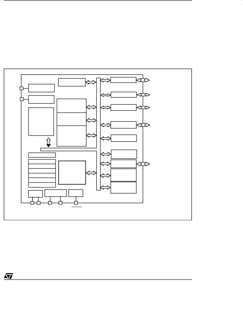
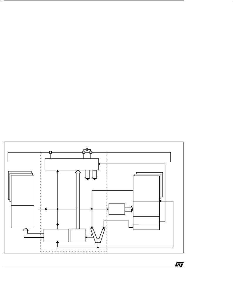
The ST62T30B and ST62E30B devices are low cost members of the ST62xx 8-bit HCMOS family of microcontrollers, which is targeted at low to medium complexity applications. All ST62xx devices are based on a building block approach: a com-
Figure 1. Block Diagram
TEST/VPP
NMI
TEST
INTERRUP T
PROGRAM
Memory
7948 bytes
PC
STACK LEVEL 1 STACK LEVEL 2 STACK LEVEL 3 STACK LEVEL 4 STACK LEVEL 5 STACK LEVEL 6
8-BIT
A/D CONVERTE R
DATA ROM
USER
SELECTA BLE
DATA RAM
192 Bytes
DATA EEPROM
128 Bytes
8 BIT CORE
POWER OSCILLATOR RESET SUPPLY
mon core is surrounded by a number of on-chip peripherals.
The ST62E30B is the erasable EPROM version of the ST62T30B device, which may be used to emulate the ST62T30B device, as well as the respective ST6230B ROM devices.
|
PA0..PA1 / 20 mA Sink |
|
|
PA2/OVF/ 20 mA Sink |
|
PORT A |
PA3/PWM/20 mA Sink |
|
PA4/Ain/CP1 |
||
|
||
|
PA5/Ain/CP2 |
|
PORT B |
PB4..PB6/Ain |
|
PORT C |
PC4..PC7/Ain |
|
|
PD1/Ain/Scl |
|
|
PD2/Ain/Sin |
|
PORT D |
PD3/Ain/Sout |
|
|
PD4/Ain/RXD1 |
|
|
PD5/Ain/TXD1 |
|
UART |
PD6,PD7/Ain |
|
|
AUTORELOAD
TIMER
TIMER |
TIMER |
SPI (SERIAL
PERIPHERAL
INTERFAC E)
DIGITAL
WATCHDOG
VDD VSS OSCin OSCout RESET
VR01823F
(VPP on EPROM/OTP versions only)
5/86
ST62T30B ST62E30B
INTRODUCTION (Cont'd)
OTP and EPROM devices are functionally identical. The ROM based versions offer the same functionality selecting as ROM options the options defined in the programmable option byte of the OTP/EPROM versions.OTP devices offer all the advantages of user programmability at low cost, which make them the ideal choice in a wide range of applications where frequent code changes, multiple code versions or last minute programmability are required.
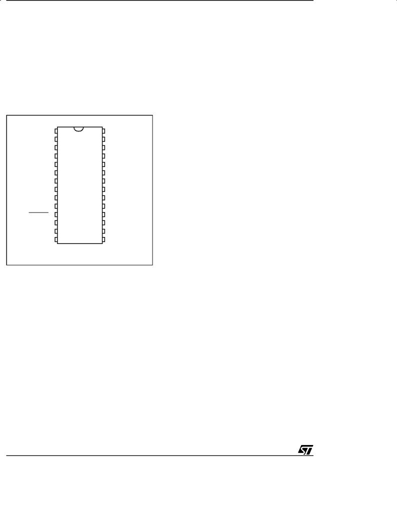
Figure 2. ST62T30B/E30B Pin Configuration
VDD |
1 |
28 |
VSS |
TIMER |
2 |
27 |
PA0 |
OSCin |
3 |
26 |
PA1 |
OSCout |
4 |
25 |
PA2/OVF |
NMI |
5 |
24 |
PA3/PWM |
Ain/PC7 |
6 |
23 |
PA4/Ain/CP1 |
Ain/PC6 |
7 |
22 |
PA5/Ain/CP2 |
Ain/PC5 |
8 |
21 |
PD1/Ain/Scl |
Ain/PC4 |
9 |
20 |
PD2/Ain/Sin |
(1) |
10 |
19 |
PD3/Ain/Sout |
TEST/VPP |
|||
RESET |
11 |
18 |
PD4/Ain/RXD1 |
Ain/PB6 |
12 |
17 |
PD5/Ain/TXD1 |
Ain/PB5 |
13 |
16 |
PD6/Ain |
Ain/PB4 |
14 |
15 |
PD7/Ain |
(1) V on EPROM/OTP only |
|
VR01804B |
|
PP |
|
|
|
These compact low-cost devices feature a Timer comprising an 8-bit counter and a 7-bit programmable prescaler, an 16-bit Auto-Reload Timer, with 2 input capture channels, EEPROM data capability, a serial synchronous port communication interface (SPI), a serial asynchronous port interface (UART), an 8-bit A/D Converter with 16 analog inputs and a Digital Watchdog timer, making them well suited for a wide range of automotive, appliance and industrial applications.
6/86

ST62T30B ST62E30B
1.2 PIN DESCRIPTIONS
VDD and VSS. Power is supplied to the MCU via these two pins. VDD is the power connection and VSS is the ground connection.
OSCin and OSCout. These pins are internally connected to the on-chip oscillator circuit. A quartz crystal, a ceramic resonator or an external clock signal can be connected between these two pins. The OSCin pin is the input pin, the OSCout pin is the output pin.
RESET. The active-low RESET pin is used to restart the microcontroller.
TEST/VPP. The TEST must be held at VSS for normal operation. If TEST pin is connected to a +12.5V level during the reset phase, the EPROM/OTP programming Mode is entered.
NMI. The NMI pin provides the capability for asynchronous interruption, by applying an external non maskable interrupt to the MCU. The NMI input is falling edge sensitive with Schmitt trigger characteristics. The user can select as option the availability of an on-chip pull-up at this pin.
PA0-PA5. These 6 lines are organised as one I/O port (A). Each line may be configured under software control as inputs with or without internal pullup resistors, interrupt generating inputs with pullup resistors, open-drain or push-pull outputs.
PA2/OVF, PA3/PWM, PA4/CP1 and PA5/CP2 can be used respectively as overflow output pin, output compare pin, and as two input capture pins for the embedded 16-bit Auto-Reload Timer.
In addition, PA4-PA5 can also be used as analog inputs for the A/D converter while PA0-PA3 can sink 20mA for direct LED or TRIAC drive.
PB4-PB6. These 3 lines are organised as one I/O port (B). Each line may be configured under software control as inputs with or without internal pullup resistors, interrupt generating inputs with pullup resistors, open-drain or push-pull outputs, analog inputs for the A/D converter.
PC4-PC7. These 4 lines are organised as one I/O port (C). Each line may be configured under software control as input with or without internal pullup resistor, interrupt generating input with pull-up resistor, analog input for the A/D converter, opendrain or push-pull output.
PD1-PD7. These 7 lines are organised as one I/O port (portD). Each line may be configured under software control as input with or without internal pull-up resistor, interrupt generating input with pull-up resistor, analog input open-drain or pushpull output. In addition, the pins PD5/TXD1 and PD4/RXD1 can be used as UART output (PD5/TXD1) or UART input (PD4/RXD1). The pins PD3/Sout, PD2/Sin and PD1/SCL can also be used respectively as data out, data in and Clock pins for the on-chip SPI.
TIMER. This is the TIMER 1 I/O pin. In input mode, it is connected to the prescaler and acts as external timer clock or as control gate for the internal timer clock. In output mode, the TIMER pin outputs the data bit when a time-out occurs.The user can select as option the availability of an on-chip pullup at this pin.
7/86
ST62T30B ST62E30B
1.3 MEMORY MAP
1.3.1 Introduction
The MCU operates in three separate memory spaces: Program space, Data space, and Stack space. Operation in these three memory spaces is described in the following paragraphs.
Briefly, Program space contains user program code in Program memory and user vectors; Data space contains user data in RAM and in Program memory, and Stack space accommodates six levels of stack for subroutine and interrupt service routine nesting.
1.3.2 Program Space
Program Space comprises the instructions to be executed, the data required for immediate addressing mode instructions, the reserved factory test area and the user vectors. Program Space is addressed via the 12-bit Program Counter register (PC register).
Program Space is organised in four 2K pages. Three of them are addressed in the 000h-7FFh locations of the Program Space by the Program Counter and by writing the appropriate code in the Program ROM Page Register (PRPR register). A
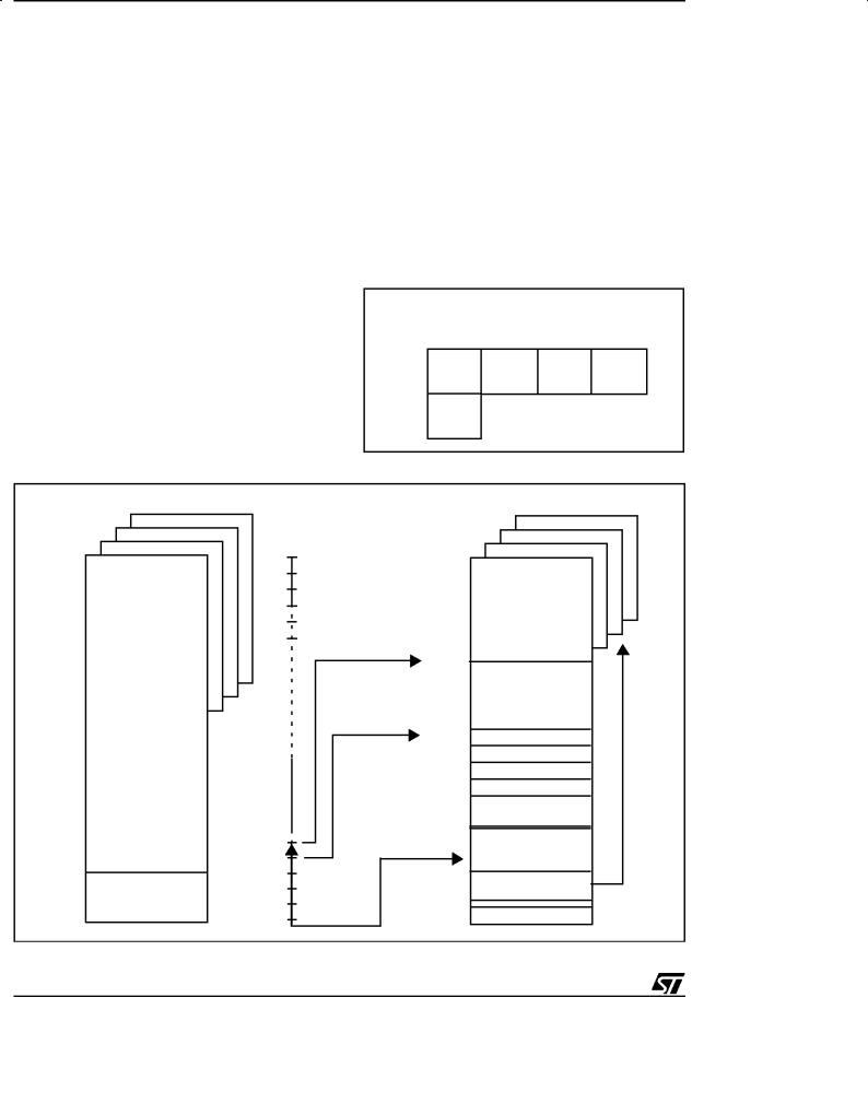
Figure 4. Memory Addressing Diagram
common (STATIC) 2K page is available all the time for interrupt vectors and common subroutines, independently of the PRPR register content.
This ªSTATICº page is directly addressed in the 0800h-0FFFh by the MSB of the Program Counter register PC 11. Note this page can also be addressed in the 000-7FFh range. It is two different ways of addressing the same physical memory.
Jump from a dynamic page to another dynamic page is achieved by jumping back to the static page, changing contents of PRPR and then jumping to the new dynamic page.
Figure 3. 8Kbytes Program Space Addressing
|
|
ROM SPACE |
|
PC |
|
|
|
SPACE |
0000h |
|
1FFFh |
000h |
|
Page 1 |
|
|
Page 0 |
Page 2 Page 3 |
|
|
Static |
||
7FFh |
|
|
|
|
Page |
|
|
800h |
Page 1 |
|
|
FFFh |
Static |
|
|
Page |
|
|
|
PROGRAM SPACE |
|
DATA SPACE |
|
|
|
0000h |
000h |
|
|
|
|
|
|
RAM / EEPROM |
|
|
BANKING AREA |
0-63 |
03Fh |
|
|
040h |
|
|
|
DATA READ-ONLY |
PROGRAM |
|
MEMORY WINDOW |
MEMORY |
07Fh |
|
|
080h |
X REGISTER |
|
081h |
Y REGISTER |
|
082h |
V REGISTER |
|
083h |
W REGISTER |
|
084h |
RAM |
|
|
|
|
0C0h |
DATA READ-ONLY |
0FF0h |
|
MEMORY |
|
WINDOW SELECT |
|
INTERRUPT & |
|
DATA RAM |
|
BANK SELECT |
|
RESET VECTORS |
|
|
|
ACCUMULATOR |
|
0FFFh |
0FFh |
VR01568
8/86
ST62T30B ST62E30B
MEMORY MAP (Cont'd)
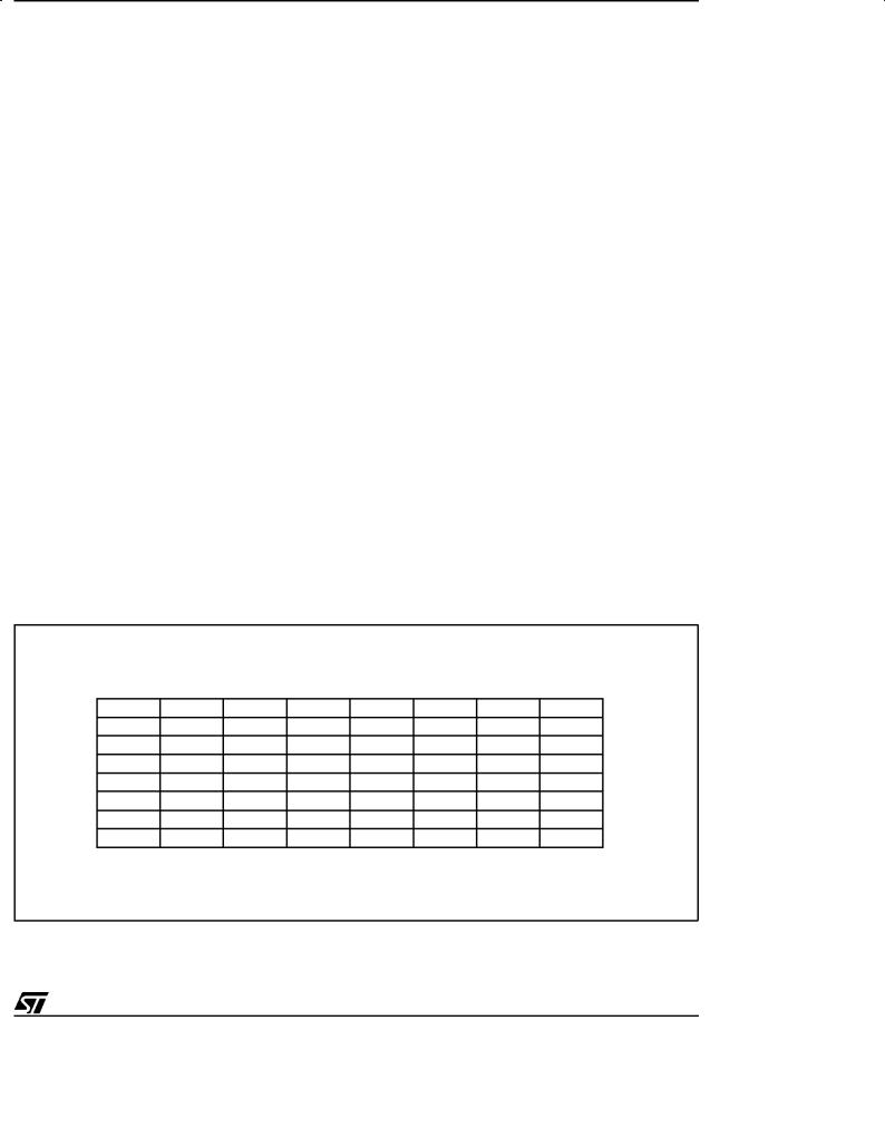
Table 1. ST62E30B/T30B Program Memory Map
ROM Page |
Device Address |
Description |
|
Page 0 |
0000h-007Fh |
Reserved |
|
0080h-07FFh |
User ROM |
||
|
|||
|
0800h-0F9Fh |
User ROM |
|
|
0FA0h-0FEFh |
Reserved |
|
Page 1 |
0FF0h-0FF7h |
Interrupt Vectors |
|
ªSTATICº |
0FF8h-0FFBh |
Reserved |
|
|
0FFCh-0FFDh |
NMI Vector |
|
|
0FFEh-0FFFh |
Reset Vector |
|
Page 2 |
0000h-000Fh |
Reserved |
|
0010h-07FFh |
User ROM |
||
|
|||
Page 3 |
0000h-000Fh |
Reserved |
|
0010h-07FFh |
User ROM |
||
|
Note: OTP/EPROM devices can be programmed with the development tools available from STMicroelectronics (ST62E3X-EPB or ST623X-KIT).
1.3.2.1 Program ROM Page Register (PRPR)
The PRPR register can be addressed like a RAM location in the Data Space at the address CAh; nevertheless it is a write only register that cannot be accessed with single-bit operations. This register is used to select the 2-Kbyte ROM bank of the Program Space that will be addressed. The number of the page has to be loaded in the PRPR register. Refer to the Program Space description for additional information concerning the use of this register. The PRPR register is not modified when an interrupt or a subroutine occurs.
Care is required when handling the PRPR register as it is write only. For this reason, it is not allowed to change the PRPR contents while executing interrupt service routine, as the service routine cannot save and then restore its previous content. This operation may be necessary if common routines and interrupt service routines take more than 2K bytes; in this case it could be necessary to divide the interrupt service routine into a (minor) part in the static page (start and end) and to a second (major) part in one of the dynamic pages. If it is impossible to avoid the writing of this register in interrupt service routines, an image of this register must be saved in a RAM location, and each time the program writes to the PRPR it must write also to the image register. The image register must be written before PRPR, so if an interrupt occurs between the two instructions the PRPR is not affected.
Program ROM Page Register (PRPR)
Address: CAh Ð Write Only
7 |
|
|
|
|
0 |
- |
- |
- |
- |
- |
- PRPR0 PRPR1 |
Bits 2-7= Not used.
Bit 5-0 = PRPR1-PRPR0: Program ROM Select.
These two bits select the corresponding page to be addressed in the lower part of the 4K program address space as specified inTable 2.
This register is undefined on Reset. Neither read nor single bit instructions may be used to address this register.
Table 2. 8Kbytes Program ROM Page Register
Coding
PRPR1 |
PRPR0 |
PC bit 11 |
Memory Page |
X |
X |
1 |
Static Page (Page 1) |
0 |
0 |
0 |
Page 0 |
0 |
1 |
0 |
Page 1 (Static Page |
1 |
0 |
0 |
Page 2 |
1 |
1 |
0 |
Page 3 |
1.3.2.2 Program Memory Protection
The Program Memory in OTP or EPROM devices can be protected against external readout of memory by selecting the READOUT PROTECTION option in the option byte.
In the EPROM parts, READOUT PROTECTION option can be disactivated only by U.V. erasure that also results into the whole EPROM context erasure.
Note: Once the Readout Protection is activated, it is no longer possible, even for STMicroelectronics, to gain access to the Program memory contents. Returned parts with a protection set can therefore not be accepted.
9/86

ST62T30B ST62E30B
MEMORY MAP (Cont'd)
1.3.3 Data Space
Data Space accommodates all the data necessary for processing the user program. This space comprises the RAM resource, the processor core and peripheral registers, as well as read-only data such as constants and look-up tables in Program memory.
1.3.3.1 Data ROM
All read-only data is physically stored in program memory, which also accommodates the Program Space. The program memory consequently contains the program code to be executed, as well as the constants and look-up tables required by the application.
The Data Space locations in which the different constants and look-up tables are addressed by the processor core may be thought of as a 64-byte window through which it is possible to access the read-only data stored in Program memory.
1.3.3.2 Data RAM/EEPROM
In ST6230B and ST62E30B devices, the data space includes 60 bytes of RAM, the accumulator (A), the indirect registers (X), (Y), the short direct registers (V), (W), the I/O port registers, the peripheral data and control registers, the interrupt option register and the Data ROM Window register (DRW register).
Additional RAM and EEPROM pages can also be addressed using banks of 64 bytes located between addresses 00h and 3Fh.
1.3.4 Stack Space
Stack space consists of six 12-bit registers which are used to stack subroutine and interrupt return addresses, as well as the current program counter contents.
Table 3. Additional RAM/EEPROM Banks.
Device |
RAM |
EEPROM |
ST62T30B/E30B |
2 x 64 bytes |
2 x 64 bytes |
Table 4. ST62T30B/E30B Data Memory Space
DATA and EEPROM |
000h |
|
03Fh |
||
|
||
DATA ROM WINDOW AREA |
040h |
|
07Fh |
||
|
||
X REGISTER |
080h |
|
Y REGISTER |
081h |
|
V REGISTER |
082h |
|
W REGISTE R |
083h |
|
DATA RAM |
084h |
|
0BFh |
||
|
||
PORT A DATA REGISTER |
0C0h |
|
PORT B DATA REGISTER |
0C1h |
|
PORT C DATA REGISTER |
0C2h |
|
PORT D DATA REGISTER |
0C3h |
|
PORT A DIRECTION REGISTER |
0C4h |
|
PORT B DIRECTION REGISTER |
0C5h |
|
PORT C DIRECTION REGISTER |
0C6h |
|
PORT D DIRECTION REGISTER |
0C7h |
|
INTERRUPT OPTION REGISTER |
0C8h* |
|
DATA ROM WINDOW REGISTER |
0C9h* |
|
ROM BANK SELECT REGISTER |
0CAh* |
|
RAM/EEPROM BANK SELECT REGISTER |
0CBh* |
|
PORT A OPTION REGISTER |
0CCh |
|
PORT B OPTION REGISTER |
0CDh |
|
PORT C OPTION REGISTE R |
0CEh |
|
PORT D OPTION REGISTE R |
0CFh |
|
A/D DATA REGISTE R |
0D0h |
|
A/D CONTROL REGISTER |
0D1h |
|
TIMER 1 PRESCALER REGISTER |
0D2h |
|
TIMER 1 COUNTER REGISTER |
0D3h |
|
TIMER 1 STATUS/CONTROL REGISTER |
0D4h |
|
RESERVED |
0D5h |
|
UART DATA SHIFT REGISTER |
0D6h |
|
UART STATUS CONTROL REGISTER |
0D7h |
|
WATCHDOG REGISTER |
0D8h |
|
RESERVED |
0D9h |
|
I/O INTERRUPT POLARITY REGISTER |
0DAh |
|
OSCILLATOR CONTROL REGISTER |
0DBh |
|
SPI INTERRUPT DISABLE REGISTER |
0DCh* |
|
SPI DATA REGISTER |
0DDh |
|
RESERVED |
0DEh |
|
EEPROM CONTROL REGISTER |
0DFh |
|
ARTIM16 COMPARE MASK REG. LOW BYTE MASK |
0E0h |
|
ARTIM16 2ND STATUS CONTROL REGISTE R SCR2 |
0E1h |
|
ARTIM16 3RD STATUS CONTROL REGISTE R SCR3 |
0E2h |
|
ARTIM16 4TH STATUS CONTROL REGISTER SCR4 |
0E3h |
|
ARTIM16 1ST STATUS CONTROL REGISTER SCR1 |
0E8h |
|
ARTIM16 RELOAD CAPTURE REG. HIGH BYTE RLCP |
0E9h |
|
ARTIM16 RELOAD CAPTURE REG. LOW BYTE RLCP |
0EAh |
|
ARTIM16 CAPTURE REGISTER HIGH BYTE CP |
0EBh |
|
ARTIM16 CAPTURE REGISTER LOW BYTE CP |
0ECh |
|
ARTIM16 COMPAREVALUE REGISTER HIGH BYTECMP |
0EDh |
|
ARTIM 16 COMPARE VALUE REGISTER LOWBYTE CMP |
0EEh |
|
ARTIM 16 COMPARE MASK REG. HIGH BYTE MASK |
0EFh |
|
RESERVED |
0F0h |
|
|
0FBh |
|
|
OFCh |
|
RESERVED |
0FDh |
|
|
0FEh |
|
ACCUMULATOR |
OFFh |
|
* WRITE ONLY REGISTER |
|
10/86
ST62T30B ST62E30B
MEMORY MAP (Cont'd)
1.3.5 Data Window Register (DWR)
The Data read-only memory window is located from address 0040h to address 007Fh in Data space. It allows direct reading of 64 consecutive bytes located anywhere in program memory, between address 0000h and 1FFFh (top memory address depends on the specific device). All the program memory can therefore be used to store either instructions or read-only data. Indeed, the window can be moved in steps of 64 bytes along the program memory by writing the appropriate code in the Data Window Register (DWR).
The DWR can be addressed like any RAM location in the Data Space, it is however a write-only register and therefore cannot be accessed using singlebit operations. This register is used to position the 64-byte read-only data window (from address 40h to address 7Fh of the Data space) in program memory in 64-byte steps. The effective address of the byte to be read as data in program memory is obtained by concatenating the 6 least significant bits of the register address given in the instruction (as least significant bits) and the content of the DWR register (as most significant bits), as illustrated in Figure 5 below. For instance, when addressing location 0040h of the Data Space, with 0 loaded in the DWR register, the physical location addressed in program memory is 00h. The DWR register is not cleared on reset, therefore it must be written to prior to the first access to the Data readonly memory window area.
Data Window Register (DWR)
Address: 0C9h Ð Write Only
7 |
0 |
-DWR6 DWR5 DWR4 DWR3 DWR2 DWR1 DWR0
Bits 7 = Not used.
Bit 6-0 = DWR5-DWR0: Data read-only memory Window Register Bits. These are the Data readonly memory Window bits that correspond to the upper bits of the data read-only memory space.
Caution: This register is undefined on reset. Neither read nor single bit instructions may be used to address this register.
Note: Care is required when handling the DWR register as it is write only. For this reason, the DWR contents should not be changed while executing an interrupt service routine, as the service routine cannot save and then restore the register's previous contents. If it is impossible to avoid writing to the DWR during the interrupt service routine, an image of the register must be saved in a RAM location, and each time the program writes to the DWR, it must also write to the image register. The image register must be written first so that, if an interrupt occurs between the two instructions, the DWR is not affected.
Figure 5. Data read-only memory Window Memory Addressing
DATA ROM |
13 |
12 |
11 |
10 |
9 |
8 |
7 |
6 |
5 |
4 |
3 |
2 |
1 |
0 |
PROGRAM SPACE ADDRESS |
|
|
|
|
|
|
|
|
|
|
|
|
|
|
READ |
|
WINDOW REGISTER 7 |
6 |
5 |
4 |
3 |
2 |
1 |
0 |
|
|
|
|
|
|
||
|
|
|
|
|
|
|
|||||||||
CONTENTS |
|
|
|
|
|
|
|
|
5 |
4 |
3 |
2 |
1 |
0 |
DATA SPACE ADDRESS |
(DWR) |
|
|
|
|
|
|
|
|
|||||||
|
|
|
|
|
|
0 |
1 |
|
|
|
|
|
|
40h-7Fh |
|
|
|
|
|
|
|
|
|
|
|
|
|
|
|||
|
|
|
|
|
|
|
|
|
|
|
|
|
|
|
IN INSTRUCTION |
Example:
DWR=28h |
0 |
1 |
0 |
1 |
0 |
0 |
0 |
|
|
|
|
|
|
|
|
|
|
|
|
|
0 |
1 |
0 |
1 |
1 |
0 |
0 |
1 |
DATA SPACE ADDRESS |
|
|
|
|
|
|
59h |
||||||||
|
|
|
|
|
|
|
|
|
|
|
|
|
|
|
ROM |
0 |
1 |
0 |
1 |
0 |
0 |
0 |
0 |
1 |
1 |
0 |
0 |
1 |
|
ADDRESS:A19h |
|
|||||||||||||
|
|
|
|
|
|
|
|
|
|
|
|
|
|
VR0A1573
11/86

ST62T30B ST62E30B
MEMORY MAP (Cont'd)
1.3.6 Data RAM/EEPROM Bank Register (DRBR)
Address: CBh Ð Write only
7 |
|
0 |
- |
- |
- DRBR4 DRBR3 - DRBR1 DRBR0 |
Bit 7-5 = These bits are not used
Bit 4 - DRBR4. This bit, when set, selects RAM Page 2.
Bit 3 - DRBR3. This bit, when set, selects RAM Page 1.
Bit2. This bit is not used.
Bit 1 - DRBR1. This bit, when set, selects EEPROM Page 1.
Bit 0 - DRBR0. This bit, when set, selects EEPROM Page 0.
The selection of the bank is made by programming the Data RAM Bank Switch register (DRBR register) located at address CBh of the Data Space according to Table 1. No more than one bank should be set at a time.
The DRBR register can be addressed like a RAM Data Space at the address CBh; nevertheless it is a write only register that cannot be accessed with single-bit operations. This register is used to select the desired 64-byte RAM/EEPROM bank of the Data Space. The number of banks has to be loaded in the DRBR register and the instruction has to point to the selected location as if it was in bank 0 (from 00h address to 3Fh address).
This register is not cleared during the MCU initialization, therefore it must be written before the first access to the Data Space bank region. Refer to the Data Space description for additional information. The DRBR register is not modified when an interrupt or a subroutine occurs.
Notes:
Care is required when handling the DRBR register as it is write only. For this reason, it is not allowed to change the DRBR contents while executing interrupt service routine, as the service routine cannot save and then restore its previous content. If it is impossible to avoid the writing of this register in interrupt service routine, an image of this register must be saved in a RAM location, and each time the program writes to DRBR it must write also to the image register. The image register must be written first, so if an interrupt occurs between the two instructions the DRBR is not affected.
In DRBR Register, only 1 bit must be set. Otherwise two or more pages are enabled in parallel, producing errors.
Table 5. Data RAM Bank Register Set-up
DRBR |
ST62T30B/E30B |
00 |
None |
01 |
EEPROM Page 0 |
02 |
EEPROM Page 1 |
08 |
RAM Page 1 |
10h |
RAM Page 2 |
other |
Reserved |
12/86
ST62T30B ST62E30B
MEMORY MAP (Cont'd)
1.3.7 EEPROM Description
EEPROM memory is located in 64-byte pages in data space. This memory may be used by the user program for non-volatile data storage.
Data space from 00h to 3Fh is paged as described in Table 6. EEPROM locations are accessed directly by addressing these paged sections of data space.
The EEPROM does not require dedicated instructions for read or write access. Once selected via the Data RAM Bank Register, the active EEPROM page is controlled by the EEPROM Control Register (EECTL), which is described below.
Bit E20FF of the EECTL register must be reset prior to any write or read access to the EEPROM. If no bank has been selected, or if E2OFF is set, any access is meaningless.
Programming must be enabled by setting the E2ENA bit of the EECTL register.
The E2BUSY bit of the EECTL register is set when the EEPROM is performing a programming cycle. Any access to the EEPROM when E2BUSY is set is meaningless.
Provided E2OFF and E2BUSY are reset, an EEPROM location is read just like any other data location, also in terms of access time.
Writing to the EEPROM may be carried out in two modes: Byte Mode (BMODE) and Parallel Mode
(PMODE). In BMODE, one byte is accessed at a time, while in PMODE up to 8 bytes in the same row are programmed simultaneously (with consequent speed and power consumption advantages, the latter being particularly important in battery powered circuits).
General Notes:
Data should be written directly to the intended address in EEPROM space. There is no buffer memory between data RAM and the EEPROM space.
When the EEPROM is busy (E2BUSY = ª1º) EECTL cannot be accessed in write mode, it is only possible to read the status of E2BUSY. This implies that as long as the EEPROM is busy, it is not possible to change the status of the EEPROM Control Register. EECTL bits 4 and 5 are reserved and must never be set.
Care is required when dealing with the EECTL register, as some bits are write only. For this reason, the EECTL contents must not be altered while executing an interrupt service routine.
If it is impossible to avoid writing to this register within an interrupt service routine, an image of the register must be saved in a RAM location, and each time the program writes to EECTL it must also write to the image register. The image register must be written to first so that, if an interrupt occurs between the two instructions, the EECTL will not be affected.
Table 6. Row Arrangement for Parallel Writing of EEPROM Locations
|
|
|
|
|
|
|
|
Dataspace |
|
|
|
|
|
|
|
|
addresses. |
|
|
|
|
|
|
|
|
Banks 0 and 1. |
Byte |
0 |
1 |
2 |
3 |
4 |
5 |
6 |
7 |
ROW7 |
|
|
|
|
|
|
|
38h-3Fh |
ROW6 |
|
|
|
|
|
|
|
30h-37h |
ROW5 |
|
|
|
|
|
|
|
28h-2Fh |
ROW4 |
|
|
|
|
|
|
|
20h-27h |
ROW3 |
|
|
|
|
|
|
|
18h-1Fh |
ROW2 |
|
|
|
|
|
|
|
10h-17h |
ROW1 |
|
|
|
|
|
|
|
08h-0Fh |
ROW0 |
|
|
|
|
|
|
|
00h-07h |
Up to 8 bytes in each row may be programmed simultaneously in Parallel Write mode.
The number of available 64-byte banks (1 or 2) is device dependent.
13/86

ST62T30B ST62E30B
MEMORY MAP (Cont'd)
Additional Notes on Parallel Mode:
If the user wishes to perform parallel programming, the first step should be to set the E2PAR2 bit. From this time on, the EEPROM will be addressed in write mode, the ROW address will be latched and it will be possible to change it only at the end of the programming cycle, or by resetting E2PAR2 without programming the EEPROM. After the ROW address is latched, the MCU can only ªseeº the selected EEPROM row and any attempt to write or read other rows will produce errors.
The EEPROM should not be read while E2PAR2 is set.
As soon as the E2PAR2 bit is set, the 8 volatile ROW latches are cleared. From this moment on, the user can load data in all or in part of the ROW. Setting E2PAR1 will modify the EEPROM registers corresponding to the ROW latches accessed after E2PAR2. For example, if the software sets E2PAR2 and accesses the EEPROM by writing to addresses 18h, 1Ah and 1Bh, and then sets E2PAR1, these three registers will be modified simultaneously; the remaining bytes in the row will be unaffected.
Note that E2PAR2 is internally reset at the end of the programming cycle. This implies that the user must set the E2PAR2 bit between two parallel programming cycles. Note that if the user tries to set E2PAR1 while E2PAR2 is not set, there will be no programming cycle and the E2PAR1 bit will be unaffected. Consequently, the E2PAR1 bit cannot be set if E2ENA is low. The E2PAR1 bit can be set by the user, only if the E2ENA and E2PAR2 bits are also set.
EEPROM Control Register (EECTL)
Address: DFh Ð Read/Write
Reset status: 00h
7 |
0 |
D7 E2OFF D5 D4 E2PAR1 E2PAR2 E2BUSY E2ENA
Bit 7 = D7: Unused.
Bit 6 = E2OFF: Stand-by Enable Bit.WRITE ONLY. If this bit is set the EEPROM is disabled (any access will be meaningless) and the power consumption of the EEPROM is reduced to its lowest value.
Bit 5-4 = D5-D4: Reserved. MUST be kept reset.
Bit 3 = E2PAR1: Parallel Start Bit. WRITE ONLY. Once in Parallel Mode, as soon as the user software sets the E2PAR1 bit, parallel writing of the 8 adjacent registers will start. This bit is internally reset at the end of the programming procedure. Note that less than 8 bytes can be written if required, the undefined bytes being unaffected by the parallel programming cycle; this is explained in greater detail in the Additional Notes on Parallel Mode overleaf.
Bit 2 = E2PAR2: Parallel Mode En. Bit. WRITE ONLY. This bit must be set by the user program in order to perform parallel programming. If E2PAR2 is set and the parallel start bit (E2PAR1) is reset, up to 8 adjacent bytes can be written simultaneously. These 8 adjacent bytes are considered as a row, whose address lines A7, A6, A5, A4, A3 are fixed while A2, A1 and A0 are the changing bits, as illustrated in Table 6. E2PAR2 is automatically reset at the end of any parallel programming procedure. It can be reset by the user software before starting the programming procedure, thus leaving the EEPROM registers unchanged.
Bit 1 = E2BUSY: EEPROM Busy Bit. READ ONLY. This bit is automatically set by the EEPROM control logic when the EEPROM is in programming mode. The user program should test it before any EEPROM read or write operation; any attempt to access the EEPROM while the busy bit is set will be aborted and the writing procedure in progress will be completed.
Bit 0 = E2ENA: EEPROM Enable Bit. WRITE ONLY. This bit enables programming of the EEPROM cells. It must be set before any write to the EEPROM register. Any attempt to write to the EEPROM when E2ENA is low is meaningless and will not trigger a write cycle.
14/86

ST62T30B ST62E30B
1.4 PROGRAMMING MODES
1.4.1 Option Byte
The Option Byte allows configuration capability to the MCUs. Option byte's content is automatically read, and the selected options enabled, when the chip reset is activated.
It can only be accessed during the programming mode. This access is made either automatically (copy from a master device) or by selecting the OPTION BYTE PROGRAMMING mode of the programmer.
The option byte is located in a non-user map. No address has to be specified.
EPROM Code Option Byte
7 |
0 |
-PORTPULL EXTCNTL PROTECT PULLTIM PULLNMI WDACT OSGEN
Bit 7. Reserved.
Bit 6 = PORT PULL. This bit must be set high to have pull-up input state at reset on the I/O port. When this bit is low, I/O ports are in input without pull-up (high impedance) state at reset
Bit 5 = EXTCNTL. This bit selects the External STOP Mode capability. When EXTCNTL is high, pin NMI controls if the STOP mode can be accessed when the watchdog is active. When EXTCNTL is low, the STOP instruction is processed as a WAIT as soon as the watchdog is active.
Bit 4 = PROTECT. This bit allows the protection of the software contents against piracy. When the bit PROTECT is set high, readout of the OTP contents is prevented by hardware. No programming equipment is able to gain access to the user program. When this bit is low, the user program can be read.
Bit 3 = TIM PULL. This bit must be set high to configure the TIMER pin with a pull up resistor. When it is low, no pull up is provided.
Bit 2 = NMI PULL. This bit must be set high to configure the NMI pin with a pull up resistor when it is low, no pull up is provided.
Bit 1 = WDACT. This bit controls the watchdog activation. When it is high, hardware activation is selected. The software activation is selected when WDACT is low.
Bit 0 = OSGEN. This bit must be set high to enable the oscillator Safe Guard. When this bit is low, the OSG is disabled.
The Option byte is written during programming either by using the PC menu (PC driven Mode) or automatically (stand-alone mode)
1.4.2 Program Memory
EPROM/OTP programming mode is set by a
+12.5V voltage applied to the TEST/V pin. The
PP
programming flow of the ST62T30B/E30B is described in the User Manual of the EPROM Programming Board.
The MCUs can be programmed with the ST62E3xB EPROM programming tools available from STMicroelectronics.
1.4.3 EEPROM Data Memory
EEPROM data pages are supplied in the virgin state FFh. Partial or total programming of EEPROM data memory can be performed either through the application software, or through an external programmer. Any STMicroelectronics tool used for the program memory (OTP/EPROM) can also be used to program the EEPROM data memory.
1.4.4 EPROM Erasing
The EPROM of the windowed package of the MCUs may be erased by exposure to Ultra Violet light. The erasure characteristic of the MCUs is such that erasure begins when the memory is exposed to light with a wave lengths shorter than approximately 4000Å. It should be noted that sunlights and some types of fluorescent lamps have wavelengths in the range 3000-4000Å.
It is thus recommended that the window of the MCUs packages be covered by an opaque label to prevent unintentional erasure problems when testing the application in such an environment.
The recommended erasure procedure of the MCUs EPROM is the exposure to short wave ultraviolet light which have a wave-length 2537A. The integrated dose (i.e. U.V. intensity x exposure time) for erasure should be a minimum of 15Wsec/cm2. The erasure time with this dosage is approximately 15 to 20 minutes using an ultraviolet lamp with 12000μW/cm2 power rating. The ST62E30B should be placed within 2.5cm (1Inch) of the lamp tubes during erasure.
15/86
ST62T30B ST62E30B
2 CENTRAL PROCESSING UNIT
2.1 INTRODUCTION
The CPU Core of ST6 devices is independent of the I/O or Memory configuration. As such, it may be thought of as an independent central processor communicating with on-chip I/O, Memory and Peripherals via internal address, data, and control buses. In-core communication is arranged as shown in Figure 6; the controller being externally linked to both the Reset and Oscillator circuits, while the core is linked to the dedicated on-chip peripherals via the serial data bus and indirectly, for interrupt purposes, through the control registers.
2.2 CPU REGISTERS
The ST6 Family CPU core features six registers and three pairs of flags available to the programmer. These are described in the following paragraphs.
Accumulator (A). The accumulator is an 8-bit general purpose register used in all arithmetic calculations, logical operations, and data manipulations. The accumulator can be addressed in Data space as a RAM location at address FFh. Thus the ST6 can manipulate the accumulator just like any other register in Data space.
Figure 6. ST6 Core Block Diagram
Indirect Registers (X, Y). These two indirect registers are used as pointers to memory locations in Data space. They are used in the register-indirect addressing mode. These registers can be addressed in the data space as RAM locations at addresses 80h (X) and 81h (Y). They can also be accessed with the direct, short direct, or bit direct addressing modes. Accordingly, the ST6 instruction set can use the indirect registers as any other register of the data space.
Short Direct Registers (V, W). These two registers are used to save a byte in short direct addressing mode. They can be addressed in Data space as RAM locations at addresses 82h (V) and 83h (W). They can also be accessed using the direct and bit direct addressing modes. Thus, the ST6 instruction set can use the short direct registers as any other register of the data space.
Program Counter (PC). The program counter is a 12-bit register which contains the address of the next ROM location to be processed by the core. This ROM location may be an opcode, an operand, or the address of an operand. The 12-bit length allows the direct addressing of 4096 bytes in Program space.
|
|
0,01 TO 8MHz |
|
|
|
|
RESET |
OSCin |
OSCout |
|
|
|
|
|
|
||
|
|
|
INTERR UPTS |
||
|
|
CONTROLLER |
|
|
|
|
|
|
|
|
DATA SPACE |
|
|
FLAG |
CONTROL |
|
|
|
OPCODE |
SIGNALS |
|
DATA |
|
|
VALUES |
ADDRESS /READ LINE |
|
||
|
|
|
|||
|
|
2 |
|
|
RAM/EEPROM |
|
|
|
|
|
|
PROGRAM |
|
|
|
|
DATA |
ROM/EPROM |
|
|
ADDRESS |
|
|
|
|
256 |
ROM/EPROM |
||
|
|
|
DECODER |
|
|
|
|
|
|
|
|
|
|
A-DATA B-DATA |
|
DEDICATIONS |
|
|
|
|
|
|
|
|
|
|
|
|
ACCUMULATOR |
12 |
Program Counter |
|
|
|
|
and |
FLAGS |
|
|
|
|
|
6 LAYER STACK |
ALU |
|
|
|
RESULTS TO DATA SPACE (WRITE LINE)
VR01811
16/86
CPU REGISTERS (Cont'd)
However, if the program space contains more than 4096 bytes, the additional memory in program space can be addressed by using the Program Bank Switch register.
The PC value is incremented after reading the address of the current instruction. To execute relative jumps, the PC and the offset are shifted through the ALU, where they are added; the result is then shifted back into the PC. The program counter can be changed in the following ways:
-JP (Jump) instructionPC=Jump address
-CALL instructionPC= Call address
-Relative Branch Instruction.PC= PC +/- offset
- Interrupt |
PC=Interrupt vector |
- Reset |
PC= Reset vector |
-RET & RETI instructionsPC= Pop (stack)
-Normal instructionPC= PC + 1
Flags (C, Z). The ST6 CPU includes three pairs of flags (Carry and Zero), each pair being associated with one of the three normal modes of operation: Normal mode, Interrupt mode and Non Maskable Interrupt mode. Each pair consists of a CARRY flag and a ZERO flag. One pair (CN, ZN) is used during Normal operation, another pair is used during Interrupt mode (CI, ZI), and a third pair is used in the Non Maskable Interrupt mode (CNMI, ZNMI).
The ST6 CPU uses the pair of flags associated with the current mode: as soon as an interrupt (or a Non Maskable Interrupt) is generated, the ST6 CPU uses the Interrupt flags (resp. the NMI flags) instead of the Normal flags. When the RETI instruction is executed, the previously used set of flags is restored. It should be noted that each flag set can only be addressed in its own context (Non Maskable Interrupt, Normal Interrupt or Main routine). The flags are not cleared during context switching and thus retain their status.
The Carry flag is set when a carry or a borrow occurs during arithmetic operations; otherwise it is cleared. The Carry flag is also set to the value of the bit tested in a bit test instruction; it also participates in the rotate left instruction.
The Zero flag is set if the result of the last arithmetic or logical operation was equal to zero; otherwise it is cleared.
Switching between the three sets of flags is performed automatically when an NMI, an interrupt or a RETI instructions occurs. As the NMI mode is
ST62T30B ST62E30B
automatically selected after the reset of the MCU, the ST6 core uses at first the NMI flags.
Stack. The ST6 CPU includes a true LIFO hardware stack which eliminates the need for a stack pointer. The stack consists of six separate 12-bit RAM locations that do not belong to the data space RAM area. When a subroutine call (or interrupt request) occurs, the contents of each level are shifted into the next higher level, while the content of the PC is shifted into the first level (the original contents of the sixth stack level are lost). When a subroutine or interrupt return occurs (RET or RETI instructions), the first level register is shifted back into the PC and the value of each level is popped back into the previous level. Since the accumulator, in common with all other data space registers, is not stored in this stack, management of these registers should be performed within the subroutine. The stack will remain in its ªdeepestº position if more than 6 nested calls or interrupts are executed, and consequently the last return address will be lost. It will also remain in its highest position if the stack is empty and a RET or RETI is executed. In this case the next instruction will be executed.
Figurel 7. ST6 CPU Programming Mode
INDEX |
b 7 |
X RE G. POINTER |
b0 |
SHORT |
||
|
|
|
|
|||
REGISTER |
|
|
|
|
||
b 7 |
Y REG. POINTER |
b0 |
DIRECT |
|||
|
||||||
|
ADDRESSING |
|||||
|
|
|
|
|
||
|
b 7 |
V REGISTER |
b0 |
MODE |
||
|
|
|||||
|
b 7 |
W REGISTER |
|
b0 |
|
|
|
b 7 ACCUMULATOR |
b0 |
|
|||
b11 |
PROGRAM COUNTER |
|
b0 |
|
||
|
SIX LEVELS |
|
|
|
||
|
STACK REGISTER |
|
|
|
||
NORMAL FLAGS |
|
C |
Z |
|
||
INTERRUPT FLAGS |
C |
Z |
|
|||
NMI FLAGS |
|
C |
Z |
|
||
|
|
|
|
|
VA000423 |
|
17/86
ST62T30B ST62E30B
3 CLOCKS, RESET, INTERRUPTS AND POWER SAVING MODES
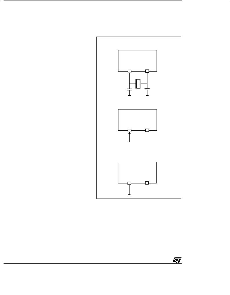
3.1 CLOCK SYSTEM
The MCU features a Main Oscillator which can be driven by an external clock, or used in conjunction with an AT-cut parallel resonant crystal or a suitable ceramic resonator. In addition, a Low Frequency Auxiliary Oscillator (LFAO) can be switched in for security reasons, to reduce power consumption, or to offer the benefits of a back-up clock system.
The Oscillator Safeguard (OSG) option filters spikes from the oscillator lines, provides access to the LFAO to provide a backup oscillator in the event of main oscillator failure and also automati-
cally limits the internal clock frequency (f ) as a
INT
function of VDD, in order to guarantee correct operation. These functions are illustrated inFigure 9, Figure 10, Figure 11 and Figure 12.
Figure 8 illustrates various possible oscillator configurations using an external crystal or ceramic resonator, an external clock input or the lowest cost solution using only the LFAO. CL1 an CL2 should have a capacitance intherange 12 to22 pFforanoscillator frequency in the 4-8 MHz range.
The internal MCU clock frequency (f ) is divided
INT
by 12 to drive the Timer and the Watchdog timer, and by 13 to drive the CPU core, while the A/D converter is driven by fINT divided either by 6 or by 12 as may be seen inFigure 11.
With an 8MHz oscillator frequency, the fastest machine cycle is therefore 1.625μs.
A machine cycle is the smallest unit of time needed to execute any operation (for instance, to increment the Program Counter). An instruction may require two, four, or five machine cycles for execution.
3.1.1 Main Oscillator
The main oscillator can be turned off (when the OSG ENABLED option is selected) by setting the OSCOFF bit of the OSCR Control Register. The Low Frequency Auxiliary Oscillator is automatically started.
Figure 8. Oscillator Configurations
CRYSTAL/R ESONATOR CLOCK
ST6xxx
OSCin OSCout
CL1n |
CL2 |
VA0016
EXTERNAL CLOCK
ST6xxx
OSCin OSCout
NC
VA0015A
INTEGRATE D CLOCK
OSG ENABLED option
ST6xxx
OSCin OSCout
NC
18/86

ST62T30B ST62E30B
CLOCK SYSTEM (Cont'd)
Turning on the main oscillator is achieved by resetting the OSCOFF bit of the OSCR Register or by resetting the MCU. Restarting the main oscillator implies a delay comprising the oscillator start up delay period plus the duration of the software instruction at fLFAO clock frequency.
3.1.2Low Frequency Auxiliary Oscillator (LFAO)
The Low Frequency Auxiliary Oscillator has three main purposes. Firstly, it can be used to reduce power consumption in non timing critical routines. Secondly, it offers a fully integrated system clock, without any external components. Lastly, it acts as a safety oscillator in case of main oscillator failure.
This oscillator is available when the OSG ENABLED option is selected. In this case, it automatically starts one of its periods after the first missing edge from the main oscillator, whatever the reason (main oscillator defective, no clock circuitry provided, main oscillator switched off...).
User code, normal interrupts, WAIT and STOP instructions, are processed as normal, at the reduced fLFAO frequency. The A/D converter accuracy is decreased, since the internal frequency is below 1MHz.
At power on, the Low Frequency Auxiliary Oscillator starts faster than the Main Oscillator. It therefore feeds the on-chip counter generating the POR delay until the Main Oscillator runs.
The Low Frequency Auxiliary Oscillator is automatically switched off as soon as the main oscillator starts.
OSCR
Address: 0DBh Ð Read/Write
7 |
|
|
|
|
|
|
0 |
|
- |
- |
- |
- |
- |
- |
- |
OSC |
|
OFF |
||||||||
|
|
|
|
|
|
|
Bit 7-1= These bits are not used and must be kept cleared after reset.
Bit 0 = OSCOFF. Main oscillator turn-off. When low, this bit enables main oscillator to run. The main oscillator is switched off when OSCOFF is high.
3.1.3 Oscillator Safe Guard
The Oscillator Safe Guard (OSG) affords drastically increased operational integrity in ST62xx devices. The OSG circuit provides three basic functions: it filters spikes from the oscillator lines which would result in over frequency to the ST62 CPU; it gives access to the Low Frequency Auxiliary Oscillator (LFAO), used to ensure minimum processing in case of main oscillator failure, to offer reduced power consumption or to provide a fixed frequency low cost oscillator; finally, it automatically limits the internal clock frequency as a function of supply voltage, in order to ensure correct operation even if the power supply should drop.
The OSG is enabled or disabled by choosing the relevant OSG option. It may be viewed as a filter whose cross-over frequency is device dependent.
Spikes on the oscillator lines result in an effectively increased internal clock frequency. In the absence of an OSG circuit, this may lead to an over frequency for a given power supply voltage. The OSG filters out such spikes (as illustrated inFigure 9). In all cases, when the OSG is active, the maximum internal clock frequency, fINT, is limited to fOSG, which is supply voltage dependent. This relationship is illustrated inFigure 12.
When the OSG is enabled, the Low Frequency Auxiliary Oscillator may be accessed. This oscillator starts operating after the first missing edge of the main oscillator (see Figure 10).
Over-frequency, at a given power supply level, is seen by the OSG as spikes; it therefore filters out some cycles in order that the internal clock frequency of the device is kept within the range the
particular device can stand (depending on V ),
DD
and below fOSG: the maximum authorised frequency with OSG enabled.
Note. The OSG should be used wherever possible as it provides maximum safety. Care must be taken, however, as it can increase power consumption and reduce the maximum operating frequency to fOSG.
19/86
ST62T30B ST62E30B
CLOCK SYSTEM (Cont'd)
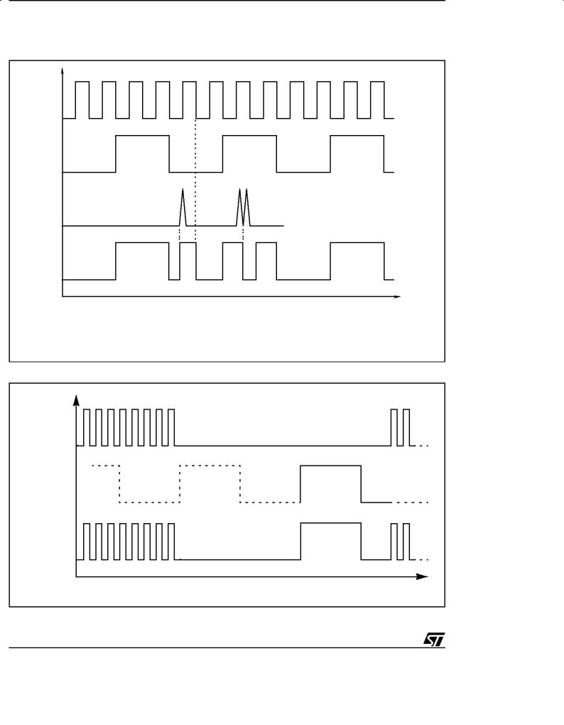
Figure 9. OSG Filtering Principle
(1)
(2)
(3)
(4)
(1)Maximum Frequency for the device to work correctly
(2)Actual Quartz Crystal Frequency at OSCin pin
(3)Noise from OSCin
(4)Resulting Internal Frequency
Figure 10. OSG Emergency Oscillator Principle
Main
Oscillator
Emergency
Oscillator
Internal
Frequency
VR001932
VR001933
20/86
ST62T30B ST62E30B
CLOCK SYSTEM (Cont'd)
Figure 11. Clock Circuit Block Diagram
|
|
|
|
|
|
|
|
|
POR |
|
|
|
|
OSG |
|
|
|
|
: 13 |
Core |
|
|
|
|
|
|
|
|
|
|
|
|
|
|
|
|
|
|
|
|
|
TIMER 1 |
|
MAIN |
|
|
|
|
M |
|
fINT |
: 12 |
Watchdog |
|
OSCILLATOR |
|
|
|
U |
|
|
|
|
||
|
|
|
X |
|
|
|
|
|
||
|
|
|
|
|
|
|
|
M |
|
|
|
|
|
|
|
|
|
|
|
ADC |
|
|
|
|
|
|
|
|
|
: 6 |
U |
|
|
|
|
|
|
|
|
|
X |
|
|
|
|
|
LFAO |
|
|
|
|
|
|
|
|
|
|
|
|
|
|
|
: 1 |
ARTIMER 16 |
|
|
|
|
|
|
|
|
|
|
||
|
|
|
|
Main Oscillator off |
|
|
|
|
|
|
Figure 12. Maximum Operating Frequency (f |
) versus Supply Voltage (V ) |
|
|
|||||||
|
|
|
|
MAX |
|
|
DD |
|
|
|
Maximum FREQUENCY (MHz) |
|
|
|
|
|
|
|
|||
8 |
|
|
|
|
|
|
|
|
|
|
7 |
|
|
|
|
|
|
|
|
|
|
6 |
NOT |
|
4 |
|
3 |
|
|
|
|
|
GUARANTEED AREATHISIN |
|
|
|
|
|
|
|
|||
|
ISFUNCTIONALITY |
|
|
|
|
|
|
|
||
|
|
|
|
|
fOSG |
|
|
|
||
|
|
|
|
|
|
|
|
|
|
|
5 |
|
|
|
|
|
|
|
|
|
|
4 |
|
|
|
|
2 |
|
fOSG Min |
|
|
|
|
|
|
|
|
|
|
|
|
|
|
3 |
|
|
|
|
|
|
|
|
|
|
2 |
|
|
|
|
|
|
|
|
|
|
|
|
|
|
|
1 |
|
|
|
|
|
1 |
2.5 |
3 |
3.5 |
4 |
4.5 |
5 |
|
5.5 |
6 |
|
|
|
|
||||||||
SUPPLY VOLTAGE (VDD)
VR01807
Notes:
1.In this area, operation is guaranteed at the quartz crystal frequency.
2.When the OSG is disabled, operation in this area is guaranteed at the crystal frequency. When the OSG
is enabled, operation in this area is guaranteed at a frequency of at least f
OSG Min.
3. When the OSG is disabled, operation in this area is guaranteed at the quartz crystal frequency. When
the OSG is enabled, access to this area is prevented. The internal frequency is kept a f
OSG.
4. When the OSG is disabled, operation in this area is not guaranteed
When the OSG is enabled, access to this area is prevented. The internal frequency is kept at f
OSG.
21/86
ST62T30B ST62E30B
3.2 RESETS
The MCU can be reset in three ways:
±by the external Reset input being pulled low;
±by Power-on Reset;
±by the digital Watchdog peripheral timing out.
3.2.1 RESET Input
The RESET pin may be connected to a device of the application board in order to reset the MCU if required. The RESET pin may be pulled low in RUN, WAIT or STOP mode. This input can be used to reset the MCU internal state and ensure a correct start-up procedure. The pin is active low and features a Schmitt trigger input. The internal Reset signal is generated by adding a delay to the external signal. Therefore even short pulses on the RESET pin are acceptable, provided VDD has completed its rising phase and that the oscillator is running correctly (normal RUN or WAIT modes). The MCU is kept in the Reset state as long as the RESET pin is held low.
If RESET activation occurs in the RUN or WAIT modes, processing of the user program is stopped (RUN mode only), the Inputs and Outputs are configured as inputs with pull-up resistors and the main Oscillator is restarted. When the level on the RESET pin then goes high, the initialization sequence is executed following expiry of the internal delay period.
If RESET pin activation occurs in the STOP mode, the oscillator starts up and all Inputs and Outputs are configured as inputs with pull-up resistors. When the level of the RESET pin then goes high, the initialization sequence is executed following expiry of the internal delay period.
3.2.2 Power-on Reset
The function of the POR circuit consists in waking up the MCU at an appropriate stage during the power-on sequence. At the beginning of this sequence, the MCU is configured in the Reset state: all I/O ports are configured as inputs with pull-up resistors and no instruction is executed. When the power supply voltage rises to a sufficient level, the oscillator starts to operate, whereupon an internal delay is initiated, in order to allow the oscillator to fully stabilize before executing the first instruction. The initialization sequence is executed immediately following the internal delay.
The internal delay is generated by an on-chip counter. The internal reset line is released 2048 internal clock cycles after release of the external reset.
Notes:
To ensure correct start-up, the user should take care that the reset signal is not released before the VDD level is sufficient to allow MCU operation at the chosen frequency (see Recommended Operating Conditions).
A proper reset signal for a slow rising V supply
DD
can generally be provided by an external RC network connected to the RESET pin.
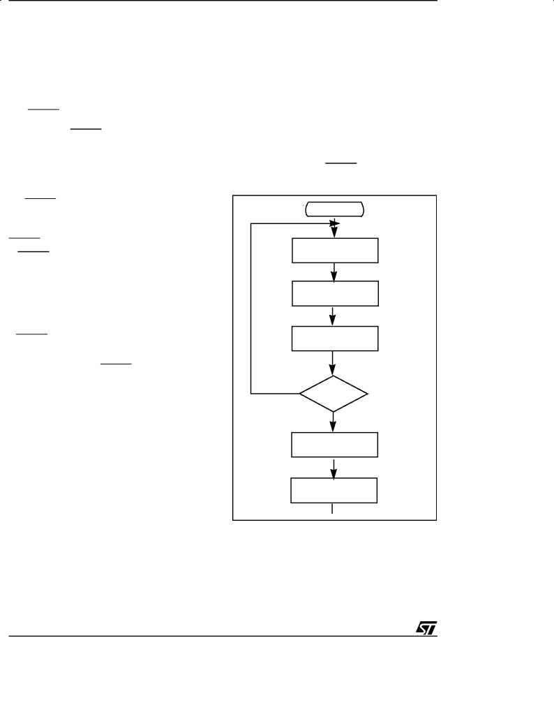
Figure 13. Reset and Interrupt Processing
RESET
NMI MASK SET
INT LATCH CLEARED ( IF PRESENT )
SELECT
NMI MODE FLAGS
PUT FFEH
ON ADDRESS BUS
YES
IS RESET STILL
PRESENT?
NO
LOAD PC
FROM RESET LOCATIONS
FFE/F FF
FETCH INSTRUCTION
VA000427
22/86
ST62T30B ST62E30B
RESETS (Cont'd)
3.2.3 Watchdog Reset
The MCU provides a Watchdog timer function in order to ensure graceful recovery from software upsets. If the Watchdog register is not refreshed before an end-of-count condition is reached, the internal reset will be activated. This, amongst other things, resets the watchdog counter.
The MCU restarts just as though the Reset had been generated by the RESET pin, including the built-in stabilisation delay period.
3.2.4 Application Notes
No external resistor is required between V and
DD
the Reset pin, thanks to the built-in pull-up device.
The POR circuit operates dynamically, in that it triggers MCU initialization on detecting the rising edge of VDD. The typical threshold is in the region of 2 volts, but the actual value of the detected
threshold depends on the way in which V rises.
DD
The POR circuit is NOT designed to supervise static, or slowly rising or falling VDD.
3.2.5 MCU Initialization Sequence
When a reset occurs the stack is reset, the PC is loaded with the address of the Reset Vector (located in program ROM starting at address 0FFEh). A jump to the beginning of the user program must be coded at this address. Following a Reset, the Interrupt flag is automatically set, so that the CPU is in Non Maskable Interrupt mode; this prevents the
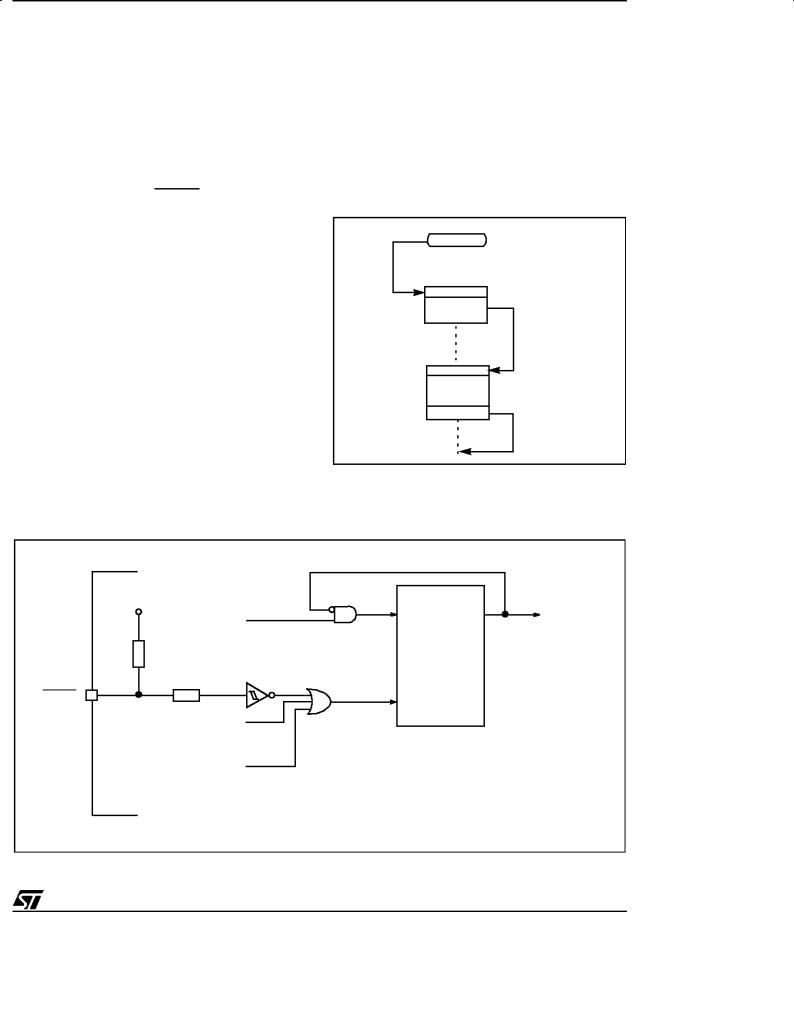
Figure 15. Reset Block Diagram
initialisation routine from being interrupted. The initialisation routine should therefore be terminated by a RETI instruction, in order to revert to normal mode and enable interrupts. If no pending interrupt is present at the end of the initialisation routine, the MCU will continue by processing the instruction immediately following the RETI instruction. If, however, a pending interrupt is present, it will be serviced.
Figure 14. Reset and Interrupt Processing
RESET
JP |
JP:2 BYTES/4 CYCLES |
RESET
VECTOR
INITIALIZATION
ROUTINE |
RETI: 1 BYTE/2 CYCLES |
|
|
|
RETI |
VA00181
VDD |
|
|
ST6 |
fOSC |
|
CK |
|
|
INTERN AL |
||
|
|
|
|
|
|
|
RESET |
300kΩ |
|
COUNTER |
|
RESET |
RESET |
RESET |
|
2.8kΩ |
|
|
|
POWER ON RESET |
|
|
|
WATCHDOG RESET |
|
|
|
|
|
|
VA0200B |
23/86

ST62T30B ST62E30B
RESETS (Cont'd)
Table 7. Register Reset Status
Register |
Address(es) |
Status |
Oscillator Control Register |
0DBh |
|
EEPROM Control Register |
0DFh |
|
Port Data Registers |
0C0h to 0C2h |
|
Port Direction Register |
0C4h to 0C6h |
|
Port Option Register |
0CCh to 0CEh |
|
Interrupt Option Register |
0C8h |
|
TIMER Status/Control |
0D4h |
00h |
|
|
Comment
Main oscillator on
EEPROM enabled
I/O are Input with or without pull-up depending on PORT PULL option
Interrupt disabled
TIMER disabled
AR TIMER Status/Control 1 Register |
0E8h |
|
|
AR TIMER Status/Control 2 Register |
0E1h |
|
|
AR TIMER Status/Control 3 Register |
0E2h |
|
AR TIMER stopped |
AR TIMER Status/Control 4 Register |
OE3h |
|
|
SPI Registers |
0DCh to 0DDh |
|
SPI disabled |
X, Y, V, W, Register |
080H TO 083H |
|
|
Accumulator |
0FFh |
|
|
Data RAM |
084h to 0BFh |
|
|
Data RAM Page REgister |
0CBh |
|
|
Data ROM Window Register |
0C9h |
|
|
EEPROM |
00h to 03Fh |
Undefined |
As written if programmed |
A/D Result Register |
0D0h |
|
|
AR TIMER Capture Register |
0DBh |
|
|
AR TIMER Reload/Capture Register |
0D9h |
|
|
ARTIMER Mask Registers |
OE0h-OEFh |
|
|
ARTIMER Compare Registers |
OEDh-OEEh |
|
|
TIMER Counter Register |
0D3h |
FFh |
|
TIMER Prescaler Register |
0D2h |
7Fh |
Max count loaded |
Watchdog Counter Register |
0D8h |
FEh |
|
A/D Control Register |
0D1h |
40h |
A/D in Stand-by |
UART Control |
OD7h |
|
UART disabled |
UART Data Register |
OD6h |
|
|
|
|
24/86

ST62T30B ST62E30B
3.3 DIGITAL WATCHDOG
The digital Watchdog consists of a reloadable downcounter timer which can be used to provide controlled recovery from software upsets.
The Watchdog circuit generates a Reset when the downcounter reaches zero. User software can prevent this reset by reloading the counter, and should therefore be written so that the counter is regularly reloaded while the user program runs correctly. In the event of a software mishap (usually caused by externally generated interference), the user program will no longer behave in its usual fashion and the timer register will thus not be reloaded periodically. Consequently the timer will decrement down to 00h and reset the MCU. In order to maximise the effectiveness of the Watchdog function, user software must be written with this concept in mind.
Watchdog behaviour is governed by two options, known as ªWATCHDOG ACTIVATIONº (i.e. HARDWARE or SOFTWARE) and ªEXTERNAL STOP MODE CONTROLº (seeTable 8).
In the SOFTWARE option, the Watchdog is disabled until bit C of the DWDR register has been set.
When the Watchdog is disabled, low power Stop mode is available. Once activated, the Watchdog cannot be disabled, except by resetting the MCU.
In the HARDWARE option, the Watchdog is permanently enabled. Since the oscillator will run continuously, low power mode is not available. The STOP instruction is interpreted as a WAIT instruction, and the Watchdog continues to countdown.
However, when the EXTERNAL STOP MODE CONTROL option has been selected low power consumption may be achieved in Stop Mode.
Execution of the STOP instruction is then governed by a secondary function associated with the NMI pin. If a STOP instruction is encountered when the NMI pin is low, it is interpreted as WAIT, as described above. If, however, the STOP instruction is encountered when the NMI pin is high, the Watchdog counter is frozen and the CPU enters STOP mode.
When the MCU exits STOP mode (i.e. when an interrupt is generated), the Watchdog resumes its activity.
Table 8. Recommended Option Choices
Functions Required |
Recommended Optio ns |
Stop Mode & Watchdog |
ªEXTERNAL STOP MODEº & ªHARDWARE WATCHDOGº |
Stop Mode |
ªSOFTWARE WATCHDOGº |
Watchdog |
ªHARDWARE WATCHDOGº |
25/86
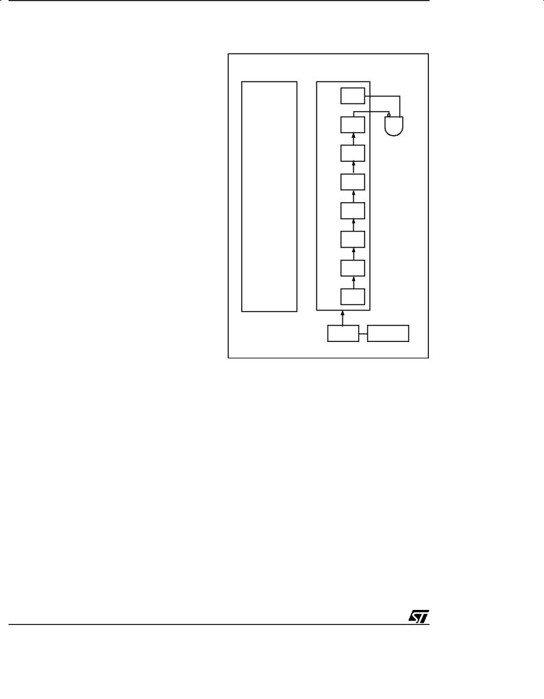
ST62T30B ST62E30B
DIGITAL WATCHDOG (Cont'd)
The Watchdog is associated with a Data space register (Digital WatchDog Register, DWDR, location 0D8h) which is described in greater detail in Section 3.3.1 Digital Watchdog Register (DWDR). This register is set to 0FEh on Reset: bit C is cleared to ª0º, which disables the Watchdog; the timer downcounter bits, T0 to T5, and the SR bit are all set to ª1º, thus selecting the longest Watchdog timer period. This time period can be set to the user's requirements by setting the appropriate value for bits T0 to T5 in the DWDR register. The SR bit must be set to ª1º, since it is this bit which generates the Reset signal when it changes to ª0º; clearing this bit would generate an immediate Reset.
It should be noted that the order of the bits in the DWDR register is inverted with respect to the associated bits in the down counter: bit 7 of the DWDR register corresponds, in fact, to T0 and bit 2 to T5. The user should bear in mind the fact that these bits are inverted and shifted with respect to the physical counter bits when writing to this register. The relationship between the DWDR register bits and the physical implementation of the Watchdog timer downcounter is illustrated inFigure 16.
Only the 6 most significant bits may be used to define the time period, since it is bit 6 which triggers the Reset when it changes to ª0º. This offers the user a choice of 64 timed periods ranging from 3,072 to 196,608 clock cycles (with an oscillator frequency of 8MHz, this is equivalent to timer periods ranging from 384μs to 24.576ms).
Figure 16. Watchdog Counter Control
|
D0 |
|
C |
|
|
|
|
||
REGISTERCONTROLWATCHDOG |
D1 |
|
SR |
|
|
COUNTERWATCHDOG |
|||
D2 |
RESET |
|||
|
|
|||
|
|
T5 |
||
|
D3 |
|
T4 |
|
|
D4 |
|
T3 |
|
|
D5 |
|
T2 |
|
|
D6 |
|
T1 |
|
|
D7 |
|
T0 |
8 |
|
2 |
OSC 12 |
VR02068A
26/86
 Loading...