


ST62T32BQ6
SGS Thomson Microelectronics ST62T32BQ6, ST62T32BQ3, ST62T32BB6, ST62T32BB3, ST62P32BQ6 Datasheet
...
September 1998 1/86
Rev. 2.5
ST62T32B
ST62E32B
8-BIT OTP/EPROM MCUs WITH A/D CONVERTER,
16-BIT AUTO-RELOAD TIMER, EEPROM, SPI AND UART
■ 3.0 to 6.0V Supply Operating Range
■ 8 MHz Maximum Clock Frequency
■
-40 to +125°C Operating Temperature Range
■
Run, Wait and Stop Modes
■ 5 Interrupt Vectors
■ Look-up Table capability in Program Memory
■
Data Storage in Program Memory:
User selectable size
■ Data RAM: 192 bytes
■ Data EEPROM: 128 bytes
■
User Programmable Options
■ 30 I/O pins, fully programmable as:
– Input with pull-up resistor
– Input without pull-up resistor
– Input with interrupt generation
– Open-drain or push-pull output
– Analog Input
■ 9 I/O lines can sinkup to 20mA to drive LEDs or
TRIACs directly
■
8-bit Timer/Counter with 7-bit programmable
prescaler
■ 16-bit Auto-reload Timer with 7-bit
programmable prescaler (AR Timer)
■
Digital Watchdog
■ 8-bit A/D Converter with 21 analog inputs
■ 8-bit Synchronous Peripheral Interface (SPI)
■
8-bit Asynchronous Peripheral Interface
(UART)
■ On-chip Clock oscillator canbedriven by Quartz
Crystal or Ceramic resonator
■
Oscillator Safe Guard
■
One external Non-Maskable Interrupt
■ ST623x-EMU2 Emulation and Development
System (connects to an MS-DOS PC via a
parallel port).
DEVICE SUMMARY
(See end of Datasheet for Ordering Information)
PSDIP42
PQFP52
CDIP42W
DEVICE
OTP
(Bytes)
EPROM
(Bytes)
I/O Pins
ST62T32B 7948 - 30
ST62E32B 7948 30
105

2/86
Table of Contents
86
Document
Page
106
ST62T32B/ST62E32B . . . . . . . . . . . . . . . . . . . . . . . . . . . . . . . . .1
1 GENERAL DESCRIPTION . . . . . . . ...............................................5
1.1 INTRODUCTION .........................................................5
1.2 PIN DESCRIPTIONS . . .. . . . . . . ............................................7
1.3 MEMORYMAP ..........................................................8
1.3.1 Introduction . . . . . . . . ................................................8
1.3.2 Program Space . . . . . . . . . . . . . . . . . . . . . . . . . . . ..........................8
1.3.3 Data Space . . . . . . . . ...............................................10
1.3.4 Stack Space . . . . . . . . . . . . . . . . . ......................................10
1.3.5 Data Window Register (DWR) . . . . . . .. . .. . . . . . . . . . .....................11
1.3.6 Data RAM/EEPROM Bank Register (DRBR)..............................12
1.3.7 EEPROM Description ...............................................13
1.4 PROGRAMMING MODES .................................................15
1.4.1 Option Byte . . . . . . . . ...............................................15
1.4.2 Program Memory . . . . ...............................................15
1.4.3 EEPROM Data Memory . . .. . . . . . . . . ..................................15
1.4.4 EPROMErasing....................................................15
2 CENTRAL PROCESSING UNIT .................................................16
2.1 INTRODUCTION ........................................................16
2.2 CPU REGISTERS . . . . . . . . ...............................................16
3 CLOCKS, RESET, INTERRUPTS AND POWER SAVING MODES . . . . . . . ..............18
3.1 CLOCKSYSTEM........................................................18
3.1.1 Main Oscillator . . . . . . . . . . ...........................................18
3.1.2 Low Frequency Auxiliary Oscillator (LFAO). . . . . . . . . . . . . . . ................19
3.1.3 Oscillator Safe Guard. . . . . . . . . . . . . . . . . . . . . . . . . . . .. . . . ................19
3.2 RESETS...............................................................22
3.2.1 RESET Input ......................................................22
3.2.2 Power-on Reset . . . . . . . . . . . . . . . .....................................22
3.2.3 Watchdog Reset . . . . ...............................................23
3.2.4 Application Notes . . . . ...............................................23
3.2.5 MCU Initialization Sequence ..........................................23
3.3 DIGITAL WATCHDOG . . . . . . . . . . . . . . . .....................................25
3.3.1 Digital Watchdog Register (DWDR). . . ..................................27
3.3.2 Application Notes . . . . ...............................................27
3.4 INTERRUPTS . . . . ......................................................29
3.4.1 Interrupt request . . . . . . . . . . . . . . . .....................................29
3.4.2 Interrupt Procedure . . . ..............................................30
3.4.3 Interrupt Option Register (IOR) . . . . ....................................31
3.4.4 IInterrupt sources . . . . ...............................................31
3.5 POWER SAVING MODES .................................................34
3.5.1 WAIT Mode . . . . . . . . ...............................................34
3.5.2 STOPMode.......................................................34
3.5.3 Exit from WAIT and STOP Modes . . . ...................................35

3/86
Table of Contents
Document
Page
107
4 ON-CHIP PERIPHERALS . . . ...................................................36
4.1 I/OPORTS.............................................................36
4.1.1 Operating Modes . . . . ...............................................37
4.1.2 Safe I/O State Switching Sequence. . . ..................................38
4.1.3 ARTimer alternate functions ..........................................40
4.1.4 SPI alternate functions . . . ............................................40
4.1.5 UART alternate functions . . . . . . . . . . . . . . . . . . . . . . . . . . . . . ................40
4.1.6 I/O Port Option Registers . . . . . . . . . . . . . . . . . . . . . . . . . . . . . ................42
4.1.7 I/O Port Data Direction Registers. . .....................................42
4.1.8 I/O Port Data Registers . . . . ..........................................42
4.2 TIMER ................................................................43
4.2.1 Timer Operating Modes . . .. . . . . . . . . ..................................44
4.2.2 Timer Interrupt . . . . . . . . . . ...........................................44
4.2.3 Application Notes . . . . ...............................................45
4.2.4 Timer Registers . . . . . . . . . . . . . . . . . . . . . . . . . . . .........................45
4.3 ARTIMER 16 . . . ........................................................46
4.3.1 CENTRAL COUNTER . . . ............................................47
4.3.2 SIGNAL GENERATION MODES . . .....................................48
4.3.3 TIMINGS MEASUREMENT MODES. . ..................................50
4.3.4 INTERRUPT CAPABILITIES ..........................................52
4.3.5 CONTROL REGISTERS . . . ..........................................53
4.3.6 16-BIT REGISTERS . . . . . . . . ........................................55
4.4 A/D CONVERTER (ADC) . . . ..............................................57
4.4.1 Application Notes . . . . ...............................................57
4.5 U. A. R. T. (UNIVERSAL ASYNCHRONOUS RECEIVER/TRANSMITTER). ..........59
4.5.1 PORTS INTERFACING . . . . . . . . . . . . ..................................59
4.5.2 CLOCK GENERATION . . . . ..........................................60
4.5.3 DATA TRANSMISSION . . .. . . . . . . . . ..................................60
4.5.4 DATA RECEPTION .................................................61
4.5.5 INTERRUPT CAPABILITIES ..........................................61
4.5.6 REGISTERS ......................................................61
4.6 SERIAL PERIPHERAL INTERFACE (SPI) . . . . . . . . . . . . ........................63
5SOFTWARE ................................................................65
5.1 ST6 ARCHITECTURE . . . . . . . . . . . . . . . .....................................65
5.2 ADDRESSING MODES . . . . ...............................................65
5.3 INSTRUCTION SET . . . ...................................................66
6 ELECTRICAL CHARACTERISTICS. . . . . . . . . . . . ..................................71
6.1 ABSOLUTE MAXIMUM RATINGS. ..........................................71
6.2 RECOMMENDED OPERATING CONDITIONS. . . ..............................72
6.3 DC ELECTRICAL CHARACTERISTICS ......................................73
6.4 AC ELECTRICAL CHARACTERISTICS ......................................74
6.5 A/D CONVERTER CHARACTERISTICS. . . ...................................74
6.6 TIMER CHARACTERISTICS . . . ............................................75
6.7 .SPI CHARACTERISTICS .................................................75
6.8 ARTIMER16 ELECTRICAL CHARACTERISTICS. . . . . . . . . . . . . . . ................75

4/86
Table of Contents
86
Document
Page
108
7 GENERAL INFORMATION . . .. . . . . . . ...........................................76
7.1 PACKAGE MECHANICAL DATA. . . . ........................................76
7.2 ORDERING INFORMATION ...............................................78
ST62P32B . ........................................79
1 GENERAL DESCRIPTION . . . . . . . ..............................................80
1.1 INTRODUCTION ........................................................80
1.2 ORDERING INFORMATION ...............................................80
1.2.1 Transfer of Customer Code . ..........................................80
1.2.2 Listing Generation and Verification . . . . . . . . . . ...........................80
ST6232B . . . . . . . . . . . . . . . . . . . . . . . . . . . . . . . . . . . . . . . . . . .83
1 GENERAL DESCRIPTION . . . . . . . ..............................................84
1.1 INTRODUCTION ........................................................84
1.2 ROM READOUT PROTECTION . . . . . . . . . . . . . . . . . . . . ........................84
1.3 ORDERING INFORMATION ...............................................86
1.3.1 Transfer of Customer Code . ..........................................86
1.3.2 Listing Generation and Verification . . . . . . . . . . ...........................86
5/86
ST62T32B ST62E32B
1 GENERAL DESCRIPTION
1.1 INTRODUCTION
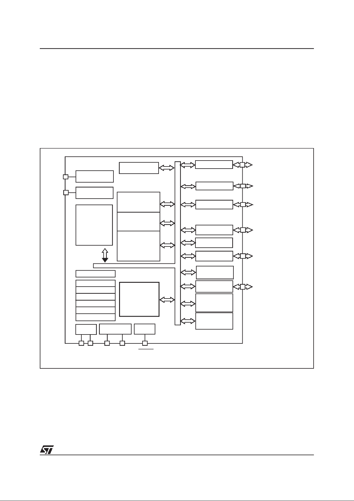
The ST62T32B and ST62E32B devices are low
cost members of the ST62xx 8-bit HCMOS family
of microcontrollers, which is targeted at low to me-
dium complexity applications. All ST62xx devices
are based on a building block approach: a com-
mon core is surrounded by a number of on-chip
peripherals.
The ST62E32B is the erasable EPROM version of
the ST62T32B device, which may be used to em-
ulate the ST62T32B device, as well as the respec-
tive ST6232B ROM devices.
Figure 1. Block Diagram
TEST
NMI INTERRUPT
PROGRAM
PC
STACK LEVEL 1
STACK LEVEL 2
STACK LEVEL 3
STACK LEVEL 4
STACK LEVEL 5
STACK LEVEL 6
POWER
SUPPLY
OSCILLATOR
RESET
DATA ROM
USER
SELECTABLE
DATA RAM
PORT A
PORT B
TIMER
DIGITAL
8 BIT CORE
TEST/V
PP
8-BIT
A/D CONVERTER
PA0..PA1 / 20 mA Sink
V
DD
V
SS
OSCin OSCout RESET
WATCHDOG
Memory
PORT C
SPI (SERIAL
PERIPHERAL
INTERFACE)
AUTORELOAD
TIMER
192 Bytes
7948 bytes
DATA EEPROM
128 Bytes
PA2/OVF/ 20mA Sink
PA3/PWM/20 mA Sink
PA4/Ain/CP1
PA5/Ain/CP2
PB0/Ain
PB3..PB7/Ain
PC5..PC7/Ain
PORT D
PORT E
PD0,PD6,PD7/Ain
PD1/Ain/Scl
PD2/Ain/Sin
PD3/Ain/Sout
PD4/Ain/RXD1
PD5/Ain/TXD1
PE0...PE4
PA6...PA7/Ain
(VPP on EPROM/OTP versions only)
TIMER
VR01823E
UART
109
6/86
ST62T32B ST62E32B
INTRODUCTION (Cont’d)
OTP and EPROM devices are functionally identi-
cal. TheROM based versions offer the same func-
tionality selecting as ROM options the options de-
fined in the programmable option byte of the
OTP/EPROM versions.OTP devices offer all the
advantages of user programmability at low cost,
which make them the ideal choice in a wide range
of applications where frequent code changes, mul-
tiple code versions or last minute programmability
are required.
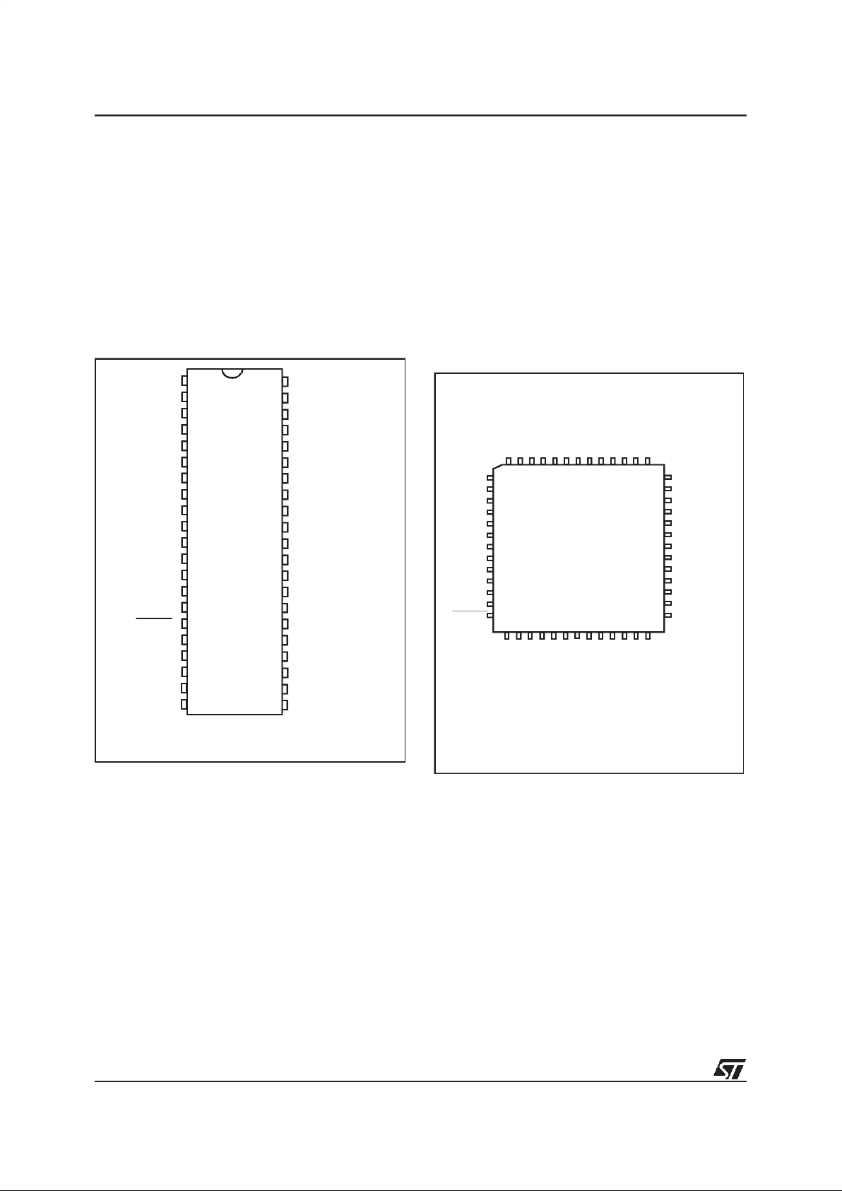
Figure 2. ST62T32B/E32B Pin Configuration
These compact low-cost devices feature a Timer
comprising an 8-bit counter and a 7-bit program-
mable prescaler, an 16-bit Auto-Reload Timer,
with 2 input capture channels, EEPROM data ca-
pability, a serial synchronous port communication
interface (SPI), a serial asynchronous port inter-
face (UART), an 8-bit A/D Converter with 21 ana-
log inputs and a Digital Watchdog timer, making
them well suited for a wide range of automotive,
appliance and industrial applications.
Figure 3. ST62T32B Pin Configuration
1
2
3
4
5
6
7
8
9
10
11
12
13
14
15
16
17
18
19
20
21
PA0
PA1
PA2/OVF
PA3/PWM
PA4/Ain/CP1
PA5/Ain/CP2
PA6/Ain
PA7/Ain
TIMER
NMI
AV
SS
AV
DD
PD0/Ain
PD1/Ain/SCL
PD2/Ain/Sin
PD3/Ain/Sout
PD4/Ain/RXD1
PD5/Ain/TXD1
PD6/Ain
PD7/Ain
PB0/Ain
PE4
PE3
PE2
PE1
PE0
OSCin
OSCout
Ain/CP7
Ain/PC6
Ain/PC5
V
SSp
V
DDp
V
SS
V
DD
TEST/V
PP
(1)
RESET
Ain/PB7
Ain/PB6
Ain/PB5
Ain/PB4
Ain/PB3
42
41
40
39
38
37
36
35
34
33
32
31
30
29
28
27
26
25
24
23
22
1. V
PP
on EPROM/OTP only
VR01375G
1
2
3
4
5
6
7
8
9
10
11
12
13
39
38
37
36
35
34
32
31
30
29
28
27
33
141516171819202122232425
26
52515049484746454443424140
NC
OSCin
OSCout
Ain/PC7
Ain/PC6
Ain/PC5
NC
V
SSP
V
DDP
V
SS
V
DD
TEST/V
PP
(1)
RESET
PA4/Ain/CP1
PA5/Ain/CP2
PA6/Ain
PA7/Ain
TIMER
NMI
AV
SS
AV
DD
PD0/Ain
PD1/Ain/SCL
PD2/Ain/Sin
PD3/Ain/Sout
NC
PE0
PE1
PE2
PE3
PE4
NC
NC
NC
PA0
PA1
PA2/OVF
PA3/PWM
NC
Ain/PB7
Ain/PB6
Ain/PB5
Ain/PB4
Ain/PB3
NC
NC
Ain/PB0
Ain/PD7
Ain/PD6
Ain/PD5/TXD1
Ain/PD4/RXD1
NC
1. V
PP
on EPROM/OTP only
VR02008A
110

7/86
ST62T32B ST62E32B
1.2 PIN DESCRIPTIONS
V
DD
and V
SS
. Power is supplied to the MCU via
these two pins. V
DD
is the power connection and
V
SS
is the ground connection.
V
DDp
and V
SSp
.
Power is supplied to the MCU
I/Os independently from the rest of the chip using
these two pins. These pins have to be connected
to the VDD and VSS pins. It is not allowed to leave
any ofthese pinsunconnected or to applydifferent
potentials respectively to V
DD
/V
DDp
and V
SS
/V
SSp
.
AV
DD
and AV
SS
.
Power is supplied to the
MCUA/D converter independently from the rest of
the chip using these two pins.
OSCin and OSCout. These pins are internally
connected to the on-chip oscillator circuit. A quartz
crystal, a ceramic resonator or an external clock
signal can be connected between these two pins.
The OSCin pin is the input pin, the OSCout pin is
the output pin.
RESET
. The active-low RESET pin is used to re-
start the microcontroller.
TEST/V
PP
. The TEST must be held at V
SS
for nor-
mal operation. If TEST pin is connected to a
+12.5V level during the reset phase, the
EPROM/OTP programming Mode is entered.
NMI.
The NMI pin provides the capability for asyn-
chronous interruption, by applying an external non
maskable interrupt to the MCU.The NMI input is
falling edge sensitive with Schmitt trigger charac-
teristics. The user can select as option the availa-
bility of an on-chip pull-up at this pin.
PA0-PA7. These 8 lines are organised as one I/O
port (A). Each line may be configured under soft-
ware control as inputs with or without internal pull-
up resistors, interrupt generating inputs with pull-
up resistors, open-drain or push-pull outputs.
PA2/OVF, PA3/PWM, PA4/CP1 and PA5/CP2 can
be used respectively as overflow outputpin, output
compare pin, and astwo input capture pins for the
embedded 16-bit Auto-Reload Timer.
In addition, PA4-PA5 can also be used as analog
inputs for the A/D converter while PA0-PA3 can
sink 20mA for direct LED or TRIAC drive.
PB0,PB3-PB7
These 6 lines are organised as one
I/O port (B). Each line may be configured under
software control as inputs with or without internal
pull-up resistors, interrupt generating inputs with
pull-up resistors, open-drain or push-pull outputs,
analog inputs for the A/D converter.
PC5-PC7
. These 3 lines are organised as one I/O
port (C). Each line may be configured under soft-
ware control as input with or without internal pull-
up resistor, interrupt generating input with pull-up
resistor, analog input for the A/D converter, open-
drain or push-pull output.
PD0-PD7. These 8 lines are organised as one I/O
port (portD). Each line may be configured under
software control as input with or without internal
pull-up resistor, interrupt generating input with
pull-up resistor, analog input open-drain or push-
pull output. In adition, the pins PD5/TXD1 and
PD4/RXD1 can be used as UART output
(PD5/TXD1) or UARTinput (PD4/RXD1). The pins
PD3/Sout, PD2/Sin and PD1/SCL can also be
used respectively as data out, data in and Clock
pins for the on-chip SPI.
PE0-PE4. These 5 lines are organised as one I/O
port (PE). Each line may be configured under soft-
ware control as input with or without internal pull-
up resistor, interrupt generation input with pull-up
resistor, open-drain or push-pull output. In output
mode, these lines can also sink 20mA for direct
LED and TRIAC driving.
TIMER. This isthe TIMER 1I/O pin. Ininput mode,
it is connected to the prescaler and acts as ex-
ternal timer clock or as control gate for the internal
timer clock. In output mode, theTIMER pinoutputs
the data bit when a time-out occurs.The user can
select as option the availability of an on-chip pull-
up at this pin.
111
8/86
ST62T32B ST62E32B
1.3 MEMORY MAP
1.3.1 Introduction
The MCU operates in three separate memory
spaces: Program space, Data space, and Stack
space. Operation in these three memory spaces is
described in the following paragraphs.
Briefly, Program space contains user program
code in Program memory and user vectors; Data
space contains user data in RAM and in Program
memory, and Stack space accommodates six lev-
els of stack for subroutine and interrupt service
routine nesting.
1.3.2 Program Space
Program Space comprises the instructions to be
executed, the data required for immediate ad-
dressing mode instructions, the reserved factory
test area and the user vectors. Program Space is
addressed via the 12-bit Program Counter register
(PC register).
Program Space is organised in four 2K pages.
Three of them are addressed in the 000h-7FFh lo-
cations of the Program Space by the Program
Counter and by writing the appropriate code in the
Program ROM Page Register (PRPR register). A
common (STATIC) 2K page is available all the
time for interrupt vectors and common subrou-
tines, independently of the PRPR register content.
This “STATIC” page is directly addressed in the
0800h-0FFFh by the MSB of the Program Counter
register PC 11. Note this page can also be ad-
dressed in the 000-7FFh range. It is two different
ways of addressing the same physical memory.
Jump from a dynamic page to another dynamic
page is achieved by jumping back to the static
page, changing contents of PRPR and then jump-
ing to the new dynamic page.
Figure 4. 8Kbytes Program Space Addressing
Figure 5. Memory Addressing Diagram
PC
SPACE
000h
7FFh
800h
FFFh
0000h
1FFFh
Page 0
Page 1
Static
Page
Page 2 Page 3
Page 1
Static
Page
ROM SPACE
PROGRAM SPACE
PROGRAM
INTERRUPT &
RESET VECTORS
ACCUMULATOR
DATA RAM
BANK SELECT
WINDOW SELECT
RAM
X REGISTER
Y REGISTER
V REGISTER
W REGISTER
DATA READ-ONLY
WINDOW
RAM / EEPROM
BANKING AREA
000h
03Fh
040h
07Fh
080h
081h
082h
083h
084h
0C0h
0FFh
0-63
DATA SPACE
0000h
0FF0h
0FFFh
MEMORY
MEMORY
DATA READ-ONLY
MEMORY
VR01568
112
9/86
ST62T32B ST62E32B
MEMORY MAP (Cont’d)
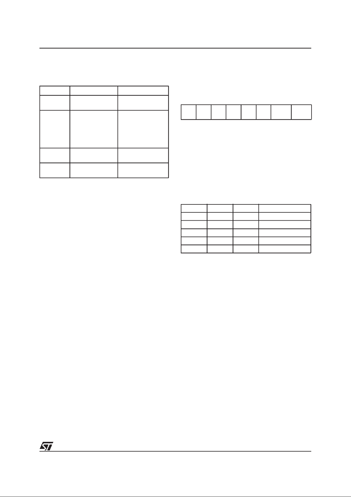
Table 1. ST62E32B/T32B Program Memory Map
Note: OTP/EPROM devices can be programmed
withthe development toolsavailablefrom STMicro-
electronics (ST62E3X-EPB or ST623X-KIT).
1.3.2.1 Program ROM Page Register (PRPR)
The PRPR register can be addressed like a RAM
location in the Data Space at the address CAh ;
nevertheless it is a write only register that cannot
be accessed with single-bit operations. This regis-
ter is used to select the 2-Kbyte ROM bank of the
Program Space that will be addressed. The
number of the page has to be loaded in the PRPR
register. Refer to the Program Space description
for additional information concerning the use of
this register. The PRPR register is not modified
when an interrupt or a subroutine occurs.
Care is required when handling the PRPR register
as it is write only. For this reason, it is not allowed
to change the PRPR contents while executing in-
terrupt service routine, as the service routine
cannot save and then restore its previous content.
This operation may be necessary if common rou-
tines and interrupt service routines take more than
2K bytes ; in this case it could be necessary to di-
vide the interrupt service routine into a (minor) part
in the static page (start and end) and to a second
(major) part in one of the dynamic pages. If it is im-
possible to avoid thewriting of this register in inter-
rupt service routines, an image of this register
must be saved in a RAM location, and each time
the program writes to the PRPR it must write also
to the image register. The image register must be
written before PRPR, so if an interrpt occurs
between the two instructions the PRPR is not af-
fected.
Program ROM Page Register (PRPR)
Address: CAh — Write Only
Bits 2-7= Not used.
Bit 5-0 = PRPR1-PRPR0:
Program ROM Select.
These two bits select the corresponding page to
be addressed in the lower part of the 4K program
address space as specified inTable 2.
This register is undefined on Reset. Neither read
nor single bit instructions may be used to address
this register.
Table 2.8Kbytes Program ROM Page Register
Coding
1.3.2.2 Program Memory Protection
The Program Memory in OTP or EPROM devices
can be protected against external readout of mem-
ory by selecting the READOUT PROTECTION op-
tion in the option byte.
In the EPROM parts, READOUT PROTECTION
option can be disactivated only by U.V. erasure
that also results into the whole EPROM context
erasure.
Note: Once the Readout Protection is activated, it
is no longer possible, even for STMicroelectronics,
to gain access to the Program memory contents.
Returned parts with a protection set can therefore
not be accepted.
ROM Page Device Address Description
Page 0
0000h-007Fh
0080h-07FFh
Reserved
User ROM
Page 1
“STATIC”
0800h-0F9Fh
0FA0h-0FEFh
0FF0h-0FF7h
0FF8h-0FFBh
0FFCh-0FFDh
0FFEh-0FFFh
User ROM
Reserved
Interrupt Vectors
Reserved
NMI Vector
Reset Vector
Page 2
0000h-000Fh
0010h-07FFh
Reserved
User ROM
Page 3
0000h-000Fh
0010h-07FFh
Reserved
User ROM
70
- - - - - - PRPR0 PRPR1
PRPR1 PRPR0 PC bit 11 Memory Page
X X 1 Static Page (Page 1)
0 0 0 Page 0
0 1 0 Page 1 (Static Page
1 0 0 Page 2
1 1 0 Page 3
113

10/86
ST62T32B ST62E32B
MEMORY MAP (Cont’d)
1.3.3 Data Space
Data Space accommodates all the data necessary
for processing the user program. This space com-
prises the RAM resource, the processor core and
peripheral registers, as well as read-only data
such as constants and look-up tables in Program
memory.
1.3.3.1 Data ROM
All read-only data is physically stored in program
memory, which also accommodates the Program
Space. The program memory consequently con-
tains the program code to be executed, as well as
the constants and look-up tables required by the
application.
The Data Space locations in which the different
constants and look-up tables are addressed by the
processor core may be thought of as a 64-byte
window through which it is possible to access the
read-only data stored in Program memory.
1.3.3.2 Data RAM/EEPROM
In ST6232B and ST62E32B devices, the data
space includes 60 bytes of RAM, the accumulator
(A), the indirect registers (X), (Y), the short direct
registers (V), (W), the I/O port registers, the pe-
ripheral data and control registers, the interrupt
option register and the Data ROM Window register
(DRW register).
Additional RAM and EEPROM pages can also be
addressed using banks of 64 bytes located
between addresses 00h and 3Fh.
1.3.4 Stack Space
Stack space consists of six 12-bit registers which
are used to stack subroutine and interrupt return
addresses, as well as the current program counter
contents.
Table 3. Additional RAM/EEPROM Banks.
Table 4. ST62T32B/E32B Data Memory Space
Device RAM EEPROM
ST62T32B/E32B 2 x 64 bytes 2 x 64 bytes
DATAand EEPROM
000h
03Fh
DATA ROM WINDOW AREA
040h
07Fh
X REGISTER 080h
Y REGISTER 081h
V REGISTER 082h
W REGISTER 083h
DATARAM
084h
0BFh
PORT A DATA REGISTER 0C0h
PORT B DATA REGISTER 0C1h
PORT C DATA REGISTER 0C2h
PORT D DATA REGISTER 0C3h
PORT A DIRECTION REGISTER 0C4h
PORT B DIRECTION REGISTER 0C5h
PORT C DIRECTION REGISTER 0C6h
PORT D DIRECTION REGISTER 0C7h
INTERRUPT OPTION REGISTER 0C8h*
DATA ROM WINDOWREGISTER 0C9h*
ROM BANK SELECT REGISTER 0CAh*
RAM/EEPROMBANK SELECTREGISTER 0CBh*
PORT A OPTION REGISTER 0CCh
PORT B OPTION REGISTER 0CDh
PORT C OPTION REGISTER 0CEh
PORT D OPTION REGISTER 0CFh
A/D DATA REGISTER 0D0h
A/D CONTROL REGISTER 0D1h
TIMER 1 PRESCALER REGISTER 0D2h
TIMER 1 COUNTER REGISTER 0D3h
TIMER 1 STATUS/CONTROLREGISTER 0D4h
RESERVED 0D5h
UART DATASHIFT REGISTER 0D6h
UARTSTATUS CONTROL REGISTER 0D7h
WATCHDOG REGISTER 0D8h
RESERVED 0D9h
I/O INTERRUPT POLARITY REGISTER 0DAh
OSCILLATOR CONTROL REGISTER 0DBh
SPI INTERRUPT DISABLEREGISTER 0DCh*
SPI DATA REGISTER 0DDh
RESERVED 0DEh
EEPROM CONTROL REGISTER 0DFh
ARTIM16 COMPAREMASK REG. LOW BYTE MASK 0E0h
ARTIM16 2ND STATUSCONTROL REGISTERSCR2 0E1h
ARTIM16 3RD STATUSCONTROL REGISTERSCR3 0E2h
ARTIM16 4TH STATUSCONTROL REGISTER SCR4 0E3h
ARTIM16 1ST STATUSCONTROL REGISTER SCR1 0E8h
ARTIM16 RELOAD CAPTURE REG. HIGH BYTE RLCP 0E9h
ARTIM16 RELOAD CAPTURE REG. LOW BYTE RLCP 0EAh
ARTIM16 CAPTURE REGISTER HIGH BYTECP 0EBh
ARTIM16 CAPTURE REGISTER LOW BYTE CP 0ECh
ARTIM16COMPAREVALUE REGISTERHIGHBYTECMP 0EDh
ARTIM16COMPAREVALUEREGISTERLOWBYTECMP 0EEh
ARTIM 16 COMPARE MASK REG. HIGH BYTE MASK 0EFh
RESERVED 0F0h
0FBh
PORT E DATA REGISTER OFCh
PORT E DIRECTION REGISTER 0FDh
PORT E OPTION REGISTER 0FEh
ACCUMULATOR OFFh
* WRITE ONLY REGISTER
114
11/86
ST62T32B ST62E32B
MEMORY MAP (Cont’d)
1.3.5 Data Window Register (DWR)
The Dataread-only memory window is locatedfrom
address 0040h to address 007Fh in Data space. It
allows direct reading of 64 consecutive bytes locat-
ed anywhere in program memory, between ad-
dress 0000h and 1FFFh (top memory address de-
pends on the specific device). All the program
memory can therefore be used to store either in-
structions or read-only data. Indeed, the window
can be moved in steps of 64 bytes along the pro-
grammemory by writingtheappropriate codeinthe
Data Window Register (DWR).
The DWRcan be addressed like any RAM location
in the Data Space, it is however a write-only regis-
ter and therefore cannot be accessed using single-
bit operations. This register is used to position the
64-byte read-only data window (from address 40h
to address 7Fh of the Data space) in program
memory in 64-byte steps. The effective address of
the byte to be read as data in program memory is
obtained by concatenating the 6 least significant
bits of the register address given in the instruction
(as least significant bits) and the content of the
DWR register (as most significantbits), as illustrat-
ed in Figure 6below. For instance, when address-
ing location 0040h of the Data Space, with 0 load-
ed in the DWR register, the physical location ad-
dressed in program memory is 00h. The DWR reg-
ister is not cleared on reset, therefore it must be
written to prior tothe first access to the Data read-
only memory window area.
Data Window Register (DWR)
Address: 0C9h — Write Only
Bits 7 = Not used.
Bit 6-0 =
DWR5-DWR0:
Data read-only memory
Window Register Bits.
These are the Data read-
only memory Window bits that correspond to the
upper bits of the data read-only memory space.
Caution:
This register is undefined on reset. Nei-
ther read nor single bit instructions may beused to
address this register.
Note:
Care is required when handling the DWR
register as it is write only. For this reason, the
DWR contents should not be changed while exe-
cuting an interrupt service routine, as the service
routine cannot save and then restore the register’s
previous contents. If it is impossible to avoid writ-
ing to theDWR during the interrupt service routine,
an image of the register must be saved in a RAM
location, and each time the program writes to the
DWR, it must also write to the image register. The
image register must be written first so that, if an in-
terrupt occurs between the two instructions, the
DWR is not affected.
Figure 6. Data read-only memory Window Memory Addressing
70
- DWR6 DWR5 DWR4 DWR3 DWR2 DWR1 DWR0
DATA ROM
WINDOW REGISTER
CONTENTS
DATA SPACE ADDRESS
40h-7Fh
IN INSTRUCTION
PROGRAM SPACE ADDRESS
765432 0
543210
543210
READ
1
67891011
0
1
VR0A1573
12
1
0
DATA SPACE ADDRESS
59h
0000
0
1
00
1
11
Example:
(DWR)
DWR=28h
11000000001
ROM
ADDRESS:A19h
11
13
01
115

12/86
ST62T32B ST62E32B
MEMORY MAP (Cont’d)
1.3.6 Data RAM/EEPROM Bank Register
(DRBR)
Address: CBh — Write only
Bit 7-5 = These bits are not used
Bit 4 - DRBR4. This bit, when set, selects RAM
Page 2.
Bit 3 - DRBR3. This bit, when set, selects RAM
Page 1.
Bit2. This bit is not used.
Bit 1 - DRBR1. This bit, when set, selects
EEPROM Page 1.
Bit 0 - DRBR0. This bit, when set, selects
EEPROM Page 0.
The selection of the bank ismade byprogramming
the Data RAM Bank Switch register (DRBR regis-
ter) located at address CBh of the Data Space ac-
cording to Table 1. No more than one bank should
be set at a time.
The DRBR register can be addressed like a RAM
Data Space at the address CBh; nevertheless it is
a write only register that cannot be accessed with
single-bit operations. This register is used to select
the desired 64-byte RAM/EEPROM bank of the
Data Space. The number of banks has to be load-
ed in the DRBR register and the instruction has to
point to the selected location as if it was in bank 0
(from 00h address to 3Fh address).
This register is not cleared during the MCU initiali-
zation, therefore it must be written before the first
access to the Data Space bank region. Refer to
the Data Space description for additional informa-
tion. The DRBR register is not modified when an
interrupt or a subroutine occurs.
Notes :
Care isrequired when handling the DRBR register
as it is write only. For this reason, it is not allowed
to change the DRBR contents while executing in-
terrupt service routine, as the service routine can-
not save and then restore its previous content. If it
is impossible to avoid the writing of this register in
interrupt service routine, an image of this register
must be saved in a RAM location, and each time
the program writes to DRBR it must write also to
the image register. The image register must be
written first, so if an interrupt occurs between the
two instructions the DRBR is not affected.
In DRBR Register, only 1 bit must be set. Other-
wise two or more pages are enabled in parallel,
producing errors.
Table 5. Data RAM Bank Register Set-up
70
- - - DRBR4 DRBR3 - DRBR1 DRBR0
DRBR ST62T32B/E32B
00 None
01 EEPROM Page 0
02 EEPROM Page 1
08 RAM Page 1
10h RAM Page2
other Reserved
116

13/86
ST62T32B ST62E32B
MEMORY MAP (Cont’d)
1.3.7 EEPROM Description
EEPROM memory is located in 64-byte pages in
data space. This memory may be used by the user
program for non-volatile data storage.
Data space from 00h to 3Fh is paged as described
in Table 6. EEPROM locations are accessed di-
rectly by addressing these paged sections of data
space.
The EEPROM does not require dedicated instruc-
tions for read orwriteaccess.Once selected via the
Data RAM Bank Register, the active EEPROM
page is controlled bythe EEPROM Control Regis-
ter (EECTL), which is described below.
BitE20FF oftheEECTLregister mustbereset prior
to any write or read access to the EEPROM. If no
bank hasbeenselected, orifE2OFF is set,any ac-
cess is meaningless.
Programming must be enabled by setting the
E2ENA bit of the EECTL register.
The E2BUSYbit of the EECTL register is setwhen
the EEPROM is performing a programming cycle.
Any access to the EEPROM when E2BUSY is set
is meaningless.
Provided E2OFF and E2BUSY are reset, an EEP-
ROM location is read just like any other data loca-
tion, also in terms of access time.
Writing to the EEPROM may be carried out in two
modes: Byte Mode (BMODE) and Parallel Mode
(PMODE). In BMODE, one byte is accessed at a
time, while in PMODE up to 8 bytes in the same
row are programmed simultaneously (with conse-
quent speed and power consumption advantages,
the latter being particularly important in battery
powered circuits).
General Notes:
Data should be written directly to the intended ad-
dress in EEPROM space. There is no buffer mem-
ory between data RAM and the EEPROM space.
When the EEPROM is busy (E2BUSY = “1”)
EECTL cannot be accessed in write mode, it is
only possible to read the status of E2BUSY. This
implies that as long as the EEPROM is busy, it is
not possible to change the status of the EEPROM
Control Register. EECTL bits 4 and 5 are reserved
and must never be set.
Care is requiredwhen dealing with the EECTL reg-
ister, as some bits are write only. For this reason,
the EECTL contents must not be altered while ex-
ecuting an interrupt service routine.
If it is impossible to avoid writing to this register
within an interrupt service routine, an image of the
register must be saved in a RAM location, and
each time the program writes to EECTL it must
also writeto the image register. The image register
must be written to first so that, if an interrupt oc-
curs between the two instructions, the EECTL will
not be affected.
Table 6. Row Arrangement for Parallel Writing of EEPROM Locations
Dataspace
addresses.
Banks 0 and 1.
Byte 01234567
ROW7 38h-3Fh
ROW6 30h-37h
ROW5 28h-2Fh
ROW4 20h-27h
ROW3 18h-1Fh
ROW2 10h-17h
ROW1 08h-0Fh
ROW0 00h-07h
Up to 8 bytes in each row may be programmed simultaneously in Parallel Write mode.
The number of available 64-byte banks (1 or 2) is device dependent.
117

14/86
ST62T32B ST62E32B
MEMORY MAP (Cont’d)
Additional Notes on Parallel Mode:
If the user wishes to perform parallel program-
ming, the first step should be to set the E2PAR2
bit. From this time on, the EEPROM will be ad-
dressed in write mode, the ROW address will be
latched and it will be possible to change it only at
the end of the programming cycle, or by resetting
E2PAR2 without programming the EEPROM. Af-
ter the ROW address is latched, the MCU can only
“see” the selected EEPROM row and any attempt
to write or read other rows will produce errors.
The EEPROM should not be read while E2PAR2
is set.
As soon as the E2PAR2 bit is set, the 8 volatile
ROW latches are cleared. From this moment on,
the user can load data in all or in part of the ROW.
Setting E2PAR1 will modify the EEPROM regis-
ters corresponding to the ROW latches accessed
after E2PAR2. For example, if the software sets
E2PAR2 and accesses the EEPROM by writing to
addresses 18h, 1Ah and 1Bh, and then sets
E2PAR1, these three registers will be modified si-
multaneously; the remaining bytes in the row will
be unaffected.
Note that E2PAR2 is internally reset at the end of
the programming cycle. This implies that the user
must set the E2PAR2 bit between two parallel pro-
gramming cycles. Note that if the user tries to set
E2PAR1 while E2PAR2 is not set, there will be no
programming cycle and theE2PAR1 bit will be un-
affected. Consequently, the E2PAR1 bit cannot be
set if E2ENA is low. The E2PAR1 bit can be set by
the user, only if the E2ENA and E2PAR2 bits are
also set.
EEPROM Control Register (EECTL)
Address: DFh — Read/Write
Reset status: 00h
Bit 7 = D7:
Unused.
Bit6=E2OFF:
Stand-by Enable Bit.
WRITE ONLY.
Ifthisbitis settheEEPROMisdisabled(any access
willbemeaningless) andthepowerconsumption of
the EEPROM is reduced to its lowest value.
Bit 5-4 =D5-D4:
Reserved.
MUST be kept reset.
Bit 3 =
E2PAR1
:
Parallel Start Bit.
WRITE ONLY.
OnceinParallelMode,assoonastheusersoftware
sets the E2PAR1 bit, parallel writing of the 8 adja-
cent registers will start. This bitisinternally reset at
the end of the programming procedure. Note that
less than 8 bytes can bewritten ifrequired, the un-
defined bytes being unaffected by the parallel pro-
gramming cycle; this is explained in greater detail in
the Additional Notes on Parallel Mode overleaf.
Bit 2 = E2PAR2:
Parallel Mode En. Bit.
WRITE
ONLY. This bit must be setby the user program in
order to perform parallel programming. If E2PAR2
is set and the parallel start bit (E2PAR1) is reset,
up to 8 adjacent bytes can be written simultane-
ously. These 8 adjacent bytes are considered as a
row, whose address lines A7, A6, A5, A4, A3 are
fixed while A2, A1andA0 arethe changing bits, as
illustrated in Table 6. E2PAR2 is automatically re-
set at the end of any parallel programming proce-
dure. It can be reset by the user software before
starting the programming procedure, thus leaving
the EEPROM registers unchanged.
Bit 1 = E2BUSY:
EEPROM Busy Bit.
READ ON-
LY. This bit is automatically set by the EEPROM
control logic when the EEPROM is in program-
ming mode. The user program should test it before
any EEPROM read or write operation; any attempt
to access the EEPROM while the busy bit is set
will be aborted and the writing procedure in
progress will be completed.
Bit 0 =
E2ENA
:
EEPROM Enable Bit.
WRITE ON-
LY. This bit enables programming of the EEPROM
cells. It must be set before any write to the EEP-
ROM register. Any attempt to write to the EEP-
ROM when E2ENA is low is meaningless and will
not trigger a write cycle.
70
D7 E2OFF D5 D4 E2PAR1 E2PAR2 E2BUSY E2ENA
118

15/86
ST62T32B ST62E32B
1.4 PROGRAMMING MODES
1.4.1 Option Byte
The Option Byte allows configuration capability to
the MCUs. Option byte’s content is automatically
read, and the selected options enabled, when the
chip reset is activated.
It can only be accessed during the programming
mode. This access is made either automatically
(copy from a master device) or by selecting the
OPTION BYTE PROGRAMMING mode ofthe pro-
grammer.
The option byte is located in a non-user map. No
address has to be specified.
EPROM Code Option Byte
Bit 7. Reserved.
Bit 6 =
PORT PULL
. This bit must be set high to
have pull-up input state at reset on the I/O port.
When this bit is low, I/O ports are in input without
pull-up (high impedance) state at reset
Bit 5 =
EXTCNTL
. This bit selects the External
STOP Mode capability. When EXTCNTL is high,
pin NMI controls if the STOP mode can be ac-
cessed when the watchdog is active. When EXTC-
NTL is low, the STOP instruction is processed as a
WAIT as soon as the watchdog is active.
Bit 4 = PROTECT. This bit allows the protection of
the software contents against piracy. When the bit
PROTECT is set high, readout of the OTP con-
tents is prevented by hardware. No programming
equipment is able to gain access to the user pro-
gram. When this bit is low, the user program can
be read.
Bit 3 =TIM PULL.This bit must be set high tocon-
figure the TIMER pin with a pull up resistor. When
it is low, no pull up is provided.
Bit 2 =NMI PULL. This bit mustbe set high tocon-
figure the NMI pin with a pull up resistor when it is
low, no pull up is provided.
Bit 1 = WDACT. This bit controls the watchdog ac-
tivation. When it is high, hardware activation is se-
lected. The software activation is selected when
WDACT is low.
Bit 0 =OSGEN.This bit must be set high to enable
the oscillator Safe Guard. When this bit is low, the
OSG is disabled.
The Option byte is written during programming ei-
ther by using the PC menu (PC driven Mode) or
automatically (stand-alone mode)
1.4.2 Program Memory
EPROM/OTP programming mode is set by a
+12.5V voltage applied to the TEST/V
PP
pin. The
programming flow of the ST62T32B/E32B is de-
scribed in the User Manual of the EPROM Pro-
gramming Board.
The MCUs can be programmed with the
ST62E3xB EPROM programming tools available
from STMicroelectronics.
1.4.3 EEPROM Data Memory
EEPROM data pages are supplied in the virgin
state FFh. Partial or total programming of EEP-
ROM data memory can be performed either
through the application software, or through an ex-
ternal programmer. Any STMicroelectronics tool
used for the program memory (OTP/EPROM) can
also be used to program the EEPROM data mem-
ory.
1.4.4 EPROM Erasing
The EPROM of the windowed package of the
MCUs may be erased by exposure to Ultra Violet
light. The erasure characteristic of the MCUs is
such that erasure begins when the memory is ex-
posed to light with a wave lengths shorter than ap-
proximately 4000Å. It should be noted that sun-
lights and some types of fluorescent lamps have
wavelengths in the range 3000-4000Å.
It is thus recommended that the window of the
MCUs packages becovered by an opaque label to
prevent unintentional erasure problems when test-
ing the application in such an environment.
The recommended erasure procedure of the
MCUs EPROM is the exposure to short wave ul-
traviolet light which have a wave-length 2537A.
The integrated dose (i.e. U.V. intensity x exposure
time) for erasure should be a minimum of 15W-
sec/cm
2
. The erasure time with this dosage is ap-
proximately 15 to 20 minutes using an ultraviolet
lamp with 12000µW/cm
2
power rating. The
ST62E32B should be placed within 2.5cm (1Inch)
of the lamp tubes during erasure.
70
-
PORT
PULL
EXTCNTLPROTECT
TIM
PULL
NMI
PULL
WDACT OSGEN
119
16/86
ST62T32B ST62E32B
2 CENTRAL PROCESSING UNIT
2.1 INTRODUCTION
The CPUCoreofST6devicesisindependent ofthe
I/O or Memory configuration. As such, it may be
thought of as an independent central processor
communicating with on-chip I/O, Memory and Pe-
ripherals via internal address, data, and control
buses. In-core communication is arranged as
shown in Figure 7; the controller being externally
linked to both the Reset and Oscillator circuits,
while the core islinked to the dedicated on-chip pe-
ripherals via the serial data bus and indirectly, for
interrupt purposes, through the control registers.
2.2 CPU REGISTERS
TheST6FamilyCPUcorefeaturessixregistersand
three pairs of flags available to the programmer.
These are described in the following paragraphs.
Accumulator (A). The accumulator is an 8-bit
general purpose register used in all arithmetic cal-
culations, logical operations, and data manipula-
tions. The accumulator can be addressed in Data
space asa RAM location ataddress FFh. Thus the
ST6 can manipulate the accumulator just like any
other register in Data space.
Indirect Registers (X, Y).These two indirect reg-
isters are used as pointers to memory locations in
Data space. They are used in the register-indirect
addressing mode. These registers can be ad-
dressed in the data space as RAM locations at ad-
dresses 80h (X) and 81h (Y). They can also be ac-
cessed with the direct, shortdirect, or bit direct ad-
dressing modes. Accordingly, the ST6 instruction
set can use the indirect registers as any other reg-
ister of the data space.
Short Direct Registers (V, W).These two regis-
ters are used to save a byte in short direct ad-
dressing mode. They can be addressed in Data
space as RAM locations at addresses 82h (V) and
83h (W). They can also be accessed using the di-
rect and bit direct addressing modes. Thus, the
ST6 instruction set can use the short direct regis-
ters as any other register of the data space.
Program Counter (PC). The program counter is a
12-bit register which contains the address of the
next ROM location to be processed by the core.
This ROM location may be an opcode, an oper-
and, or the address of an operand. The 12-bit
length allows the direct addressing of 4096 bytes
in Program space.
Figure 7. ST6 Core Block Diagram
PROGRAM
RESET
OPCODE
FLAG
VALUES
2
CONTROLLER
FLAGS
ALU
A-DATA
B-DATA
ADDRESS/READ LINE
DATA SPACE
INTERRUPTS
DATA
RAM/EEPROM
DATA
ROM/EPROM
RESULTS TO DATA SPACE (WRITE LINE)
ROM/EPROM
DEDICATIONS
ACCUMULATOR
CONTROL
SIGNALS
OSCin
OSCout
ADDRESS
DECODER
256
12
Program Counter
and
6 LAYER STACK
0,01 TO 8MHz
VR01811
120
17/86
ST62T32B ST62E32B
CPU REGISTERS (Cont’d)
However, ifthe program space contains more than
4096 bytes, the additional memory in program
space can be addressed by using the Program
Bank Switch register.
The PC value is incremented after reading the ad-
dress of the current instruction. To execute relative
jumps, the PC and the offset are shifted through
the ALU, where they are added; the result is then
shifted back into the PC. The program counter can
be changed in the following ways:
- JP (Jump) instructionPC=Jump address
- CALL instructionPC= Call address
- Relative Branch Instruction.PC= PC +/- offset
- Interrupt PC=Interrupt vector
- Reset PC= Reset vector
- RET & RETI instructionsPC= Pop (stack)
- Normal instructionPC= PC + 1
Flags (C, Z). The ST6 CPU includes three pairs of
flags (Carry and Zero), each pairbeing associated
with one of the three normal modes of operation:
Normal mode, Interrupt mode and Non Maskable
Interrupt mode. Each pair consists of a CARRY
flag and a ZERO flag. One pair (CN, ZN) is used
during Normal operation, another pair is used dur-
ing Interrupt mode (CI, ZI), and a third pair is used
in the Non Maskable Interrupt mode (CNMI, ZN-
MI).
The ST6 CPU uses the pair of flags associated
with the current mode: as soon as an interrupt (or
a Non Maskable Interrupt) is generated, the ST6
CPU uses the Interrupt flags (resp. the NMI flags)
instead of the Normal flags. When the RETI in-
struction is executed, the previously used set of
flags is restored. It should be noted that each flag
set can only be addressed in its own context (Non
Maskable Interrupt, Normal Interrupt or Main rou-
tine). The flags are not cleared during context
switching and thus retain their status.
The Carry flag is set when a carry or a borrow oc-
curs during arithmetic operations; otherwise it is
cleared. The Carry flag is also set to the value of
the bit tested in a bit test instruction; it also partici-
pates in the rotate left instruction.
The Zero flag is set if the result of the last arithme-
tic or logical operation was equal to zero; other-
wise it is cleared.
Switching between the three sets of flags is per-
formed automatically when an NMI, an interrupt or
a RETI instructions occurs. As the NMI mode is
automatically selected after the reset of the MCU,
the ST6 core uses at first the NMI flags.
Stack. The ST6 CPU includes a true LIFO hard-
ware stack which eliminates the need for a stack
pointer. The stack consists of six separate 12-bit
RAM locations that do not belong to the data
space RAM area. When a subroutine call (or inter-
rupt request) occurs, the contents of each level are
shifted into the next higher level, while the content
of the PC is shifted into the first level (the original
contents of the sixth stack level are lost). When a
subroutine or interrupt return occurs (RETor RETI
instructions), the first level register is shifted back
into the PC and the value of each level is popped
back into the previous level. Since the accumula-
tor, in common with all other data space registers,
is not stored in this stack, management of these
registers should be performed within the subrou-
tine. The stack will remain in its “deepest” position
if more than 6 nested calls or interrupts are execut-
ed, and consequently the last return address will
be lost. It will also remain in its highest position if
the stack is empty and a RET or RETI is executed.
In this case the next instruction will be executed.
Figure 8. ST6 CPU Programming Mode
l
SHORT
DIRECT
ADDRESSING
MODE
V REGISTER
WREGISTER
PROGRAM COUNTER
SIX LEVELS
STACK REGISTER
CZNORMAL FLAGS
INTERRUPT FLAGS
NMI FLAGS
INDEX
REGISTER
VA000423
b7
b7
b7
b7
b7
b0
b0
b0
b0
b0
b0b11
ACCUMULATOR
YREG.POINTER
XREG.POINTER
CZ
CZ
121
18/86
ST62T32B ST62E32B
3 CLOCKS, RESET, INTERRUPTS AND POWER SAVING MODES
3.1 CLOCK SYSTEM
The MCU features a Main Oscillator which can be
driven by an external clock, or used in conjunction
with an AT-cut parallel resonant crystal or a suita-
ble ceramic resonator. In addition, a Low Frequen-
cy Auxiliary Oscillator (LFAO) can be switched in
for security reasons, to reduce power consump-
tion, or to offer the benefits of a back-up clock sys-
tem.
The Oscillator Safeguard (OSG) option filters
spikes from the oscillator lines, provides access to
the LFAO to provide a backup oscillator in the
event of main oscillator failure and also automati-
cally limits the internal clock frequency (f
INT
)asa
function ofV
DD
, in order to guarantee correct oper-
ation. These functions are illustrated in Figure 10,
Figure 11, Figure 12 and Figure 13.
Figure 9 illustrates various possible oscillator con-
figurations using anexternal crystalorceramic res-
onator, anexternal clockinputorthelowestcostso-
lution using onlytheLFAO.C
L1
an C
L2
should have
acapacitance intherange12to22pFforanoscillator
frequency in the 4-8 MHz range.
The internal MCU clock frequency (f
INT
) is divided
by 12 to drive the Timer and the Watchdog timer,
and by 13 to drive the CPU core, while the A/D
converter is driven by f
INT
divided either by 6 or by
12 as may be seen in Figure 12.
With an 8MHz oscillator frequency, thefastest ma-
chine cycle is therefore 1.625µs.
A machine cycleis the smallest unit oftime needed
toexecute any operation (for instance, to increment
the Program Counter). An instruction may require
two, four, or five machine cycles for execution.
3.1.1 Main Oscillator
The main oscillator can be turned off (when the
OSG ENABLED option is selected) by setting the
OSCOFF bit of the OSCR Control Register. The
Low Frequency Auxiliary Oscillator is automatical-
ly started.
Figure 9. Oscillator Configurations
INTEGRATEDCLOCK
OSG ENABLED option
OSC
in
OSC
out
C
L1n
C
L2
ST6xxx
CRYSTAL/RESONATOR CLOCK
OSC
in
OSC
out
ST6xxx
EXTERNAL CLOCK
NC
OSC
in
OSC
out
ST6xxx
NC
VA0016
VA0015A
122

19/86
ST62T32B ST62E32B
CLOCK SYSTEM (Cont’d)
Turning on the main oscillator is achieved by re-
setting the OSCOFF bit of the OSCR Register or
by resetting the MCU. Restarting the main oscilla-
tor implies a delay comprising the oscillator start
up delay period plus the duration of the software
instruction at f
LFAO
clock frequency.
3.1.2 Low Frequency Auxiliary Oscillator
(LFAO)
The Low Frequency Auxiliary Oscillator has three
main purposes. Firstly, it can be used to reduce
power consumption in non timing critical routines.
Secondly, it offers a fully integrated system clock,
without any external components. Lastly, it acts as
a safety oscillator in case of main oscillator failure.
This oscillator is available when the OSG ENA-
BLED option is selected. In this case, it automati-
cally starts one of its periods after the first missing
edge from the main oscillator, whatever the reason
(main oscillator defective, no clock circuitry provid-
ed, main oscillator switched off...).
User code, normal interrupts, WAIT and STOP in-
structions, are processed as normal, at the re-
duced f
LFAO
frequency. The A/D converter accura-
cy is decreased, since theinternal frequency isbe-
low 1MHz.
At power on, the Low Frequency Auxiliary Oscilla-
tor starts faster than the Main Oscillator. It there-
fore feeds the on-chip counter generating thePOR
delay until the Main Oscillator runs.
The Low Frequency Auxiliary Oscillator is auto-
matically switched off as soon as the main oscilla-
tor starts.
OSCR
Address: 0DBh — Read/Write
Bit 7-1= These bits are not used and must be kept
cleared after reset.
Bit 0 =
OSCOFF
.
Main oscillator turn-off.
When
low, this bit enables main oscillator to run. The
main oscillator is switched off when OSCOFF is
high.
3.1.3 Oscillator Safe Guard
The Oscillator Safe Guard (OSG) affords drastical-
ly increased operational integrity in ST62xx devic-
es. The OSG circuit provides three basic func-
tions: it filters spikes from the oscillator lines which
would result in over frequency to the ST62 CPU; it
gives access to the Low Frequency Auxiliary Os-
cillator (LFAO), used to ensure minimum process-
ing in case of main oscillator failure, to offer re-
duced power consumption or to provide a fixed fre-
quency low cost oscillator; finally, it automatically
limits the internal clock frequency as a function of
supply voltage, in order to ensure correct opera-
tion even if the power supply should drop.
The OSG is enabled or disabled by choosing the
relevant OSG option. It may be viewed as a filter
whose cross-over frequency is device dependent.
Spikes on the oscillator linesresult in aneffectively
increased internal clock frequency. In the absence
of an OSG circuit, this may lead to an over fre-
quency for a given power supply voltage. The
OSG filters out such spikes (as illustrated in Fig-
ure 10). In all cases, when the OSG is active, the
maximum internal clock frequency, f
INT
, is limited
to f
OSG
, which is supply voltage dependent. This
relationship is illustrated in Figure 13.
When the OSG is enabled, the Low Frequency
Auxiliary Oscillator may be accessed. This oscilla-
tor starts operating after the first missing edge of
the main oscillator (see Figure 11).
Over-frequency, at a given power supply level, is
seen by the OSG as spikes; it therefore filters out
some cycles in order that the internal clock fre-
quency of the device is kept within the range the
particular device can stand (depending on V
DD
),
and below f
OSG
: the maximum authorised frequen-
cy with OSG enabled.
Note. The OSGshould beused whereverpossible
as it provides maximum safety. Care must be tak-
en, however, as it can increase power consump-
tion and reduce the maximum operating frequency
to f
OSG
.
70
-------
OSC
OFF
123

20/86
ST62T32B ST62E32B
CLOCK SYSTEM (Cont’d)
Figure 10. OSG Filtering Principle
Figure 11. OSG Emergency Oscillator Principle
(1)
VR001932
(3)
(2)
(4)
(1)
(2)
(3)
(4)
Maximum Frequency for the device to work correctly
Actual Quartz Crystal Frequency at OSCin pin
Noise from OSCin
Resulting Internal Frequency
Main
VR001933
Internal
Emergency
Oscillator
Frequency
Oscillator
124

21/86
ST62T32B ST62E32B
CLOCK SYSTEM (Cont’d)
Figure 12. Clock Circuit Block Diagram
Figure 13. Maximum Operating Frequency (f
MAX
) versus Supply Voltage (V
DD
)
Notes
:
1. In this area, operation is guaranteed at the quartz crystal frequency.
2. Whenthe OSG isdisabled, operation in this area is guaranteed atthe crystalfrequency. When the OSG
is enabled, operation in this area is guaranteed at a frequency of at least f
OSG Min.
3. When the OSG is disabled, operation in this area is guaranteed at the quartz crystal frequency. When
the OSG is enabled, access to this area is prevented. The internal frequency is kept a f
OSG.
4. When the OSG is disabled, operation in this area is not guaranteed
When the OSG is enabled, access to this area is prevented. The internal frequency is kept at f
OSG.
MAIN
OSCILLATOR
OSG
LFAO
M
U
X
Core
:13
:12
:1
TIMER 1
Watchdog
POR
f
INT
Main Oscillator off
ADC
ARTIMER 16
:6
M
U
X
1
2.5
3.5 4 4.5 5 5.5 6
8
7
6
5
4
3
2
Maximum FREQUENCY (MHz)
SUPPLY VOLTAGE (V
DD
)
FUNCTIONALITY IS NOT
3
4
3
2
1
f
OSG
f
OSG
Min
GUARANTEED
IN THIS AREA
VR01807
125
22/86
ST62T32B ST62E32B
3.2 RESETS
The MCU can be reset in three ways:
– by the external Reset input being pulled low;
– by Power-on Reset;
– by the digital Watchdog peripheral timing out.
3.2.1 RESET Input
The RESET pin may be connected to a device of
the application board in order to reset the MCU if
required. The RESET pin may be pulled low in
RUN, WAIT or STOP mode. This input can be
used to reset the MCU internal state and ensure a
correct start-up procedure. The pin is active low
and features a Schmitt trigger input. The internal
Reset signal is generated by adding a delay to the
external signal. Therefore even short pulses on
the RESET pin are acceptable, provided V
DD
has
completed its rising phase and that the oscillator is
running correctly (normal RUN or WAIT modes).
The MCU is kept in the Reset state as long as the
RESET pin is held low.
If RESET activation occurs in the RUN or WAIT
modes, processing of the user program is stopped
(RUN mode only), the Inputs and Outputs are con-
figured as inputs with pull-up resistors and the
main Oscillator is restarted. When the level on the
RESET pin then goes high, the initialization se-
quence is executed following expiry of the internal
delay period.
If RESET pin activation occurs in the STOP mode,
the oscillator starts up and all Inputs and Outputs
are configured as inputs with pull-up resistors.
When the level of theRESET pin then goes high,
the initialization sequence is executed following
expiry of the internal delay period.
3.2.2 Power-on Reset
The function of the POR circuit consists in waking
up the MCU at an appropriate stage during the
power-on sequence. At the beginning of this se-
quence, the MCU is configured in the Reset state:
all I/O ports are configured as inputs with pull-up
resistors and no instruction is executed. When the
power supply voltage rises toa sufficient level, the
oscillator starts to operate, whereupon an internal
delay is initiated, in order to allow the oscillator to
fully stabilize before executing the first instruction.
The initialization sequence isexecuted immediate-
ly following the internal delay.
The internal delay isgenerated byanon-chip coun-
ter.The internal reset lineis released 2048 internal
clock cycles after release of the external reset.
Notes:
To ensure correct start-up, the user should take
care that the reset signal is notreleased before the
V
DD
level is sufficient to allow MCU operation at
the chosen frequency (see Recommended Oper-
ating Conditions).
A proper reset signal for a slow rising V
DD
supply
can generally be provided by an external RC net-
work connected to theRESET pin.
Figure 14.Reset and Interrupt Processing
INT LATCHCLEARED
NMI MASK SET
RESET
( IFPRESENT )
SELECT
NMI MODE FLAGS
IS RESET STILL
PRESENT?
YES
PUT FFEH
ON ADDRESSBUS
FROM RESET LOCATIONS
FFE/FFF
NO
FETCH INSTRUCTION
LOAD PC
VA000427
126

23/86
ST62T32B ST62E32B
RESETS (Cont’d)
3.2.3 Watchdog Reset
The MCU provides a Watchdog timer function in
order to ensure graceful recovery from software
upsets. If the Watchdog register is not refreshed
before an end-of-count condition is reached, the
internal reset will be activated. This, amongst oth-
er things, resets the watchdog counter.
The MCU restarts just as though the Reset had
been generated by the RESET pin, including the
built-in stabilisation delay period.
3.2.4 Application Notes
No external resistor is required between V
DD
and
the Reset pin, thanks to the built-in pull-up device.
The POR circuit operates dynamically, in that it
triggers MCU initialization on detecting the rising
edge of V
DD
. The typical threshold is in the region
of 2 volts, but the actual value of the detected
threshold depends on the way in which V
DD
rises.
The POR circuit is
NOT
designed to supervise
static, or slowly rising or falling V
DD
.
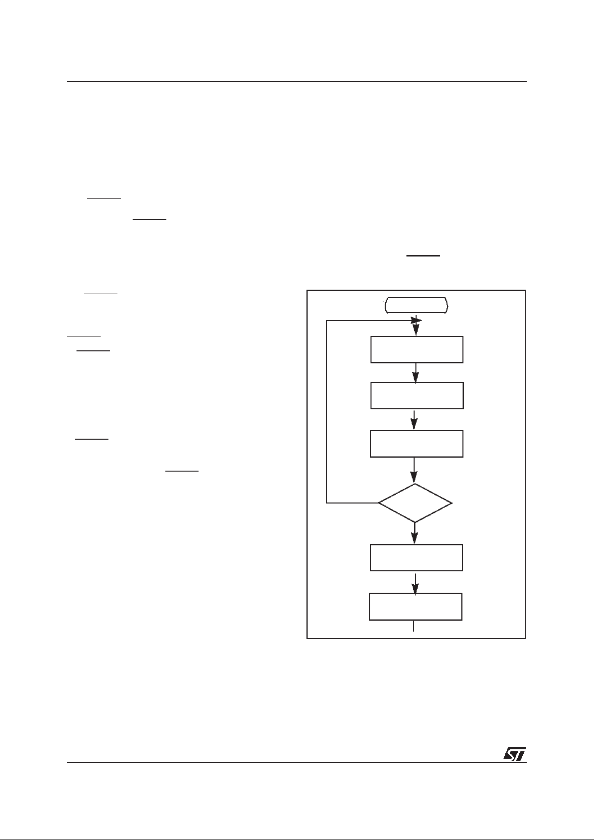
3.2.5 MCU Initialization Sequence
When a reset occurs the stack is reset, the PC is
loaded with the address of the Reset Vector (locat-
ed in program ROM starting at address 0FFEh). A
jump to the beginning of the user program must be
coded at this address. Following a Reset, the In-
terrupt flag is automatically set, so that the CPU is
in Non Maskable Interrupt mode; this prevents the
initialisation routine from being interrupted. The in-
itialisation routine should therefore be terminated
by a RETI instruction, in order to revert to normal
mode and enable interrupts. If no pending interrupt
is present at the endofthe initialisation routine, the
MCU will continue by processing the instruction
immediately following the RETIinstruction. If, how-
ever, a pending interrupt is present, it will be serv-
iced.
Figure 15.Reset and Interrupt Processing
Figure 16. Reset Block Diagram
RESET
RESET
VECTOR
JP
JP:2 BYTES/4 CYCLES
RETI
RETI: 1 BYTE/2CYCLES
INITIALIZATION
ROUTINE
VA00181
V
DD
RESET
300kΩ
2.8kΩ
POWER
WATCHDOG RESET
CK
COUNTER
RESET
ST6
INTERNAL
RESET
f
OSC
RESET
ON RESET
VA0200B
127

24/86
ST62T32B ST62E32B
RESETS (Cont’d)
Table 7. Register Reset Status
Register Address(es) Status Comment
Oscillator Control Register
EEPROM Control Register
Port Data Registers
Port Direction Register
Port Option Register
Interrupt Option Register
TIMER Status/Control
AR TIMER Status/Control 1 Register
AR TIMER Status/Control 2 Register
AR TIMER Status/Control 3 Register
AR TIMER Status/Control 4 Register
SPI Registers
0DBh
0DFh
0C0h to0C2h
0C4h to0C6h
0CCh to0CEh
0C8h
0D4h
0E8h
0E1h
0E2h
OE3h
0DCh to0DDh
00h
Main oscillator on
EEPROM enabled
I/O are Input with or without pull-up
depending on PORTPULL option
Interrupt disabled
TIMER disabled
AR TIMER stopped
SPI disabled
X, Y, V,W, Register
Accumulator
Data RAM
Data RAM Page REgister
Data ROM Window Register
EEPROM
A/D Result Register
AR TIMER Capture Register
AR TIMER Reload/Capture Register
ARTIMER Mask Registers
ARTIMER Compare Registers
080H TO083H
0FFh
084h to0BFh
0CBh
0C9h
00h to03Fh
0D0h
0DBh
0D9h
OE0h-OEFh
OEDh-OEEh
Undefined As written if programmed
TIMER Counter Register
TIMER Prescaler Register
Watchdog Counter Register
A/D Control Register
0D3h
0D2h
0D8h
0D1h
FFh
7Fh
FEh
40h
Max count loaded
A/D in Standby
UART Control
UART Data Register
OD7h
OD6h
UART disabled
128

25/86
ST62T32B ST62E32B
3.3 DIGITAL WATCHDOG
The digital Watchdog consists of a reloadable
downcounter timer which can be used to provide
controlled recovery from software upsets.
The Watchdog circuit generates a Reset when the
downcounter reaches zero. User software can
prevent this reset by reloading the counter, and
should therefore be written so that the counter is
regularly reloaded while the user program runs
correctly. In the event of a software mishap (usual-
ly caused by externally generated interference),
the user program will no longer behave in its usual
fashion and the timer register will thus not be re-
loaded periodically. Consequently the timer will
decrement down to 00h and reset the MCU. In or-
der to maximise the effectiveness of theWatchdog
function, user software must be written with this
concept in mind.
Watchdog behaviour is governed by two options,
known as “WATCHDOG ACTIVATION” (i.e.
HARDWARE or SOFTWARE) and “EXTERNAL
STOP MODE CONTROL” (seeTable 8).
In the SOFTWARE option, the Watchdog is disa-
bled until bit C of the DWDR register has been set.
When the Watchdog is disabled, low power Stop
mode is available. Once activated, the Watchdog
cannot be disabled, except by resetting the MCU.
In the HARDWARE option, the Watchdog is per-
manently enabled. Since the oscillatorwill run con-
tinuously, low power mode is not available. The
STOP instruction is interpreted as a WAIT instruc-
tion, and the Watchdog continues to countdown.
However, when the EXTERNAL STOP MODE
CONTROL option has been selected low power
consumption may be achieved in Stop Mode.
Execution of the STOP instruction is then gov-
erned by a secondary function associated with the
NMI pin. If a STOP instruction is encountered
when the NMI pin is low, it isinterpreted as WAIT,
as described above. If, however, the STOP in-
struction is encountered when the NMI pin is high,
the Watchdog counter is frozen and the CPU en-
ters STOP mode.
When theMCU exits STOP mode (i.e. when an in-
terrupt is generated), the Watchdog resumes its
activity.
Table 8. Recommended Option Choices
Functions Required Recommended Options
Stop Mode& Watchdog “EXTERNAL STOP MODE” & “HARDWARE WATCHDOG”
Stop Mode “SOFTWARE WATCHDOG”
Watchdog “HARDWARE WATCHDOG”
129

26/86
ST62T32B ST62E32B
DIGITAL WATCHDOG(Cont’d)
The Watchdog is associated with a Data space
register (Digital WatchDog Register, DWDR, loca-
tion 0D8h) which is described in greater detail in
Section 3.3.1 Digital Watchdog Register (DWDR).
This register is set to 0FEh on Reset: bit C is
cleared to “0”, which disables the Watchdog; the
timer downcounter bits, T0 to T5, and the SR bit
are allset to “1”, thus selecting the longest Watch-
dog timer period. This time period can beset to the
user’s requirements by setting the appropriate val-
ue for bits T0 to T5 in the DWDR register. The SR
bit must be set to “1”, since it is this bit which gen-
erates the Reset signal when it changes to “0”;
clearing this bit would generate an immediate Re-
set.
It should be noted that the order of the bits in the
DWDR register is inverted with respect to the as-
sociated bits in the down counter: bit 7 of the
DWDR register corresponds, in fact, to T0 and bit
2 to T5. The user should bear in mind the fact that
these bits are inverted and shifted with respect to
the physical counter bits when writing to this regis-
ter. The relationship between the DWDR register
bits and the physical implementation of the Watch-
dog timer downcounter is illustrated in Figure 17.
Only the 6 most significant bits may be used to de-
fine the time period, since it is bit 6 which triggers
the Reset when it changes to “0”. This offers the
user a choice of 64 timed periods ranging from
3,072 to 196,608 clock cycles (with an oscillator
frequency of 8MHz, this isequivalent to timer peri-
ods ranging from 384µs to 24.576ms).
Figure 17.Watchdog Counter Control
WATCHDOG CONTROL REGISTER
D0
D1
D3
D4
D5
D6
D7
WATCHDOG COUNTER
C
SR
T5
T4
T3
T2
T1
D2
T0
OSC
÷
12
RESET
VR02068A
÷
2
8
130
 Loading...