


SGS Thomson Microelectronics ST72T213G1, ST72T212G2, ST72T101G2, ST72T101G1, ST72101G2 Datasheet
...ST72101/ST72212/ST72213
8-BIT MCU WITH 4 TO 8K ROM/OTP/EPROM, 256 BYTES RAM, ADC, WDG, SPI AND 1 OR 2 TIMERS
DATASHEET
■User Program Memory (ROM/OTP/EPROM): 4 to 8K bytes
■Data RAM: 256 bytes, including 64 bytes of stack
■Master Reset and Power-On Reset
■Run, Wait, Slow, Halt and RAM Retention modes
■22 multifunctional bidirectional I/O lines:
±22 programmable interrupt inputs
±8 high sink outputs
±6 analog alternate inputs
±10 to 14 alternate functions
±EMI filtering
■Programmable watchdog (WDG)
■One or two 16-bit Timers, each featuring:
±2 Input Captures
±2 Output Compares
±External Clock input (on Timer A only)
±PWM and Pulse Generator modes
■Synchronous Serial Peripheral Interface (SPI)
■8-bit Analog-to-Digital converter (6 channels) (ST72212 and ST72213 only)
■8-bit Data Manipulation
■63 Basic Instructions
■17 main Addressing Modes
■8 x 8 Unsigned Multiply Instruction
■True Bit Manipulation
■Complete Development Support on PC/DOSWINDOWSTM Real-Time Emulator
■Full Software Package on DOS/WINDOWSTM (C-Compiler, Cross-Assembler, Debugger)
Device Summary
PSDIP32
CSDIP32W
SO28
(See ordering information at the end of datasheet)
Features |
ST72101G1 |
ST72101G2 |
ST72213G1 |
ST72212G2 |
Program Memorybytes |
4K |
8K |
4K |
8K |
RAM (stack) - bytes |
|
|
256 (64) |
|
16-bit Timers |
one |
one |
one |
two |
ADC |
no |
no |
yes |
yes |
Other Peripherals |
|
Watchdog, SPI |
|
|
Operating Supply |
|
|
3 to 5.5 V |
|
CPU Frequency |
|
8MHz max (16MHz oscillator) - 4MHz max over 85°C |
|
|
Temperature Range |
|
- 40°C to + 125°C |
|
|
Package |
|
SO28 - SDIP32 |
|
|
Rev. 1.7
September 1999 |
1/84 |

Table of Contents
1 GENERAL DESCRIPTION . . . . . . . . . . . . . . . . . . . . . . . . . . . . . . . . . . . . . . . . . . . . . . . . . . . . . . |
4 |
1.1 INTRODUCTION . . . . . . . . . . . . . . . . . . . . . . . . . . . . . . . . . . . . . . . . . . . . . . . . . . . . . . . . . 4 1.2 PIN DESCRIPTION . . . . . . . . . . . . . . . . . . . . . . . . . . . . . . . . . . . . . . . . . . . . . . . . . . . . . . . 5 1.3 EXTERNAL CONNECTIONS . . . . . . . . . . . . . . . . . . . . . . . . . . . . . . . . . . . . . . . . . . . . . . . . 9 1.4 MEMORY MAP . . . . . . . . . . . . . . . . . . . . . . . . . . . . . . . . . . . . . . . . . . . . . . . . . . . . . . . . . 10
2 CENTRAL PROCESSING UNIT . . . . . . . . . . . . . . . . . . . . . . . . . . . . . . . . . . . . . . . . . . . . . . . . . |
13 |
|
2.1 |
INTRODUCTION . . . . . . . . . . . . . . . . . . . . . . . . . . . . . . . . . . . . . . . . . . . . . . . . . . . . . . . . |
13 |
2.2 |
MAIN FEATURES . . . . . . . . . . . . . . . . . . . . . . . . . . . . . . . . . . . . . . . . . . . . . . . . . . . . . . . |
13 |
2.3 |
CPU REGISTERS . . . . . . . . . . . . . . . . . . . . . . . . . . . . . . . . . . . . . . . . . . . . . . . . . . . . . . . |
13 |
3 CLOCKS, RESET, INTERRUPTS & POWER SAVING MODES . . . . . . . . . . . . . . . . . . . . . . . . |
16 |
|
3.1 CLOCK SYSTEM . . . . . . . . . . . . . . . . . . . . . . . . . . . . . . . . . . . . . . . . . . . . . . . . . . . . . . . . 16
3.1.1 General Description . . . . . . . . . . . . . . . . . . . . . . . . . . . . . . . . . . . . . . . . . . . . . . . . . 16
3.2 RESET . . . . . . . . . . . . . . . . . . . . . . . . . . . . . . . . . . . . . . . . . . . . . . . . . . . . . . . . . . . . . . . . 17
3.2.1 Introduction . . . . . . . . . . . . . . . . . . . . . . . . . . . . . . . . . . . . . . . . . . . . . . . . . . . . . . . 17
3.2.2 External Reset . . . . . . . . . . . . . . . . . . . . . . . . . . . . . . . . . . . . . . . . . . . . . . . . . . . . . 17
3.2.3 Reset Operation . . . . . . . . . . . . . . . . . . . . . . . . . . . . . . . . . . . . . . . . . . . . . . . . . . . . 17
3.2.4 Power-on Reset . . . . . . . . . . . . . . . . . . . . . . . . . . . . . . . . . . . . . . . . . . . . . . . . . . . . 17
3.3 INTERRUPTS . . . . . . . . . . . . . . . . . . . . . . . . . . . . . . . . . . . . . . . . . . . . . . . . . . . . . . . . . . 18
3.4 POWER SAVING MODES . . . . . . . . . . . . . . . . . . . . . . . . . . . . . . . . . . . . . . . . . . . . . . . . . 21
3.4.1 Introduction . . . . . . . . . . . . . . . . . . . . . . . . . . . . . . . . . . . . . . . . . . . . . . . . . . . . . . . 21
3.4.2 Slow Mode . . . . . . . . . . . . . . . . . . . . . . . . . . . . . . . . . . . . . . . . . . . . . . . . . . . . . . . . 21
3.4.3 Wait Mode . . . . . . . . . . . . . . . . . . . . . . . . . . . . . . . . . . . . . . . . . . . . . . . . . . . . . . . . 21
3.4.4 Halt Mode . . . . . . . . . . . . . . . . . . . . . . . . . . . . . . . . . . . . . . . . . . . . . . . . . . . . . . . . . 22
3.5 MISCELLANEOUS REGISTER . . . . . . . . . . . . . . . . . . . . . . . . . . . . . . . . . . . . . . . . . . . . . 23
4 ON-CHIP PERIPHERALS . . . . . . . . . . . . . . . . . . . . . . . . . . . . . . . . . . . . . . . . . . . . . . . . . . . . . . 24
4.1 I/O PORTS . . . . . . . . . . . . . . . . . . . . . . . . . . . . . . . . . . . . . . . . . . . . . . . . . . . . . . . . . . . . . 24
4.1.1 Introduction . . . . . . . . . . . . . . . . . . . . . . . . . . . . . . . . . . . . . . . . . . . . . . . . . . . . . . . 24
4.1.2 Functional Description . . . . . . . . . . . . . . . . . . . . . . . . . . . . . . . . . . . . . . . . . . . . . . . 24
4.1.3 I/O Port Implementation . . . . . . . . . . . . . . . . . . . . . . . . . . . . . . . . . . . . . . . . . . . . . . 25
4.1.4 Register Description . . . . . . . . . . . . . . . . . . . . . . . . . . . . . . . . . . . . . . . . . . . . . . . . . 28
4.2 WATCHDOG TIMER (WDG) . . . . . . . . . . . . . . . . . . . . . . . . . . . . . . . . . . . . . . . . . . . . . . . 30
4.2.1 Introduction . . . . . . . . . . . . . . . . . . . . . . . . . . . . . . . . . . . . . . . . . . . . . . . . . . . . . . . 30
4.2.2 Main Features . . . . . . . . . . . . . . . . . . . . . . . . . . . . . . . . . . . . . . . . . . . . . . . . . . . . . 30
4.2.3 Functional Description . . . . . . . . . . . . . . . . . . . . . . . . . . . . . . . . . . . . . . . . . . . . . . . 31
4.2.4 Low Power Modes . . . . . . . . . . . . . . . . . . . . . . . . . . . . . . . . . . . . . . . . . . . . . . . . . . 31
4.2.5 Interrupts . . . . . . . . . . . . . . . . . . . . . . . . . . . . . . . . . . . . . . . . . . . . . . . . . . . . . . . . . 31
4.2.6 Register Description . . . . . . . . . . . . . . . . . . . . . . . . . . . . . . . . . . . . . . . . . . . . . . . . . 31
4.3 16-BIT TIMER . . . . . . . . . . . . . . . . . . . . . . . . . . . . . . . . . . . . . . . . . . . . . . . . . . . . . . . . . . 32
4.3.1 Introduction . . . . . . . . . . . . . . . . . . . . . . . . . . . . . . . . . . . . . . . . . . . . . . . . . . . . . . . 32
4.3.2 Main Features . . . . . . . . . . . . . . . . . . . . . . . . . . . . . . . . . . . . . . . . . . . . . . . . . . . . . 32
4.3.3 Functional Description . . . . . . . . . . . . . . . . . . . . . . . . . . . . . . . . . . . . . . . . . . . . . . . 32
4.3.4 Low Power Modes . . . . . . . . . . . . . . . . . . . . . . . . . . . . . . . . . . . . . . . . . . . . . . . . . 43
4.3.5 Interrupts . . . . . . . . . . . . . . . . . . . . . . . . . . . . . . . . . . . . . . . . . . . . . . . . . . . . . . . . . 43
4.3.6 Register Description . . . . . . . . . . . . . . . . . . . . . . . . . . . . . . . . . . . . . . . . . . . . . 95. . . . 44
2/84

Table of Contents
4.4 SERIAL PERIPHERAL INTERFACE (SPI) . . . . . . . . . . . . . . . . . . . . . . . . . . . . . . . . . . . . |
49 |
4.4.1 Introduction . . . . . . . . . . . . . . . . . . . . . . . . . . . . . . . . . . . . . . . . . . . . . . . . . . . . . . . 49 4.4.2 Main Features . . . . . . . . . . . . . . . . . . . . . . . . . . . . . . . . . . . . . . . . . . . . . . . . . . . . . 49 4.4.3 General description . . . . . . . . . . . . . . . . . . . . . . . . . . . . . . . . . . . . . . . . . . . . . . . . . 49 4.4.4 Functional Description . . . . . . . . . . . . . . . . . . . . . . . . . . . . . . . . . . . . . . . . . . . . . . . 51 4.4.5 Low Power Modes . . . . . . . . . . . . . . . . . . . . . . . . . . . . . . . . . . . . . . . . . . . . . . . . . . 58 4.4.6 Interrupts . . . . . . . . . . . . . . . . . . . . . . . . . . . . . . . . . . . . . . . . . . . . . . . . . . . . . . . . . 58 4.4.7 Register Description . . . . . . . . . . . . . . . . . . . . . . . . . . . . . . . . . . . . . . . . . . . . . . . . . 59
4.5 8-BIT A/D CONVERTER (ADC) . . . . . . . . . . . . . . . . . . . . . . . . . . . . . . . . . . . . . . . . . . . . . 62
4.5.1 Introduction . . . . . . . . . . . . . . . . . . . . . . . . . . . . . . . . . . . . . . . . . . . . . . . . . . . . . . . 62
4.5.2 Main Features . . . . . . . . . . . . . . . . . . . . . . . . . . . . . . . . . . . . . . . . . . . . . . . . . . . . . 62
4.5.3 Functional Description . . . . . . . . . . . . . . . . . . . . . . . . . . . . . . . . . . . . . . . . . . . . . . . 63
4.5.4 Low Power Modes . . . . . . . . . . . . . . . . . . . . . . . . . . . . . . . . . . . . . . . . . . . . . . . . . . 63
4.5.5 Interrupts . . . . . . . . . . . . . . . . . . . . . . . . . . . . . . . . . . . . . . . . . . . . . . . . . . . . . . . . . 63
4.5.6 Register Description . . . . . . . . . . . . . . . . . . . . . . . . . . . . . . . . . . . . . . . . . . . . . . . . . 64
5 INSTRUCTION SET . . . . . . . . . . . . . . . . . . . . . . . . . . . . . . . . . . . . . . . . . . . . . . . . . . . . . . . . . . |
65 |
5.1 ST7 ADDRESSING MODES . . . . . . . . . . . . . . . . . . . . . . . . . . . . . . . . . . . . . . . . . . . . . . . |
65 |
5.1.1 Inherent . . . . . . . . . . . . . . . . . . . . . . . . . . . . . . . . . . . . . . . . . . . . . . . . . . . . . . . . . . 66 5.1.2 Immediate . . . . . . . . . . . . . . . . . . . . . . . . . . . . . . . . . . . . . . . . . . . . . . . . . . . . . . . . 66 5.1.3 Direct . . . . . . . . . . . . . . . . . . . . . . . . . . . . . . . . . . . . . . . . . . . . . . . . . . . . . . . . . . . . 66 5.1.4 Indexed (No Offset, Short, Long) . . . . . . . . . . . . . . . . . . . . . . . . . . . . . . . . . . . . . . . 66 5.1.5 Indirect (Short, Long) . . . . . . . . . . . . . . . . . . . . . . . . . . . . . . . . . . . . . . . . . . . . . . . . 66 5.1.6 Indirect Indexed (Short, Long) . . . . . . . . . . . . . . . . . . . . . . . . . . . . . . . . . . . . . . . . . 67 5.1.7 Relative mode (Direct, Indirect) . . . . . . . . . . . . . . . . . . . . . . . . . . . . . . . . . . . . . . . . 67
5.2 INSTRUCTION GROUPS . . . . . . . . . . . . . . . . . . . . . . . . . . . . . . . . . . . . . . . . . . . . . . . . . 68
6 ELECTRICAL CHARACTERISTICS . . . . . . . . . . . . . . . . . . . . . . . . . . . . . . . . . . . . . . . . . . . . . . 71
6.1 ABSOLUTE MAXIMUM RATINGS . . . . . . . . . . . . . . . . . . . . . . . . . . . . . . . . . . . . . . . . . . . 71 6.2 RECOMMENDED OPERATING CONDITIONS . . . . . . . . . . . . . . . . . . . . . . . . . . . . . . . . . 72 6.3 DC ELECTRICAL CHARACTERISTICS . . . . . . . . . . . . . . . . . . . . . . . . . . . . . . . . . . . . . . 73 6.4 RESET CHARACTERISTICS . . . . . . . . . . . . . . . . . . . . . . . . . . . . . . . . . . . . . . . . . . . . . . 74 6.5 OSCILLATOR CHARACTERISTICS . . . . . . . . . . . . . . . . . . . . . . . . . . . . . . . . . . . . . . . . . 74 6.6 A/D CONVERTER CHARACTERISTICS (ST72212 AND ST72213 ONLY) . . . . . . . . . . . 75 6.7 SPI CHARACTERISTICS . . . . . . . . . . . . . . . . . . . . . . . . . . . . . . . . . . . . . . . . . . . . . . . . . 77
7 GENERAL INFORMATION . . . . . . . . . . . . . . . . . . . . . . . . . . . . . . . . . . . . . . . . . . . . . . . . . . . . . 80
7.1 EPROM ERASURE . . . . . . . . . . . . . . . . . . . . . . . . . . . . . . . . . . . . . . . . . . . . . . . . . . . . . . 80 7.2 PACKAGE MECHANICAL DATA . . . . . . . . . . . . . . . . . . . . . . . . . . . . . . . . . . . . . . . . . . . . 80 7.3 ORDERING INFORMATION . . . . . . . . . . . . . . . . . . . . . . . . . . . . . . . . . . . . . . . . . . . . . . . 82
7.3.1 Transfer Of Customer Code . . . . . . . . . . . . . . . . . . . . . . . . . . . . . . . . . . . . . . . . . . . 82
8 SUMMARY OF CHANGES . . . . . . . . . . . . . . . . . . . . . . . . . . . . . . . . . . . . . . . . . . . . . . . . . . . . . 84
3/84
ST72101/ST72212/ST72213
1 GENERAL DESCRIPTION
1.1 INTRODUCTION
The ST72101, ST72213 and ST72212 HCMOS Microcontroller Units are members of the ST7 family. These devices are based on an industrystandard 8-bit core and feature an enhanced instruction set. They normally operate at a 16MHz oscillator frequency. Under software control, the ST72101, ST72213 and ST72212 may be placed in either WAIT, SLOW or HALT modes, thus reducing power consumption. The enhanced instruction set and addressing modes afford real programming potential. In addition to standard 8-bit data management, the ST72101, ST72213 and ST72212 feature true bit manipulation, 8x8
unsigned multiplication and indirect addressing modes on the whole memory. The devices include an on-chip oscillator, CPU, program memory (ROM/OTP/EPROM versions), RAM, 22 I/O lines and the following on-chip peripherals: Analog-to- Digital Converter (ADC) with 6 multiplexed analog inputs (ST72212 and ST72213 only), industry standard synchronous SPI serial interface, digital Watchdog, one or two independent 16-bit Timers, one featuring an External Clock Input, and both featuring Pulse Generator capabilities, 2 Input Captures and 2 Output Compares.
Figure 1. ST72101, ST72213 and ST72212 Block Diagram
|
Internal |
OSCIN |
CLOCK |
OSCOUT |
OSC |
|
|
RESET |
CONTROL |
|
8-BIT CORE |
|
ALU |
|
PROGRAM |
|
MEMORY |
|
(4 - 8K Bytes) |
|
RAM |
|
(256 Bytes) |
VDD |
POWER |
|
|
VSS |
SUPPLY |
|
BUS DATA AND ADDRESS
PORT A |
PA0 -> PA7 |
|
|
(8 bits) |
|
SPI |
|
|
PORT B |
PB0 -> PB7 |
|
|
(8 bits) |
|
TIMER A |
|
|
PORT C |
PC0 -> PC5 |
|
(6 bits) |
||
|
||
8-BIT ADC 1) |
|
|
TIMER B2) |
|
|
WATCHDOG |
|
1)ST72213 and ST72212 only
2)ST72212 only
4/84
1.2 PIN DESCRIPTION
Figure 2. ST72212 Pinout (SO28)
RESET |
1 |
28 |
VDD |
OSCIN |
2 |
27 |
VSS |
OSCOUT |
3 |
26 |
1) |
TEST/VPP |
|||
SS/PB7 |
4 |
25 |
PA0 |
SCK/PB6 |
5 |
24 |
PA1 |
MISO/PB5 |
6 |
23 |
PA2 |
MOSI/PB4 |
7 |
22 |
PA3 |
OCMP2_A/PB3 |
8 |
21 |
PA4 |
ICAP2_A/PB2 |
9 |
20 |
PA5 |
OCMP1_A/PB1 |
10 |
19 |
PA6 |
ICAP1_A/PB0 |
11 |
18 |
PA7 |
AIN5/EXTCLK_A/PC5 |
12 |
17 |
PC0/ICAP1_B/AIN0 |
AIN4/OCMP2_B/PC4 |
13 |
16 |
PC1/OCMP1_B/AIN1 |
AIN3/ICAP2_B/PC3 |
14 |
15 |
PC2/CLKOUT/AIN2 |
1)V on EPROM/OTP only PP
Figure 3. ST72213 Pinout (SO28)
RESET |
1 |
28 |
VDD |
OSCIN |
2 |
27 |
VSS |
OSCOUT |
3 |
26 |
1) |
TEST/V PP |
|||
SS/PB7 |
4 |
25 |
PA0 |
SCK/PB6 |
5 |
24 |
PA1 |
MISO/PB5 |
6 |
23 |
PA2 |
MOSI/PB4 |
7 |
22 |
PA3 |
OCMP2_A/PB3 |
8 |
21 |
PA4 |
ICAP2_A/PB2 |
9 |
20 |
PA5 |
OCMP1_A/PB1 |
10 |
19 |
PA6 |
ICAP1_A/PB0 |
11 |
18 |
PA7 |
AIN5/EXTCLK_A/PC5 |
12 |
17 |
PC0/AIN0 |
AIN4/PC4 |
13 |
16 |
PC1/AIN1 |
AIN3/PC3 |
14 |
15 |
PC2/CLKOUT/AIN2 |
1)V on EPROM/OTP only PP
Figure 4. ST72101 Pinout (SO28)
RESET |
1 |
28 |
VDD |
OSCIN |
2 |
27 |
VSS |
OSCOUT |
3 |
26 |
1) |
TEST/V PP |
|||
SS/PB7 |
4 |
25 |
PA0 |
SCK/PB6 |
5 |
24 |
PA1 |
MISO/PB5 |
6 |
23 |
PA2 |
MOSI/PB4 |
7 |
22 |
PA3 |
OCMP2_A/PB3 |
8 |
21 |
PA4 |
ICAP2_A/PB2 |
9 |
20 |
PA5 |
OCMP1_A/PB1 |
10 |
19 |
PA6 |
ICAP1_A/PB0 |
11 |
18 |
PA7 |
EXTCLK_A/PC5 |
12 |
17 |
PC0 |
PC4 |
13 |
16 |
PC1 |
PC3 |
14 |
15 |
PC2/CLKOUT |
1)V on EPROM/OTP only PP
ST72101/ST72212/ST72213
Figure 5. ST72212 Pinout (SDIP32)
RESET |
1 |
32 |
VDD |
OSCIN |
2 |
31 |
VSS |
OSCOUT |
3 |
30 |
1) |
TEST/VPP |
|||
SS/PB7 |
4 |
29 |
PA0 |
SCK/PB6 |
5 |
28 |
PA1 |
MISO/PB5 |
6 |
27 |
PA2 |
MOSI/PB4 |
7 |
26 |
PA3 |
NC |
8 |
25 |
NC |
NC |
9 |
24 |
NC |
OCMP2_A/PB3 |
10 |
23 |
PA4 |
ICAP2_A/PB2 |
11 |
22 |
PA5 |
OCMP1_A/PB1 |
12 |
21 |
PA6 |
ICAP1_A/PB0 |
13 |
20 |
PA7 |
AIN5/EXTCLK_A/PC5 |
14 |
19 |
PC0/ICAP1_B/AIN0 |
AIN4/OCMP2_B/PC4 |
15 |
18 |
PC1/OCMP1_B/AIN1 |
AIN3/ICAP2_B/PC3 |
16 |
17 |
PC2/CLKOUT/AIN2 |
1)V on EPROM/OTP only PP
Figure 6. ST72213 Pinout (SDIP32)
RESET |
1 |
32 |
VDD |
OSCIN |
2 |
31 |
VSS |
OSCOUT |
3 |
30 |
1) |
TEST/V PP |
|||
SS/PB7 |
4 |
29 |
PA0 |
SCK/PB6 |
5 |
28 |
PA1 |
MISO/PB5 |
6 |
27 |
PA2 |
MOSI/PB4 |
7 |
26 |
PA3 |
NC |
8 |
25 |
NC |
NC |
9 |
24 |
NC |
OCMP2_A/PB3 |
10 |
23 |
PA4 |
ICAP2_A/PB2 |
11 |
22 |
PA5 |
OCMP1_A/PB1 |
12 |
21 |
PA6 |
ICAP1_A/PB0 |
13 |
20 |
PA7 |
AIN5/EXTCLK_A/PC5 |
14 |
19 |
PC0/AIN0 |
AIN4/PC4 |
15 |
18 |
PC1/AIN1 |
AIN3/PC3 |
16 |
17 |
PC2/CLKOUT/AIN2 |
1)V on EPROM/OTP only PP
Figure 7. ST72101 Pinout (SDIP32)
RESET |
1 |
32 |
VDD |
OSCIN |
2 |
31 |
VSS |
OSCOUT |
3 |
30 |
1) |
TEST/V PP |
|||
SS/PB7 |
4 |
29 |
PA0 |
SCK/PB6 |
5 |
28 |
PA1 |
MISO/PB5 |
6 |
27 |
PA2 |
MOSI/PB4 |
7 |
26 |
PA3 |
NC |
8 |
25 |
NC |
NC |
9 |
24 |
NC |
OCMP2_A/PB3 |
10 |
23 |
PA4 |
ICAP2_A/PB2 |
11 |
22 |
PA5 |
OCMP1_A/PB1 |
12 |
21 |
PA6 |
ICAP1_A/PB0 |
13 |
20 |
PA7 |
EXTCLK_A/PC5 |
14 |
19 |
PC0 |
PC4 |
15 |
18 |
PC1 |
PC3 |
16 |
17 |
PC2/CLKOUT |
1)V on EPROM/OTP only PP
5/84

ST72101/ST72212/ST72213
Table 1. ST72212 Pin Configuration
Pin n° |
Pin n ° |
Pin Name |
Type |
Descriptio n |
Remarks |
|
SDIP32 |
SO28 |
|||||
|
|
|
|
|||
1 |
1 |
RESET |
I/O |
Bidirectional. Active low. Top priority non maskable interrupt. |
||
2 |
2 |
OSCIN |
I |
Input/Output Oscillator pin. These pins connect a parallel-resonant |
||
|
|
|
|
|||
3 |
3 |
OSCOUT |
O |
crystal, or an external source to the on-chip oscillator. |
||
|
|
|||||
4 |
4 |
PB7/SS |
I/O |
Port B7 or SPI Slave Select (active low) |
External Interrupt: EI1 |
|
5 |
5 |
PB6/SCK |
I/O |
Port B6 or SPI Serial Clock |
External Interrupt: EI1 |
|
6 |
6 |
PB5/MISO |
I/O |
Port B5 or SPI Master In/ Slave Out Data |
External Interrupt: EI1 |
|
7 |
7 |
PB4/MOSI |
I/O |
Port B4 or SPI Master Out / Slave In Data |
External Interrupt: EI1 |
|
8 |
|
NC |
|
Not Connected |
|
|
9 |
|
NC |
|
Not Connected |
|
|
10 |
8 |
PB3/OCMP2_A |
I/O |
Port B3 or TimerA Output Compare 2 |
External Interrupt: EI1 |
|
11 |
9 |
PB2/ICAP2_A |
I/O |
Port B2 or TimerA Input Capture 2 |
External Interrupt: EI1 |
|
12 |
10 |
PB1/OCMP1_A |
I/O |
Port B1 or TimerA Output Compare 1 |
External Interrupt: EI1 |
|
13 |
11 |
PB0/ICAP1_A |
I/O |
Port B0 or TimerA Input Capture 1 |
External Interrupt: EI1 |
|
14 |
12 |
PC5/EXTCLK_A/AIN5 |
I/O |
Port C5 or TimerA Input Clock or ADCAnalog Input 5 External Interrupt: EI1 |
||
15 |
13 |
PC4/OCMP2_B/AIN4 |
I/O |
Port C4orTimerB Output Compare 2or ADCAnalog |
External Interrupt: EI1 |
|
|
|
|
|
Input 4 |
|
|
16 |
14 |
PC3/ICAP2_B/AIN3 |
I/O |
Port C3 or TimerB Input Capture 2 or ADC Analog |
External Interrupt: EI1 |
|
|
|
|
|
Input 3 |
|
|
|
|
|
|
Port C2or Internal Clock Frequency Output or ADC |
|
|
17 |
15 |
PC2/CLKOUT/AIN2 |
I/O |
Analog Input 2. Clockout is driven by Bit 5 of the |
External Interrupt: EI1 |
|
|
|
|
|
miscellaneous register. |
|
|
18 |
16 |
PC1/OCMP1_B/AIN1 |
I/O |
Port C1orTimerB Output Compare 1or ADCAnalog |
External Interrupt: EI1 |
|
|
|
|
|
Input 1 |
|
|
19 |
17 |
PC0/ICAP1_B/AIN0 |
I/O |
Port C0 or TimerB Input Capture 1 or ADC Analog |
External Interrupt: EI1 |
|
|
|
|
|
Input 0 |
|
|
20 |
18 |
PA7 |
I/O |
Port A7, High Sink |
External Interrupt: EI0 |
|
21 |
19 |
PA6 |
I/O |
Port A6, High Sink |
External Interrupt: EI0 |
|
22 |
20 |
PA5 |
I/O |
Port A5, High Sink |
External Interrupt: EI0 |
|
23 |
21 |
PA4 |
I/O |
Port A4, High Sink |
External Interrupt: EI0 |
|
24 |
|
NC |
|
Not Connected |
|
|
25 |
|
NC |
|
Not Connected |
|
|
26 |
22 |
PA3 |
I/O |
Port A3, High Sink |
External Interrupt: EI0 |
|
27 |
23 |
PA2 |
I/O |
Port A2, High Sink |
External Interrupt: EI0 |
|
28 |
24 |
PA1 |
I/O |
Port A1, High Sink |
External Interrupt: EI0 |
|
29 |
25 |
PA0 |
I/O |
Port A0, High Sink |
External Interrupt: EI0 |
|
30 |
26 |
(1) |
I/S |
Test mode pin (should be tied low in user mode). In the EPROM program- |
||
TEST/VPP |
ming mode, this pin acts as the programming voltage input VPP. |
|||||
|
|
|
|
|||
31 |
27 |
VSS |
S |
Ground |
|
|
32 |
28 |
VDD |
S |
Main power supply |
|
|
Note 1: VPP on EPROM/OTP only |
|
|
|
|||
6/84
|
|
|
|
ST72101/ST72212/ST72213 |
||
Table 2. ST72213 Pin Configuration |
|
|
||||
Pin n° |
Pin n° |
Pin Name |
Type |
Description |
Remarks |
|
SDIP32 |
SO28 |
|||||
|
|
|
|
|||
1 |
1 |
RESET |
I/O |
Bidirectional. Active low. Top priority non maskable interrup t. |
||
2 |
2 |
OSCIN |
I |
Input/Output Oscillator pin. These pins connect a parallel-resonant |
||
|
|
|
|
|||
3 |
3 |
OSCOUT |
O |
crystal, or an external source to the on-chip oscillator. |
||
|
|
|||||
4 |
4 |
PB7/SS |
I/O |
Port B7 or SPI Slave Select (active low) |
External Interrupt: EI1 |
|
5 |
5 |
PB6/SCK |
I/O |
Port B6 or SPI Serial Clock |
External Interrupt: EI1 |
|
6 |
6 |
PB5/MISO |
I/O |
Port B5 or SPI Master In/ Slave Out Data |
External Interrupt: EI1 |
|
7 |
7 |
PB4/MOSI |
I/O |
Port B4 or SPI Master Out / Slave In Data |
External Interrupt: EI1 |
|
8 |
|
NC |
|
Not Connected |
|
|
9 |
|
NC |
|
Not Connected |
|
|
10 |
8 |
PB3/OCMP2_A |
I/O |
Port B3 or TimerA Output Compare 2 |
External Interrupt: EI1 |
|
11 |
9 |
PB2/ICAP2_A |
I/O |
Port B2 or TimerA Input Capture 2 |
External Interrupt: EI1 |
|
12 |
10 |
PB1/OCMP1_A |
I/O |
Port B1 or TimerA Output Compare 1 |
External Interrupt: EI1 |
|
13 |
11 |
PB0/ICAP1_A |
I/O |
Port B0 or TimerA Input Capture 1 |
External Interrupt: EI1 |
|
14 |
12 |
PC5/EXTCLK_A/AIN5 |
I/O |
Port C5 or TimerA Input Clock or ADC Analog |
External Interrupt: EI1 |
|
Input 5 |
||||||
|
|
|
|
|
||
15 |
13 |
PC4/AIN4 |
I/O |
Port C4 or ADC Analog Input 4 |
External Interrupt: EI1 |
|
16 |
14 |
PC3/AIN3 |
I/O |
Port C3 or ADC Analog Input 3 |
External Interrupt: EI1 |
|
|
|
|
|
Port C2 or Internal Clock Frequency Output or |
|
|
17 |
15 |
PC2/CLKOUT/AIN2 |
I/O |
ADC Analog Input 2. Clockout is driven by Bit 5 |
External Interrupt: EI1 |
|
|
|
|
|
of the miscellaneous register. |
|
|
18 |
16 |
PC1/AIN1 |
I/O |
Port C1 or ADC Analog Input 1 |
External Interrupt: EI1 |
|
19 |
17 |
PC0/AIN0 |
I/O |
Port C0 or ADC Analog Input 0 |
External Interrupt: EI1 |
|
20 |
18 |
PA7 |
I/O |
Port A7, High Sink |
External Interrupt: EI0 |
|
21 |
19 |
PA6 |
I/O |
Port A6, High Sink |
External Interrupt: EI0 |
|
22 |
20 |
PA5 |
I/O |
Port A5, High Sink |
External Interrupt: EI0 |
|
23 |
21 |
PA4 |
I/O |
Port A4, High Sink |
External Interrupt: EI0 |
|
24 |
|
NC |
|
Not Connected |
|
|
25 |
|
NC |
|
Not Connected |
|
|
26 |
22 |
PA3 |
I/O |
Port A3, High Sink |
External Interrupt: EI0 |
|
27 |
23 |
PA2 |
I/O |
Port A2, High Sink |
External Interrupt: EI0 |
|
28 |
24 |
PA1 |
I/O |
Port A1, High Sink |
External Interrupt: EI0 |
|
29 |
25 |
PA0 |
I/O |
Port A0, High Sink |
External Interrupt: EI0 |
|
30 |
26 |
(1) |
I/S |
Test mode pin (should be tied low in user mode). In the EPROM pro- |
||
TEST/VPP |
gramming mode, this pin acts as the programming voltage input VPP. |
|||||
|
|
|
|
|||
31 |
27 |
VSS |
S |
Ground |
|
|
32 |
28 |
VDD |
S |
Main power supply |
|
|
Note 1: VPP on EPROM/OTP only |
|
|
|
|||
7/84
ST72101/ST72212/ST72213
Table 3. ST72101 Pin Configuration
Pin n° |
Pin n° |
Pin Name |
Type |
Description |
Remarks |
|
SDIP32 |
SO28 |
|||||
|
|
|
|
|||
1 |
1 |
RESET |
I/O |
Bidirectional. Active low. Top priority non maskable interrupt. |
||
2 |
2 |
OSCIN |
I |
Input/Output Oscillator pin. These pins connect a parallel-resonant crystal, or |
||
|
|
|
|
|||
3 |
3 |
OSCOUT |
O |
an external source to the on-chip oscillator. |
|
|
|
|
|||||
4 |
4 |
PB7/SS |
I/O |
Port B7 or SPI Slave Select (active low) |
External Interrupt: EI1 |
|
5 |
5 |
PB6/SCK |
I/O |
Port B6 or SPI Serial Clock |
External Interrupt: EI1 |
|
6 |
6 |
PB5/MISO |
I/O |
Port B5 or SPI Master In/ Slave Out Data |
External Interrupt: EI1 |
|
7 |
7 |
PB4/MOSI |
I/O |
Port B4 or SPI Master Out / Slave In Data |
External Interrupt: EI1 |
|
8 |
|
NC |
|
Not Connected |
|
|
9 |
|
NC |
|
Not Connected |
|
|
10 |
8 |
PB3/OCMP2_A |
I/O |
Port B3 or TimerA Output Compare 2 |
External Interrupt: EI1 |
|
11 |
9 |
PB2/ICAP2_A |
I/O |
Port B2 or TimerA Input Capture 2 |
External Interrupt: EI1 |
|
12 |
10 |
PB1/OCMP1_A |
I/O |
Port B1 or TimerA Output Compare 1 |
External Interrupt: EI1 |
|
13 |
11 |
PB0/ICAP1_A |
I/O |
Port B0 or TimerA Input Capture 1 |
External Interrupt: EI1 |
|
14 |
12 |
PC5/EXTCLK_A |
I/O |
Port C5 or TimerA Input Clock |
External Interrupt: EI1 |
|
15 |
13 |
PC4 |
I/O |
Port C4 |
External Interrupt: EI1 |
|
16 |
14 |
PC3 |
I/O |
Port C3 |
External Interrupt: EI1 |
|
17 |
15 |
PC2/CLKOUT |
I/O |
Port C2 or Internal Clock Frequency Output. Clockout |
External Interrupt: EI1 |
|
|
|
|
|
is driven by MCO bit of the miscellaneous register. |
|
|
18 |
16 |
PC1 |
I/O |
Port C1 |
External Interrupt: EI1 |
|
19 |
17 |
PC0 |
I/O |
Port C0 |
External Interrupt: EI1 |
|
20 |
18 |
PA7 |
I/O |
Port A7, High Sink |
External Interrupt: EI0 |
|
21 |
19 |
PA6 |
I/O |
Port A6, High Sink |
External Interrupt: EI0 |
|
22 |
20 |
PA5 |
I/O |
Port A5, High Sink |
External Interrupt: EI0 |
|
23 |
21 |
PA4 |
I/O |
Port A4, High Sink |
External Interrupt: EI0 |
|
24 |
|
NC |
|
Not Connected |
|
|
25 |
|
NC |
|
Not Connected |
|
|
26 |
22 |
PA3 |
I/O |
Port A3, High Sink |
External Interrupt: EI0 |
|
27 |
23 |
PA2 |
I/O |
Port A2, High Sink |
External Interrupt: EI0 |
|
28 |
24 |
PA1 |
I/O |
Port A1, High Sink |
External Interrupt: EI0 |
|
29 |
25 |
PA0 |
I/O |
Port A0, High Sink |
External Interrupt: EI0 |
|
30 |
26 |
(1) |
I/S |
Test mode pin (should be tied low in user mode). In the EPROM programming |
||
TEST/VPP |
mode, this pin acts as the programming voltage input VPP. |
|||||
|
|
|
|
|||
31 |
27 |
VSS |
S |
Ground |
|
|
32 |
28 |
VDD |
S |
Main power supply |
|
|
Note 1: VPP on EPROM/OTP only. |
|
|
|
|||
8/84
ST72101/ST72212/ST72213
1.3 EXTERNAL CONNECTIONS
The following figure shows the recommended external connections for the device.
The VPP pin is only used for programming OTP and EPROM devices and must be tied to ground in user mode.
The 10 nF and 0.1 μF decoupling capacitors on the power supply lines are a suggested EMC performance/cost tradeoff.
Figure 8. Recommended External Connections
The external reset network is intended to protect the device against parasitic resets, especially in noisy environments.
Unused I/Os should be tied high to avoid any unnecessary power consumption on floating lines. An alternative solution is to program the unused ports as inputs with pull-up.
|
|
VPP |
|
VDD |
+ |
VDD |
|
10nF |
0.1μF |
||
|
|||
|
|
VSS |
|
VDD |
|
4.7K |
|
0.1μF |
EXTERNAL RESET CIRCUIT |
RESET |
|
0.1μF |
See OSCIN
Clocks
Section OSCOUT
Or configure unused I/O ports by software as input with pull-up
VDD |
10K |
Unused I/O |
9/84
ST72101/ST72212/ST72213
1.4 MEMORY MAP
Figure 9. Memory Map
0000h |
|
HW Registers |
0080h |
(see Table 5) |
Short Addressing |
007Fh |
RAM (zero page) |
0080h |
00FFh |
|
|
|
0100h |
|
16-bit Addressing |
256 Bytes RAM |
RAM |
|
|
|
013Fh |
017Fh |
0140h |
0180h |
64 Bytes Stack or |
|
16-bit Addressing RAM |
Reserved |
017Fh |
DFFFh
E000h
8K Bytes
Program Memory
F000h
4K Bytes
Program
Memory
FFDFh
FFE0h
Interrupt & Reset Vectors
(see Table 4)
FFFFh
Table 4. Interrupt Vector Map
Vector Address |
Description |
Remarks |
FFE0-FFE1h |
Not Used |
|
FFE2-FFE3h |
Not Used |
|
FFE4-FFE5h |
Not Used |
|
FFE6-FFE7h |
Not Used |
|
FFE8-FFE9h |
Not Used |
|
FFEA-FFEBh |
Not Used |
|
FFEC-FFEDh |
Not Used |
|
FFEE-FFEFh |
TIMER B Interrupt Vector (ST72212 only) |
Internal Interrupt |
FFF0-FFF1h |
Not Used |
|
FFF2-FFF3h |
TIMER A Interrupt Vector |
Internal Interrupt |
FFF4-FFF5h |
SPI Interrupt Vector |
Internal Interrupt |
FFF6-FFF7h |
Not Used |
|
FFF8-FFF9h |
External Interrupt Vector EI1 |
External Interrupt |
FFFA-FF FBh |
External Interrupt Vector EI0 |
External Interrupt |
FFFC-FFFDh |
TRAP (software) Interrupt Vector |
CPU Interrupt |
FFFE-FFFFh |
RESET Vector |
|
10/84
ST72101/ST72212/ST72213
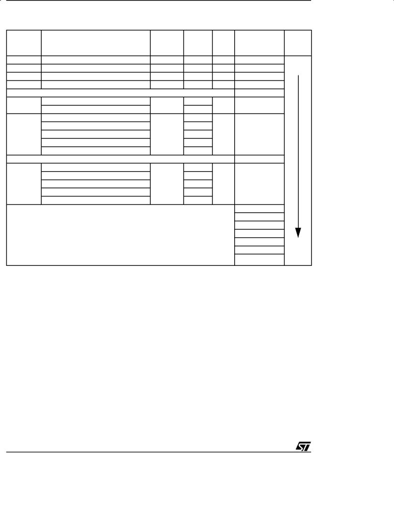
Table 5. Hardware Register Memory Map
Address |
Block |
Register |
Register name |
Reset Status |
Remarks |
|
Name |
Label |
|||||
|
|
|
|
|||
0000h |
|
PCDR |
Data Register |
00h |
R/W |
|
0001h |
Port C |
PCDDR |
Data Direction Register |
00h |
R/W |
|
0002h |
|
PCOR |
Option Register |
00h |
R/W |
|
0003h |
|
|
Reserved Area (1 Byte) |
|
|
|
0004h |
|
PBDR |
Data Register |
00h |
R/W |
|
0005h |
Port B |
PBDDR |
Data Direction Register |
00h |
R/W |
|
0006h |
|
PBOR |
Option Register |
00h |
R/W |
|
0007h |
|
|
Reserved Area (1 Byte) |
|
|
|
0008h |
|
PADR |
Data Register |
00h |
R/W |
|
0009h |
Port A |
PADDR |
Data Direction Register |
00h |
R/W |
|
000Ah |
|
PAOR |
Option Register |
00h |
R/W |
|
000Bh to |
|
|
Reserved Area (21 Bytes) |
|
|
|
001Fh |
|
|
|
|
||
|
|
|
|
|
||
0020h |
|
MISCR |
Miscellaneous Register |
00h |
R/W |
|
0021h |
|
SPIDR |
Data I/O Register |
xxh |
R/W |
|
0022h |
SPI |
SPICR |
Control Register |
0xh |
R/W |
|
0023h |
|
SPISR |
Status Register |
00h |
Read Only |
|
0024h |
WDG |
WDGCR |
Watchdog Control register |
7Fh |
R/W |
|
0025h to |
|
|
Reserved Area (12 Bytes) |
|
|
|
0030h |
|
|
|
|
||
|
|
|
|
|
||
0031h |
|
TACR2 |
Control Register2 |
00h |
R/W |
|
0032h |
|
TACR1 |
Control Register1 |
00h |
R/W |
|
0033h |
|
TASR |
Status Register |
00h |
Read Only |
|
0034h-0035h |
|
TAIC1HR |
Input Capture1 High Register |
xxh |
Read Only |
|
|
|
TAIC1LR |
Input Capture1 Low Register |
xxh |
Read Only |
|
0036h-0037h |
|
TAOC1HR |
Output Compare1 High Register |
80h |
R/W |
|
|
|
TAOC1LR |
Output Compare1 Low Register |
00h |
R/W |
|
0038h-0039h |
Timer A |
TACHR |
Counter High Register |
FFh |
Read Only |
|
|
|
TACLR |
Counter Low Register |
FCh |
Read Only |
|
003Ah-003Bh |
|
TAACHR |
Alternate Counter High Register |
FFh |
Read Only |
|
|
|
TAACLR |
Alternate Counter Low Register |
FCh |
Read Only |
|
003Ch-003Dh |
|
TAIC2HR |
Input Capture2 High Register |
xxh |
Read Only |
|
|
|
TAIC2LR |
Input Capture2 Low Register |
xxh |
Read Only |
|
003Eh-003Fh |
|
TAOC2HR |
Output Compare2 High Register |
80h |
R/W |
|
|
|
TAOC2LR |
Output Compare2 Low Register |
00h |
R/W |
|
0040h |
|
|
Reserved Area (1 Byte) |
|
|
11/84
ST72101/ST72212/ST72213
Block |
Register |
Register name |
Reset Status |
Remarks |
Address |
Label |
|||
Name |
|
|
|
|
0041h |
TBCR2 |
Control Register2 |
00h |
R/W |
0042h |
TBCR1 |
Control Register1 |
00h |
R/W |
0043h |
TBSR |
Status Register |
00h |
Read Only |
0044h-0045h |
TBIC1HR |
Input Capture1 High Register |
xxh |
Read Only |
|
TBIC1LR |
Input Capture1 Low Register |
xxh |
Read Only |
0046h-0047h |
TBOC1HR |
Output Compare1 High Register |
80h |
R/W |
0048h-0049h Timer B 1) |
TBOC1LR |
Output Compare1 Low Register |
00h |
R/W |
TBCHR |
Counter High Register |
FFh |
Read Only |
|
|
TBCLR |
Counter Low Register |
FCh |
Read Only |
004Ah-004Bh |
TBACHR |
Alternate Counter High Register |
FFh |
Read Only |
|
TBACLR |
Alternate Counter Low Register |
FCh |
Read Only |
004Ch-004Dh |
TBIC2HR |
Input Capture2 High Register |
xxh |
Read Only |
|
TBIC2LR |
Input Capture2 Low Register |
xxh |
Read Only |
004Eh-004Fh |
TBOC2HR |
Output Compare2 High Register |
80h |
R/W |
|
TBOC2LR |
Output Compare2 Low Register |
00h |
R/W |
0050h to |
|
Reserved Area (32 Bytes) |
|
|
006Fh |
|
|
|
|
|
|
|
|
|
0070h |
ADCDR |
Data Register |
00h |
Read Only |
ADC 2) |
ADCCSR |
Control/Status Register |
00h |
R/W |
0071h |
||||
0072h to |
|
|
|
|
007Fh
Reserved Area (14 Bytes)
Notes:
1.ST72212 only, reserved area for other devices.
2.ST72212 and ST72213 only, reserved otherwise.
12/84
ST72101/ST72212/ST72213
2 CENTRAL PROCESSING UNIT
2.1 INTRODUCTION
This CPU has a full 8-bit architecture and contains six internal registers allowing efficient 8-bit data manipulation.
2.2 MAIN FEATURES
■63 basic instructions
■Fast 8-bit by 8-bit multiply
■17 main addressing modes (with indirect addressing mode)
■Two 8-bit index registers
■16-bit stack pointer
■8 MHz CPU internal frequency
■Low power modes
■Maskable hardware interrupts
■Non-maskable software interrupt
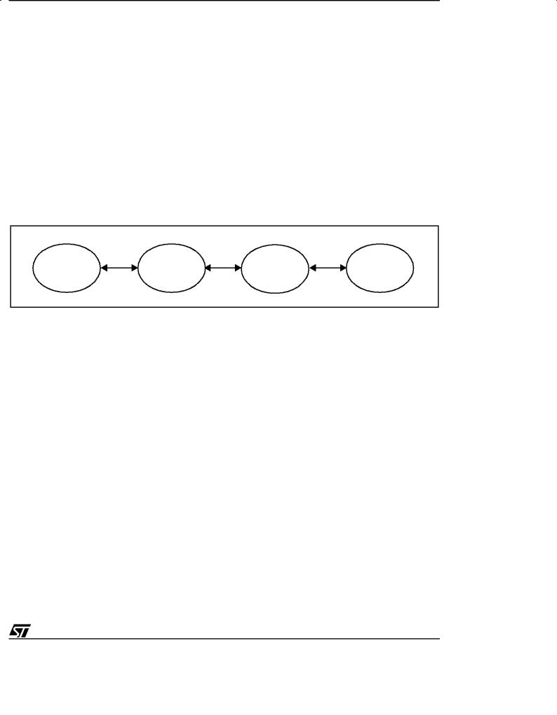
2.3 CPU REGISTERS
The 6 CPU registers shown in Figure 10 are not present in the memory mapping and are accessed by specific instructions.
Figure 10. CPU Registers
|
|
|
7 |
|
|
|
|
|
|
0 |
|
|
|
RESET VALUE = XXh |
|
||||||
|
|
|
7 |
|
|
|
|
|
|
0 |
|
|
|
RESET VALUE = XXh |
|
||||||
|
|
|
7 |
|
|
|
|
|
|
0 |
|
|
|
RESET VALUE = XXh |
|
||||||
15 |
PCH |
8 |
7 |
|
|
PCL |
|
|
0 |
|
RESET VALUE = RESET VECTOR @ FFFEh-FFFFh |
||||||||||
|
|
|
7 |
|
|
|
|
|
|
0 |
|
|
|
1 |
1 |
1 |
H |
I |
N |
Z |
C |
|
RESET VALUE = 1 |
1 |
1 |
X |
1 |
X |
X |
X |
||
15 |
|
8 |
7 |
|
|
|
|
|
|
0 |
RESET VALUE = STACK HIGHER ADDRESS
Accumulator (A)
The Accumulator is an 8-bit general purpose register used to hold operands and the results of the arithmetic and logic calculations and to manipulate data.
Index Registers (X and Y)
In indexed addressing modes, these 8-bit registers are used to create either effective addresses or temporary storage areas for data manipulation. (The Cross-Assembler generates a precede instruction (PRE) to indicate that the following instruction refers to the Y register.)
The Y register is not affected by the interrupt automatic procedures (not pushed to and popped from the stack).
Program Counter (PC)
The program counter is a 16-bit register containing the address of the next instruction to be executed by the CPU. It is made of two 8-bit registers PCL (Program Counter Low which is the LSB) and PCH (Program Counter High which is the MSB).
ACCUMULATOR
XINDEX REGISTER
YINDEX REGISTER
PROGRAM COUNTER
CONDITION CODE REGISTER
STACK POINTER
X = Undefined Value
13/84

ST72101/ST72212/ST72213
CENTRAL PROCESSING UNIT (Cont'd)
CONDITION CODE REGISTER (CC)
Read/Write
Reset Value: 111x1xxx
7 |
|
|
|
|
|
|
0 |
1 |
1 |
1 |
H |
I |
N |
Z |
C |
The 8-bit Condition Code register contains the interrupt mask and four flags representative of the result of the instruction just executed. This register can also be handled by the PUSH and POP instructions.
These bits can be individually tested and/or controlled by specific instructions.
Bit 4 = H Half carry.
This bit is set by hardware when a carry occurs between bits 3 and 4 of the ALU during an ADD or ADC instruction. It is reset by hardware during the same instructions.
0:No half carry has occurred.
1:A half carry has occurred.
This bit is tested using the JRH or JRNH instruction. The H bit is useful in BCD arithmetic subroutines.
Bit 3 = I Interrupt mask.
This bit is set by hardware when entering in interrupt or by software to disable all interrupts except the TRAP software interrupt. This bit is cleared by software.
0:Interrupts are enabled.
1:Interrupts are disabled.
This bit is controlled by the RIM, SIM and IRET instructions and is tested by the JRM and JRNM instructions.
Note: Interrupts requested while I is set are latched and can be processed when I is cleared. By default an interrupt routine is not interruptable because the I bit is set by hardware when you en-
ter it and reset by the IRET instruction at the end of the interrupt routine. If the I bit is cleared by software in the interrupt routine, pending interrupts are serviced regardless of the priority level of the current interrupt routine.
Bit 2 = N Negative.
This bit is set and cleared by hardware. It is representative of the result sign of the last arithmetic, logical or data manipulation. It is a copy of the 7th bit of the result.
0:The result of the last operation is positive or null.
1:The result of the last operation is negative
(i.e. the most significant bit is a logic 1).
This bit is accessed by the JRMI and JRPL instructions.
Bit 1 = Z Zero.
This bit is set and cleared by hardware. This bit indicates that the result of the last arithmetic, logical or data manipulation is zero.
0:The result of the last operation is different from zero.
1:The result of the last operation is zero.
This bit is accessed by the JREQ and JRNE test instructions.
Bit 0 = C Carry/borrow.
This bit is set and cleared by hardware and software. It indicates an overflow or an underflow has occurred during the last arithmetic operation.
0:No overflow or underflow has occurred.
1:An overflow or underflow has occurred.
This bit is driven by the SCF and RCF instructions and tested by the JRC and JRNC instructions. It is also affected by the ªbit test and branchº, shift and rotate instructions.
14/84
ST72101/ST72212/ST72213
CENTRAL PROCESSING UNIT (Cont'd)
Stack Pointer (SP)
Read/Write
Reset Value: 01 7Fh
15 |
|
|
|
|
|
|
8 |
0 |
0 |
0 |
0 |
0 |
0 |
0 |
1 |
7 |
|
|
|
|
|
|
0 |
0 |
1 |
SP5 |
SP4 |
SP3 |
SP2 |
SP1 |
SP0 |
The Stack Pointer is a 16-bit register which is always pointing to the next free location in the stack. It is then decremented after data has been pushed onto the stack and incremented before data is popped from the stack (see Figure 11).
Since the stack is 64 bytes deep, the 10 most significant bits are forced by hardware. Following an MCU Reset, or after a Reset Stack Pointer instruction (RSP), the Stack Pointer contains its reset value (the SP5 to SP0 bits are set) which is the stack higher address.
Figure 11. Stack Manipulation Example
CALL |
Interrupt |
PUSH Y |
Subroutine |
Event |
|
|
|
|
@ 0140h |
|
|
|
|
SP |
|
|
SP |
Y |
|
|
|
||
|
CC |
CC |
|
|
A |
A |
|
|
X |
X |
|
SP |
PCH |
PCH |
|
PCL |
PCL |
||
|
|||
PCH |
PCH |
PCH |
|
@ 017Fh PCL |
PCL |
PCL |
Stack Lower Address = 0140h
Stack Higher Address = 017Fh
The least significant byte of the Stack Pointer (called S) can be directly accessed by a LD instruction.
Note: When the lower limit is exceeded, the Stack Pointer wraps around to the stack upper limit, without indicating the stack overflow. The previously stored information is then overwritten and therefore lost. The stack also wraps in case of an underflow.
The stack is used to save the return address during a subroutine call and the CPU context during an interrupt. The user may also directly manipulate the stack by means of the PUSH and POP instructions. In the case of an interrupt, the PCL is stored at the first location pointed to by the SP. Then the other registers are stored in the next locations as shown in Figure 11.
±When an interrupt is received, the SP is decremented and the context is pushed on the stack.
±On return from interrupt, the SP is incremented and the context is popped from the stack.
A subroutine call occupies two locations and an interrupt five locations in the stack area.
POP Y |
IRET |
RET |
|
|
or RSP |
SP
CC |
|
|
A |
|
|
X |
|
|
PCH |
SP |
|
PCL |
||
|
||
PCH |
PCH |
|
PCL |
SP |
|
PCL |
15/84

ST72101/ST72212/ST72213
3 CLOCKS, RESET, INTERRUPTS & POWER SAVING MODES
3.1 CLOCK SYSTEM
3.1.1 General Description |
Figure 12. External Clock Source Connections |
The MCU accepts either a Crystal or Ceramic resonator, or an external clock signal to drive the internal oscillator. The internal clock (fCPU) is derived from the external oscillator frequency (fOSC).
The external Oscillator clock is first divided by 2, and division factor of 32 can be applied if Slow Mode is selected by setting the SMS bit in the Miscellaneous Register. This reduces the frequency of the fCPU; the clock signal is also routed to the on-chip peripherals.
The internal oscillator is designed to operate with an AT-cut parallel resonant quartz crystal resonator in the frequency range specified for fosc. The circuit shown in Figure 13 is recommended when using a crystal, and Table 6 lists the recommended capacitance and feedback resistance values. The crystal and associated components should be mounted as close as possible to the input pins in order to minimize output distortion and start-up stabilisation time.
Use of an external CMOS oscillator is recommended when crystals outside the specified frequency ranges are to be used.
Table 6. Recommended Values for 16 MHz Crystal Resonator (C0<7pF)
RSMAX |
40 Ω |
60 Ω |
150 Ω |
COSCIN |
56pF |
47pF |
22pF |
COSCOUT |
56pF |
47pF |
22pF |
C0: parasitic shunt capacitance of the quartz crystal.
RSMAX: equivalent serial resistor of the crystal (uper limit, see crystal specification).
COSCOUT, COSCIN: maximum total capacitance on OSCIN and OSCOUT, including the external ca-
pacitance plus the parasitic capacitance of the board and the device.
OSCIN OSCOUT
NC
EXTERNAL
CLOCK
Figure 13. Crystal/Ceramic Resonator
OSCIN OSCOUT
COSCIN |
COSCOUT |
Figure 14. Clock Prescaler Block Diagram
%2 |
% 16 |
|
|
fCPU |
|
OSCIN OSCOUT |
to CPU and |
|
Peripherals |
||
|
COSCIN |
C |
|
OSCOUT |
16/84
ST72101/ST72212/ST72213
3.2 RESET
3.2.1 Introduction
There are three sources of Reset:
±RESET pin (external source)
±Power-On Reset (Internal source)
±WATCHDOG (Internal Source)
The Reset Service Routine vector is located at address FFFEh-FFFFh.
3.2.2 External Reset
The RESET pin is both an input and an open-drain output with integrated pull-up resistor. When one of the internal Reset sources is active, the Reset
pin is driven low , for a duration of tRESET, to reset the whole application.
3.2.3 Reset Operation
The duration of the Reset state is a minimum of 4096 internal CPU Clock cycles. During the Reset state, all I/Os take their reset value.
A Reset signal originating from an external source
must have a duration of at least tPULSE in order to be recognised. This detection is asynchronous
and therefore the MCU can enter Reset state even in Halt mode.
At the end of the Reset cycle, the MCU may be held in the Reset state by an External Reset signal. The RESET pin may thus be used to ensure VDD has risen to a point where the MCU can operate correctly before the user program is run. Fol-
Figure 15. Reset Block Diagram
lowing a Reset event, or after exiting Halt mode, a 4096 CPU Clock cycle delay period is initiated in order to allow the oscillator to stabilise and to ensure that recovery has taken place from the Reset state.
In the high state, the RESET pin is connected internally to a pull-up resistor (RON). This resistor can be pulled low by external circuitry to reset the device.
The RESET pin is an asynchronous signal which plays a major role in EMS performance. In a noisy environment, it is recommended to use the external connections shown in Figure 8.
3.2.4 Power-on Reset
This circuit detects the ramping up of VDD, and generates a pulse that is used to reset the application (at approximately VDD= 2V).
Power-On Reset is designed exclusively to cope with power-up conditions, and should not be used in order to attempt to detect a drop in the power supply voltage.
Caution: to re-initialize the Power-On Reset, the power supply must fall below approximately 0.8V (Vtn), prior to rising above 2V. If this condition is not respected, on subsequent power-up the Reset pulse may not be generated. An external Reset pulse may be required to correctly reactivate the circuit.
OSCILLATOR
SIGNAL
TO ST7
RESET
RESET
VDD
RON
INTERNAL
RESET
COUNTER
POWER-ON RESET
WATCHDOG RESET
17/84

ST72101/ST72212/ST72213
3.3 INTERRUPTS
The ST7 core may be interrupted by one of two different methods: maskable hardware interrupts as listed in the Interrupt Mapping Table and a nonmaskable software interrupt (TRAP). The Interrupt processing flowchart is shown in Figure 16.
The maskable interrupts must be enabled clearing the I bit in order to be serviced. However, disabled interrupts may be latched and processed when they are enabled (see external interrupts subsection).
When an interrupt has to be serviced:
±Normal processing is suspended at the end of the current instruction execution.
±The PC, X, A and CC registers are saved onto the stack.
±The I bit of the CC register is set to prevent additional interrupts.
±The PC is then loaded with the interrupt vector of the interrupt to service and the first instruction of the interrupt service routine is fetched (refer to the Interrupt Mapping Table for vector addresses).
The interrupt service routine should finish with the IRET instruction which causes the contents of the saved registers to be recovered from the stack.
Note: As a consequence of the IRET instruction, the I bit will be cleared and the main program will resume.
Priority management
By default, a servicing interrupt can not be interrupted because the I bit is set by hardware entering in interrupt routine.
In the case several interrupts are simultaneously pending, an hardware priority defines which one will be serviced first (see the Interrupt Mapping Table).
Non Maskable Software Interrupts
This interrupt is entered when the TRAP instruction is executed regardless of the state of the I bit. It will be serviced according to the flowchart on Figure 16.
Interrupts and Low power mode
All interrupts allow the processor to leave the Wait low power mode. Only external and specific mentioned interrupts allow the processor to leave the
Halt low power mode (refer to the ªExit from HALTª column in the Interrupt Mapping Table).
External Interrupts
External interrupt vectors can be loaded in the PC register if the corresponding external interrupt occurred and if the I bit is cleared. These interrupts allow the processor to leave the Halt low power mode.
The external interrupt polarity is selected through the miscellaneous register or interrupt register (if available).
External interrupt triggered on edge will be latched and the interrupt request automatically cleared upon entering the interrupt service routine.
If several input pins, connected to the same interrupt vector, are configured as interrupts, their signals are logically ANDed before entering the edge/ level detection block.
Warning: The type of sensitivity defined in the Miscellaneous or Interrupt register (if available) applies to the EI source. In case of an ANDed source (as described on the I/O ports section), a low level on an I/O pin configured as input with interrupt, masks the interrupt request even in case of rising-edge sensitivity.
Peripheral Interrupts
Different peripheral interrupt flags in the status register are able to cause an interrupt when they are active if both:
±The I bit of the CC register is cleared.
±The corresponding enable bit is set in the control register.
If any of these two conditions is false, the interrupt is latched and thus remains pending.
Clearing an interrupt request is done by:
±writing ª0º to the corresponding bit in the status register or
±an access to the status register while the flag is set followed by a read or write of an associated register.
Note: the clearing sequence resets the internal latch. A pending interrupt (i.e. waiting for being enabled) will therefore be lost if the clear sequence is executed.
18/84

ST72101/ST72212/ST72213
INTERRUPTS (Cont'd)
Figure 16. Interrupt Processing Flowchart
FROM RESET
N |
|
BIT I SET |
|
Y |
N |
|
BIT I SET |
FETCH NEXT INSTR UCTION |
Y |
|
N
IRET
STACK PC, X, A, CC
Y SET I BIT
LOAD PC FROM INTERRUPT VECTOR
EXECUTE INSTRUCTION
RESTORE PC, X, A, CC FROM STACK
THIS CLEARS I BIT BY DEFAULT
19/84
ST72101/ST72212/ST72213
Table 7. Interrupt Mapping
Source |
|
Register |
|
Exit |
Vector |
|
Description |
Flag |
from |
||||
Block |
Label |
Address |
||||
|
|
HALT |
||||
|
|
|
|
|
||
RESET |
Reset |
N/A |
N/A |
yes |
FFFEh-FFF Fh |
|
TRAP |
Software |
N/A |
N/A |
no |
FFFCh-FFF Dh |
|
EI0 |
External Interrupt PA0:PA7 |
N/A |
N/A |
yes |
FFFAh-FFFBh |
|
EI1 |
External Interrupt PB0:PB7, PC0:PC5 |
N/A |
N/A |
yes |
FFF8h-FFF 9h |
|
|
Not Used |
|
|
|
FFF6h-FFF 7h |
|
SPI |
Transfer Complete |
SPISR |
SPIF |
no |
FFF4h-FFF 5h |
|
Mode Fault |
MODF |
|||||
|
|
|
|
|||
|
Input Capture 1 |
|
ICF1_A |
|
|
|
|
Output Compare 1 |
|
OCF1_A |
|
|
|
TIMER A |
Input Capture 2 |
TASR |
ICF2_A |
no |
FFF2h-FFF 3h |
|
|
Output Compare 2 |
|
OCF2_A |
|
|
|
|
Timer Overflow |
|
TOF_A |
|
|
|
|
Not Used |
|
|
|
FFF0h-FFF 1h |
|
|
Input Capture 1 |
|
ICF1_B |
|
|
|
|
Output Compare 1 |
|
OCF1_B |
|
|
|
TIMER B 1) |
Input Capture 2 |
TBSR |
ICF2_B |
no |
FFEEh-FFEFh |
|
|
Output Compare 2 |
|
OCF2_B |
|
|
|
|
Timer Overflow |
|
TOF_B |
|
|
|
|
|
|
|
|
FFECh-FFEDh |
|
|
|
|
|
|
FFEAh-FFEBh |
|
|
|
|
|
|
FFE8h-FFE9h |
|
|
Not Used |
|
|
|
FFE6h-FFE7h |
|
|
|
|
|
|
||
|
|
|
|
|
FFE4h-FFE5h |
|
|
|
|
|
|
FFE2h-FFE3h |
|
|
|
|
|
|
FFE0h-FFE1h |
Note 1: Timer B is available on ST72212 only.
Priority
Order
Highest
Priority
Lowest
Priority
20/84
3.4 POWER SAVING MODES
3.4.1 Introduction
There are three Power Saving modes. Slow Mode is selected by setting the relevant bits in the Miscellaneous register. Wait and Halt modes may be entered using the WFI and HALT instructions.
3.4.2 Slow Mode
In Slow mode, the oscillator frequency can be divided by a value defined in the Miscellaneous Register. The CPU and peripherals are clocked at this lower frequency. Slow mode is used to reduce power consumption, and enables the user to adapt clock frequency to available supply voltage.
3.4.3 Wait Mode
Wait mode places the MCU in a low power consumption mode by stopping the CPU. All peripherals remain active. During Wait mode, the I bit (CC Register) is cleared, so as to enable all interrupts. All other registers and memory remain unchanged. The MCU will remain in Wait mode until an Interrupt or Reset occurs, whereupon the Program Counter branches to the starting address of the Interrupt or Reset Service Routine.
The MCU will remain in Wait mode until a Reset or an Interrupt occurs, causing it to wake up.
Refer to Figure 17 below.
ST72101/ST72212/ST72213
Figure 17. WAIT Flow Chart
WFI INSTRUCTION
OSCILLATOR |
ON |
PERIPH. CLOCK |
ON |
CPU CLOCK |
OFF |
I-BIT |
CLEARED |
N
RESET
N
INTERRUPT |
Y |
|
|
|
|
||
Y |
OSCILLATOR |
ON |
|
PERIPH. CLOCK |
ON |
||
|
|||
|
CPU CLOCK |
ON |
|
|
I-BIT |
SET |
|
|
4096 CPU CLOCK |
||
|
CYCLES DELAY |
||
|
OSCILLATOR |
ON |
|
|
PERIPH. CLOCK |
ON |
|
|
CPU CLOCK |
ON |
|
|
I-BIT |
SET |
|
FETCH RESET VECTOR
OR SERVICE INTERRUPT
Note: Before servicing an interrupt, the CC register is pushed on the stack. The I-Bit is set during the interrupt routine and cleared when the CC register is popped.
21/84
ST72101/ST72212/ST72213
POWER SAVING MODES (Cont'd)
3.4.4 Halt Mode
The Halt mode is the MCU lowest power consumption mode. The Halt mode is entered by executing the HALT instruction. The internal oscillator is then turned off, causing all internal processing to be stopped, including the operation of the on-chip peripherals. The Halt mode cannot be used when the watchdog is enabled, if the HALT instruction is executed while the watchdog system is enabled, a watchdog reset is generated thus resetting the entire MCU.
When entering Halt mode, the I bit in the CC Register is cleared so as to enable External Interrupts. If an interrupt occurs, the CPU becomes active.
The MCU can exit the Halt mode upon reception of an interrupt or a reset. Refer to the Interrupt Mapping Table. The oscillator is then turned on and a stabilization time is provided before releasing CPU operation. The stabilization time is 4096 CPU clock cycles.
After the start up delay, the CPU continues operation by servicing the interrupt which wakes it up or by fetching the reset vector if a reset wakes it up.
Figure 18. HALT Flow Chart
|
|
HALT INSTRUCTION |
|
WATCHDOG |
Y |
WDG |
|
|
|
|
|
RESET |
|
ENABLED? |
|
|
|
|
|
|
|
N |
|
|
OSCILLATOR |
OFF |
|
|
PERIPH. CLOCK |
OFF |
|
|
CPU CLOCK |
OFF |
|
|
I-BIT |
CLEARED |
|
|
N |
|
|
|
|
RESET |
|
N |
|
|
|
EXTERNAL |
Y |
|
|
INTERRUPT1) |
|
||
Y |
|
OSCILLATOR |
ON |
|
|
||
|
|
PERIPH. CLOCK2) OFF |
|
|
|
CPU CLOCK |
ON |
|
|
I-BIT |
SET |
|
|
4096 CPU CLOCK |
|
|
|
CYCLES DELAY |
|
|
|
OSCILLATOR |
ON |
|
|
PERIPH. CLOCK |
ON |
|
|
CPU CLOCK |
ON |
|
|
I-BIT |
SET |
FETCH RESET VECTOR
OR SERVICE INTERRUPT
1)or some specific interrupts
2)if reset PERIPH. CLOCK = ON ; if interrupt PERIPH. CLOCK = OFF
Note: Before servicing an interrupt, the CC register is pushed on the stack. The I-Bit is set during the interrupt routine and cleared when the CC register is popped.
22/84
3.5 MISCELLANEOUS REGISTER
The Miscellaneous register allows to select the SLOW operating mode, the polarity of external interrupt requests and to output the internal clock.
Register Address: 0020h Ð Read/ Write
Reset Value: 0000 0000 (00h)
7 |
0 |
PEI3 PEI2 MCO PEI1 PEI0 - |
- SMS |
Bit 7:6 = PEI[3:2] External Interrupt EI1 Polarity
Option.
These bits are set and cleared by software. They determine which event on EI1 causes the external interrupt according to Table 8.
Table 8. EI1 External Interrupt Polarity Options
MODE |
PEI3 |
PEI2 |
|
Falling edge and low level |
0 |
0 |
|
(Reset state) |
|||
|
|
||
Falling edge only |
1 |
0 |
|
Rising edge only |
0 |
1 |
|
Rising and falling edge |
1 |
1 |
Note: Any modification of one of these two bits resets the interrupt request related to this interrupt vector.
Bit 5 = MCO Main Clock Out
This bit is set and cleared by software. When set, it enables the output of the Internal Clock on the PC2 I/O port.
0 - PC2 is a general purpose I/O port.
1 - MCO alternate function (fCPU is output on PC2 pin).
ST72101/ST72212/ST72213
Bit 4:3 = PEI[1:0] External Interrupt EI0 Polarity
Option.
These bits are set and cleared by software. They determine which event on EI0 causes the external interrupt according to Table 9.
Table 9. EI0 External Interrupt Polarity Options
MODE |
PEI1 |
PEI0 |
|
Falling edge and low level |
0 |
0 |
|
(Reset state) |
|||
|
|
||
Falling edge only |
1 |
0 |
|
Rising edge only |
0 |
1 |
|
Rising and falling edge |
1 |
1 |
Note: Any modification of one of these two bits resets the interrupt request related to this interrupt vector.
Bit 1:2 = Unused, always read at 0.
Warning: Software must write 1 to these bits for compatibility with future products.
Bit 0 = SMS Slow Mode Select
This bit is set and cleared by software.
0- Normal mode - fCPU = Oscillator frequency / 2 (Reset state)
1- Slow mode - fCPU = Oscillator frequency /32
23/84

ST72101/ST72212/ST72213
4 ON-CHIP PERIPHERALS
4.1 I/O PORTS
4.1.1 Introduction
The I/O ports offer different functional modes:
±transfer of data through digital inputs and outputs and for specific pins:
±analog signal input (ADC)
±alternate signal input/output for the on-chip peripherals.
±external interrupt generation
An I/O port is composed of up to 8 pins. Each pin can be programmed independently as digital input (with or without interrupt generation) or digital output.
4.1.2 Functional Description
Each port is associated to 2 main registers:
±Data Register (DR)
±Data Direction Register (DDR)
and some of them to an optional register:
± Option Register (OR)
Each I/O pin may be programmed using the corresponding register bits in DDR and OR registers: bit X corresponding to pin X of the port. The same correspondence is used for the DR register.
The following description takes into account the OR register, for specific ports which do not provide this register refer to the I/O Port Implementation Section 4.1.3. The generic I/O block diagram is shown on Figure 20.
4.1.2.1 Input Modes
The input configuration is selected by clearing the corresponding DDR register bit.
In this case, reading the DR register returns the digital value applied to the external I/O pin.
Different input modes can be selected by software through the OR register.
Notes:
1.All the inputs are triggered by a Schmitt trigger.
2.When switching from input mode to output mode, the DR register should be written first to output the correct value as soon as the port is con-
figured as an output.
Interrupt function
When an I/O is configured in Input with Interrupt, an event on this I/O can generate an external Interrupt request to the CPU. The interrupt polarity is given independently according to the description mentioned in the Miscellaneous register or in the interrupt register (where available).
Each pin can independently generate an Interrupt request.
Each external interrupt vector is linked to a dedicated group of I/O port pins (see Interrupts section). If several input pins are configured as inputs to the same interrupt vector, their signals are logically ANDed before entering the edge/level detection block. For this reason if one of the interrupt pins is tied low, it masks the other ones.
4.1.2.2 Output Mode
The pin is configured in output mode by setting the corresponding DDR register bit.
In this mode, writing ª0º or ª1º to the DR register applies this digital value to the I/O pin through the latch. Then reading the DR register returns the previously stored value.
Note: In this mode, the interrupt function is disabled.
4.1.2.3 Digital Alternate Function
When an on-chip peripheral is configured to use a pin, the alternate function is automatically selected. This alternate function takes priority over standard I/O programming. When the signal is coming from an on-chip peripheral, the I/O pin is automatically configured in output mode (push-pull or open drain according to the peripheral).
When the signal is going to an on-chip peripheral, the I/O pin has to be configured in input mode. In this case, the pin's state is also digitally readable by addressing the DR register.
Notes:
1.Input pull-up configuration can cause an unexpected value at the input of the alternate peripheral input.
2.When the on-chip peripheral uses a pin as input and output, this pin must be configured as an input (DDR = 0).
Warning: The alternate function must not be activated as long as the pin is configured as input with interrupt, in order to avoid generating spurious interrupts.
24/84
I/O PORTS (Cont'd)
4.1.2.4 Analog Alternate Function
When the pin is used as an ADC input the I/O must be configured as input, floating. The analog multiplexer (controlled by the ADC registers) switches the analog voltage present on the selected pin to the common analog rail which is connected to the ADC input.
It is recommended not to change the voltage level or loading on any port pin while conversion is in progress. Furthermore it is recommended not to have clocking pins located close to a selected analog pin.
Warning: The analog input voltage level must be within the limits stated in the Absolute Maximum Ratings.
ST72101/ST72212/ST72213
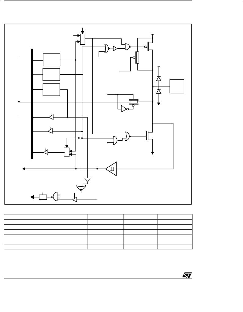
4.1.3 I/O Port Implementation
The hardware implementation on each I/O port depends on the settings in the DDR and OR registers and specific feature of the I/O port such as ADC Input (see Figure 20) or true open drain. Switching these I/O ports from one state to another should be done in a sequence that prevents unwanted side effects. Recommended safe transitions are illustrated in Figure 19. Other transitions are potentially risky and should be avoided, since they are likely to present unwanted side-effects such as spurious interrupt generation.
Figure 19. Recommended I/O State Transition Diagram |
|
|
|
INPUT |
INPUT |
OUTPUT |
OUTPUT |
with interrupt |
no interrupt |
open-drain |
push-pull |
|
|
||
25/84
ST72101/ST72212/ST72213
I/O PORTS (Cont'd)
Figure 20. I/O Block Diagram
ALTERNATE ENABLE
ANALOG RAIL |
DATA BUS |
COMMON |
|
ALTERNATE 1 |
M |
|
VDD |
OUTPUT |
|
|
|
U |
|
|
|
|
|
|
|
0 |
X |
|
P-BUFFER |
|
|
||
|
|
|
(SEE TABLE BELOW) |
DR |
|
ALTERNATE |
PULL-UP |
LATCH |
|
ENABLE |
|
|
|
|
PULL-UP |
VDD |
|
DDR |
DIODE |
||
CONDITION |
|||
(SEE TABLE BELOW) |
|||
LATCH |
|||
|
|||
|
|
||
OR |
|
PAD |
|
ANALOG ENABLE |
|
||
LATCH |
|
||
|
|
||
(SEE TABLE BELOW) |
(ADC) |
|
|
|
|
||
|
ANALOG |
GND |
|
OR SEL |
|
||
SWITCH |
|
||
|
|
||
|
(SEE NOTE BELOW) |
|
|
DDR SEL |
|
|
|
|
|
N-BUFFER |
|
|
ALTERNATE |
|
|
|
DR SEL |
1 |
ENABLE |
|
|
|
|
|
M |
|
|
|
|
|
|
U |
|
|
|
|
|
|
X |
|
GND |
|
|
|
|
0 |
|
|
|
|
ALTERNATE INPUT |
|
|
|
|
|
|
|
|
|
CMOS |
|
|
|
|
POLARITY |
FROM |
SCHMITT TRIGGER |
|
|
EXTERNAL |
SEL |
|
|
|
||
OTHER |
|
|
|
|||
|
|
|
|
|||
INTERRUPT |
|
BITS |
|
|
|
|
SOURCE (EIx) |
|
|
|
|
|
|
Table 10. Port Mode Configuration |
|
|
|
|||
|
Configu ration Mode |
Pull-up |
P-buffer |
VDD Diode |
||
Floating |
|
|
0 |
0 |
1 |
|
Pull-up |
|
|
1 |
0 |
1 |
|
Push-pull |
|
|
0 |
1 |
1 |
|
True Open Drain |
|
|
not present |
not present |
not present in OTP |
|
|
|
and EPROM devices |
||||
|
|
|
|
|
|
|
Open Drain (logic level) |
|
0 |
0 |
1 |
||
Legend: |
|
|
Notes: |
|
|
|
0 - |
present, not activated |
|
± No OR Register on some ports (see register map). |
|||
1 - |
present and activated |
|
± ADC Switch on ports with analog alternate functions. |
|||
26/84
 Loading...