


M29F002BT70P1
SGS Thomson Microelectronics M29F002BT70P1, M29F002BT70N1, M29F002BT70K6, M29F002BT70K1T, M29F002BT70K1 Datasheet
...
1/22
PRELIMINARY DATA
October 1999
This is preliminary information on a new product now in development or undergoing evaluation. Details are subject to change without notice.
M29F002BT
M29F002BB, M29F002BNT
2 Mbit (256Kb x8, Boot Block) Single Supply Flash Memory
■ SINGLE 5V ± 10% SUPPLY VOLTAGE for
PROGRAM, ERASE and READ OPERATIONS
■ ACCESS TIME: 45ns
■ PROGRAMMING TIME
–8µs by Byte typical
■ 7 MEMORY BLOCKS
– 1 Boot Block (Top or Bottom Location)
– 2 Parameter and 4 Main Blocks
■ PROGRAM/ERASE CONTROLLER
– Embedded Byte Program algorithm
– Embedded Multi-Block/Chip Erase algorithm
– Status Register Polling and Toggle Bits
■ ERASE SUSPEND and RESUME MODES
– Read and Program another Block during
Erase Suspend
■ UNLOCK BYPASS PROGRAM COMMAND
– Faster Production/Batch Programming
■ TEMPORARY BLOCK UNPROTECTION
MODE
■ LOW POWER CONSUMPTION
– Standby and Automatic Standby
■ 100,000 PROGRAM/ERASE CYCLES per
BLOCK
■ 20 YEARS DATA RETENTION
– Defectivity below 1 ppm/year
■ ELECTRONIC SIGNATURE
– Manufacturer Code: 20h
– M29F002BT Device Code: B0h
– M29F002BNT Device Code: B0h
– M29F002BB Device Code: 34h
32
1
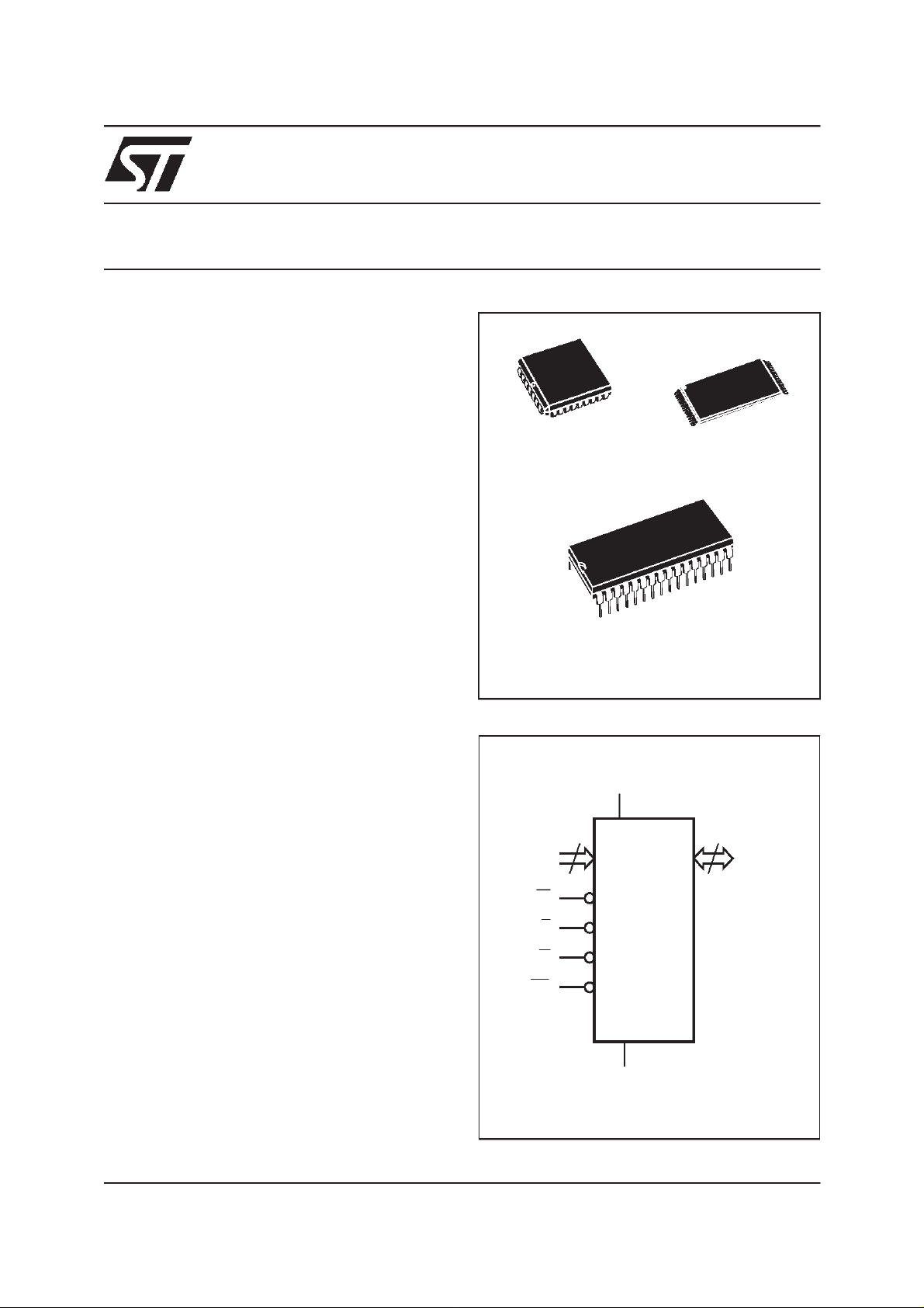
TSOP32 (N)
8 x 20mm
PLCC32 (K)
PDIP32 (P)
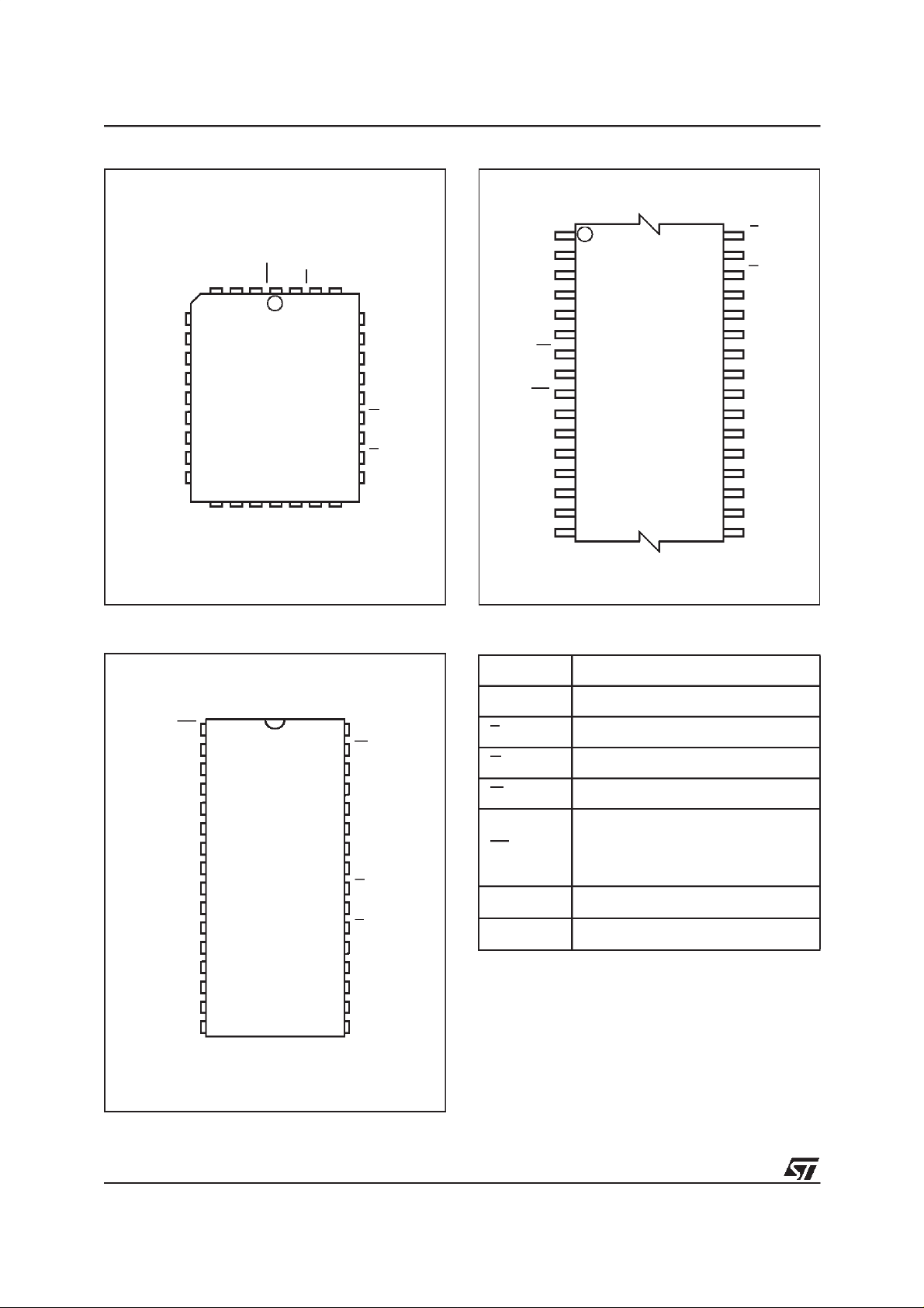
Figure 1. Logic Diagram
AI02957
18
A0-A17
W
DQ0-DQ7
V
CC
M29F002BT
M29F002BB
M29F002BNT
E
V
SS
8
G
RP
M29F002BT, M29F002BB, M29F002BNT
2/22
Figure 2A. PLCC Connections
AI02959
A17
A13
A10
DQ5
17
A1
A0
DQ0
DQ1
DQ2
DQ3
DQ4
A7
A4
A3
A2
A6
A5
9
W
A8
1
A16
A9
DQ7
A12
A14
32
RP
V
CC
M29F002BT
M29F002BB
A15
A11
DQ6
G
E
25
V
SS
Table 1. Signal Names
A0-A17 Address Inputs
DQ0-DQ7 Data Inputs/Outputs
E Chip Enable
G Output Enable
W Write Enable
RP
M29F002BB, M29F002BT:
Reset/Block Temporary Unprotect
M29F002NBT:
Not Connected Internally
V
CC
Supply Voltage
V
SS
Ground
SUMMARY DESCRIPTION
The M29F002B is a 2Mbit (256Kb x8) non-volatile
memory that can be read, erased and repro-
grammed. Theseoperations can be performedus-
ing a single 5V supply. On power-up the memory
defaults to its Read mode where it can be read in
the same way as a ROM or EPROM. The
M29F002B is fully backward compatible with the
M29F002.
Figure 2B. TSOP Connections
A1
A0
DQ0
A7
A4 A3
A2
A6
A5
A13
A10
A8
A9
DQ7
A14
A11 G
E
DQ5
DQ1
DQ2
DQ3
DQ4
DQ6
A17
W
A16
A12
RP
V
CC
A15
AI02958
M29F002BT
M29F002BB
8
1
9
16 17
24
25
32
V
SS
Figure 2C. PDIP Connections
A1
A0
DQ0
A7
A4
A3
A2
A6
A5
A13
A10
A8
A9
DQ7
A14
A11
G
E
DQ5DQ1
DQ2
DQ3V
SS
DQ4
DQ6
A17
WA16
A12
RP V
CC
A15
AI02960
M29F002BT
M29F002BB
M29F002BNT
8
1
2
3
4
5
6
7
9
10
11
12
13
14
15
16
32
31
30
29
28
27
26
25
24
23
22
21
20
19
18
17
3/22
M29F002BT, M29F002BB, M29F002BNT
The memory is divided into blocks that can be
erased independently so it is possible to preserve
valid data while old data is erased. Eachblock can
be protected independently to prevent accidental
Program or Erase commands from modifying the
memory. Program and Erase commands are writ-
ten to the Command Interface of the memory. An
on-chip Program/Erase Controller simplifies the
process ofprogramming orerasing thememory by
taking care of all of the special operations that are
required to update the memory contents. The end
of a program or erase operation can be detected
and any error conditions identified. The command
set required to control the memory is consistent
with JEDEC standards.
The blocks in the memory are asymmetrically ar-
ranged, see Tables 3A and 3B, Block Addresses.
The first or last 64 Kbytes have been divided into
four additional blocks. The 16 Kbyte Boot Block
can beused forsmall initialization codeto startthe
microprocessor, the two 8 Kbyte Parameter
Blocks can be used for parameter storage and the
remaining 32K is a small MainBlock wherethe ap-
plication may be stored.
Chip Enable, OutputEnable andWrite Enable sig-
nals control the bus operation of the memory.
They allow simple connection to most micropro-
cessors, often without additional logic.
The memory is offered in TSOP32 (8 x 20mm),
PLCC32 and PDIP packages. Access times of
45ns, 55ns, 70ns, 90ns and 120ns are available.
The memory is supplied with all the bits erased
(set to ’1’).
SIGNAL DESCRIPTIONS
See Figure 1, Logic Diagram, and Table 1, Signal
Names, for abrief overview of thesignals connect-
ed to this device.
Address Inputs (A0-A17). The Address Inputs
select the cells in the memory array toaccess dur-
ing BusRead operations. During BusWrite opera-
tions they control the commands sent to the
Command Interface of the internal state machine.
Data Inputs/Outputs (DQ0-DQ7). The Data In-
puts/Outputs output thedata stored at theselected
address during a Bus Read operation. During Bus
Write operations they represent the commands
sentto theCommand Interface ofthe internal state
machine.
Chip Enable (E). The Chip Enable, E, activates
the memory, allowing BusRead and Bus Write op-
erations to be performed. When Chip Enable is
High, V
IH
, all other pins are ignored.
Output Enable (G). The Output Enable, G, con-
trols the Bus Read operation of the memory.
Write Enable (W). The Write Enable, W, controls
the Bus Write operation of the memory’s Com-
mand Interface.
Reset/Block Temporary Unprotect(RP). The Re-
set/Block TemporaryUnprotect pin can be usedto
apply a Hardware Reset to the memory or to tem-
porarily unprotect all blocks that have been pro-
tected. On the M29F002BNT the pin is not
connected internally and this feature is not avail-
able.
Table 2. Absolute Maximum Ratings
(1)
Note: 1. Except for the rating ”Operating Temperature Range”, stresses above those listed in the Table ”Absolute Maximum Ratings” may
cause permanent damage to the device. These are stress ratings only and operation of the device atthese or any other conditions
above those indicated in the Operating sections of this specification is not implied. Exposure to Absolute Maximum Rating condi-
tions forextended periods may affect device reliability. Refer also tothe STMicroelectronics SURE Program and other relevantqual-
ity documents.
2. Minimum Voltage may undershoot to –2V during transition and for less than 20ns during transitions.
Symbol Parameter Value Unit
T
A
Ambient Operating Temperature (Temperature Range Option 1) 0 to 70 °C
Ambient Operating Temperature (Temperature Range Option 6) –40 to 85 °C
Ambient Operating Temperature (Temperature Range Option 3) –40 to 125 °C
T
BIAS
Temperature Under Bias –50 to 125 °C
T
STG
Storage Temperature –65 to 150 °C
V
IO
(2)
Input or Output Voltage –0.6 to 6 V
V
CC
Supply Voltage –0.6 to 6 V
V
ID
Identification Voltage –0.6 to 13.5 V

M29F002BT, M29F002BB, M29F002BNT
4/22
Table 3A. M29F002BT, M29F002BNT Block
Addresses
Size (Kbytes) Address Range
16 3C000h-3FFFFh
8 3A000h-3BFFFh
8 38000h-39FFFh
32 30000h-37FFFh
64 20000h-2FFFFh
64 10000h-1FFFFh
64 00000h-0FFFFh
A Hardware Reset is achieved by holding Reset/
Block Temporary Unprotect Low, V
IL
, for at least
t
PLPX
. After Reset/Block Temporary Unprotect
goes High, V
IH
, the memory will be ready for Bus
Read and Bus Write operations after t
PHEL
or t
PLYH
, whichever occurs last. See Table 14 and
Figure 10, Reset/Temporary Unprotect AC Char-
acteristics for more details.
Holding RP at V
ID
will temporarily unprotect the
protected blocks in the memory. Program and
Erase operations on all blocks will be possible.
The transition from V
IH
toV
ID
must be slower than
t
PHPHH
.
Reset/Block Temporary Unprotect can be left un-
connected. A weak internal pull-up resistor en-
sures that the memory always operates correctly.
V
CC
Supply Voltage. The V
CC
Supply Voltage
supplies the power for all operations (Read, Pro-
gram, Erase etc.).
The Command Interface is disabled whenthe V
CC
Supply Voltage is less than the Lockout Voltage,
V
LKO
. Thisprevents BusWrite operationsfrom ac-
cidentally damaging the data during power up,
power down and power surges. If the Program/
Erase Controller is programming or erasingduring
this time then the operation aborts and the memo-
ry contents being altered will be invalid.
A 0.1µF capacitor should be connected between
the V
CC
Supply Voltage pin and the V
SS
Ground
pin to decouple the current surges from the power
supply. The PCB trackwidths must be sufficient to
carry the currents required during program and
erase operations, I
CC4
.
V
SS
Ground. TheV
SS
Groundis the reference for
all voltage measurements.
BUS OPERATIONS
There are five standard bus operations thatcontrol
the device. These are Bus Read, Bus Write, Out-
put Disable,Standby and Automatic Standby. See
Table 4, BusOperations, for asummary. Typically
glitches of less than 5ns on Chip Enable or Write
Enable are ignored by the memory and do not af-
fect bus operations.
Bus Read. Bus Read operations read from the
memory cells, or specific registers in the Com-
mand Interface. A valid Bus Read operation in-
volves settingthe desired address on the Address
Inputs, applying a Low signal, V
IL
, to Chip Enable
and Output Enable and keeping Write Enable
High, V
IH
. The Data Inputs/Outputs will output the
value, see Figure 7, Read Mode AC Waveforms,
and Table11, Read ACCharacteristics, for details
of when the output becomes valid.
Bus Write. Bus Write operations write to the
Command Interface. A valid Bus Write operation
begins by setting the desired address on the Ad-
dress Inputs. The Address Inputs are latched by
the Command Interface onthe falling edgeof Chip
Enable or Write Enable, whichever occurs last.
The Data Inputs/Outputs are latched by the Com-
mand Interface on the rising edge of Chip Enable
or Write Enable,whichever occursfirst.OutputEn-
able must remain High, V
IH
, during the whole Bus
Write operation. See Figures 8 and 9, Write AC
Waveforms, and Tables 12 and 13, Write AC
Characteristics, for details of the timing require-
ments.
Output Disable. The Data Inputs/Outputs are in
the high impedance state when Output Enable is
High, V
IH
.
Table 3B. M29F002BB Block Addresses
Size (Kbytes) Address Range
64 30000h-3FFFFh
64 20000h-2FFFFh
64 10000h-1FFFFh
32 08000h-0FFFFh
8 06000h-07FFFh
8 04000h-05FFFh
16 00000h-03FFFh
5/22
M29F002BT, M29F002BB, M29F002BNT
Table 4. Bus Operations
Note: X = V
IL
or V
IH
.
Operation E G W Address Inputs
Data
Inputs/Outp uts
Bus Read
V
IL
V
IL
V
IH
Cell Address Data Output
Bus Write
V
IL
V
IH
V
IL
Command Address Data Input
Output Disable X
V
IH
V
IH
X Hi-Z
Standby
V
IH
X X X Hi-Z
Read Manufacturer
Code
V
IL
V
IL
V
IH
A0 = V
IL
,A1=V
IL
,A9=V
ID
,
Others V
IL
or V
IH
20h
Read Device Code V
IL
V
IL
V
IH
A0 = V
IH
,A1=V
IL
,A9=V
ID
,
Others V
IL
or V
IH
B0h (M29F002BT)
B0h (M29F002BNT)
34h (M29F002BB)
Standby. When Chip Enable is High, V
IH
, the
Data Inputs/Outputs pins are placed in the high-
impedance state and the Supply Current is re-
duced to the Standby level.
When Chip Enable is at V
IH
the Supply Current is
reduced to the TTL Standby Supply Current, I
CC2
.
To furtherreduce the SupplyCurrent tothe CMOS
Standby Supply Current, I
CC3
, ChipEnable should
be held within V
CC
± 0.2V. For Standby current
levels see Table 10, DC Characteristics.
During program or erase operations the memory
will continue to use the Program/Erase Supply
Current, I
CC4
, forProgram or Eraseoperations un-
til the operation completes.
AutomaticStandby. If CMOSlevels (V
CC
± 0.2V)
are usedto drive thebus and the busis inactivefor
150ns or more the memory enters Automatic
Standby where the internal Supply Current is re-
duced tothe CMOS Standby Supply Current,I
CC3
.
The Data Inputs/Outputs will still output data if a
Bus Read operation is in progress.
Special Bus Operations
Additional bus operations can be performed to
read the Electronic Signature and also to apply
and remove Block Protection. These bus opera-
tions are intended for use by programming equip-
ment and are not usually used in applications.
They require V
ID
to be applied to some pins.
Electronic Signature. The memory has two
codes, the manufacturer code and the device
code, that can be read to identify the memory.
These codes can be read by applying the signals
listed in Table 4, Bus Operations.
Block Protection and Blocks Unprotection. Each
block can be separately protected against acci-
dental Program or Erase. Protected blocks can be
unprotected to allow data to be changed.
There are two methods available for protecting
and unprotecting the blocks, one for use on pro-
gramming equipment and the other for in-system
use. For further information refer to Application
Note AN1122, Applying Protection and Unprotec-
tion to M29 Series Flash.

M29F002BT, M29F002BB, M29F002BNT
6/22
COMMAND INTERFACE
All Bus Write operations to the memory are inter-
preted by the Command Interface. Commands
consist of one or more sequential Bus Write oper-
ations. Failure to observe a valid sequence of Bus
Write operations will result in the memory return-
ing to Read mode. The long command sequences
are imposed to maximize data security.
The commands are summarized in Table 5, Com-
mands. Refer to Table 5 in conjunction with the
text descriptions below.
Read/Reset Command. The Read/Reset com-
mand returns the memory toits Read modewhere
it behaves like a ROM or EPROM. It also resets
the errors in the Status Register. Either one or
three Bus Write operations can be used to issue
the Read/Reset command.
If the Read/Reset command is issued during a
Block Eraseoperation or followinga Programming
or Erase error then the memory will takeupto 10µs
to abort. During the abort period no valid data can
be read from the memory. Issuing a Read/Reset
command during a Block Erase operation will
leave invalid data in the memory.
Auto Select Command. The Auto Select com-
mand is used to read the Manufacturer Code, the
Device Code and the Block Protection Status.
Three consecutive Bus Write operations are re-
quired to issue the Auto Select command. Once
the Auto Select command is issued the memory
remains in Auto Select mode until another com-
mand is issued.
From the Auto Select mode the Manufacturer
Code can be read using a Bus Read operation
with A0 = V
IL
and A1 = V
IL
. The otheraddress bits
may be set to either V
IL
or V
IH
. The Manufacturer
Code for STMicroelectronics is 20h.
The Device Code can be read using a Bus Read
operation with A0 = V
IH
and A1 = V
IL
. The other
address bits may be set to either V
IL
or V
IH
.The
Device Code for the M29F002BT is B0h, the
M29F002BNT is B0h and the M29F002BB is 34h.
The Block Protection Status of each block can be
read using a Bus Read operation with A0 = V
IL
,
A1 = V
IH
, and A13-A17 specifying the address of
the block. The otheraddress bits may be set toei-
ther V
IL
or V
IH
. If the addressed block is protected
then 01his output on the Data Inputs/Outputs,oth-
erwise 00h is output.
Program Command. The Program command
can be used to program a value to one address in
the memory array at a time. The command re-
quires fourBus Write operations, the final writeop-
eration latchesthe address and data inthe internal
state machine and starts the Program/Erase Con-
troller.
If the address falls in a protected block then the
Program command is ignored, the data remains
unchanged. The Status Registeris never read and
no error condition is given.
During the program operation the memory will ig-
nore all commands. It is not possible to issue any
command to abort or pause the operation. Typical
program timesare given in Table 6. Bus Read op-
erations during the program operation will output
the Status Register on the Data Inputs/Outputs.
See the section on the Status Register for more
details.
After the program operation has completed the
memory will return to the Read mode, unless an
error has occurred. When an error occurs the
memory will continue to output the Status Regis-
ter. A Read/Reset command must beissued to re-
set the error condition and return to Read mode.
Note thatthe Program command cannotchange a
bit set at ’0’ backto ’1’ and attempting to do so will
cause anerror. One of the Erase Commands must
be used to set all thebits in a blockor in the whole
memory from ’0’ to ’1’.
Unlock Bypass Command. The Unlock Bypass
command is used in conjunction with the Unlock
Bypass Programcommand to program the memo-
ry. When the access time to the device is long (as
with some EPROM programmers) considerable
time saving can be made by using these com-
mands. Three Bus Write operations are required
to issue the Unlock Bypass command.
Once the Unlock Bypass command has been is-
sued the memory will only accept the Unlock By-
pass Program command and the Unlock Bypass
Reset command. The memory can be read asif in
Read mode.
Unlock Bypass Program Command. The Un-
lock Bypass Program command can be used to
program one address in memory at a time. The
command requires two Bus Write operations, the
final write operation latches the address and data
in the internal state machine and starts the Pro-
gram/Erase Controller.
The Program operation using the Unlock Bypass
Program command behaves identically tothe Pro-
gram operation using the Program command. A
protected block cannot be programmed; the oper-
ation cannotbe aborted and theStatus Register is
read. Errors must be reset using the Read/Reset
command, which leaves the device in Unlock By-
pass Mode. See the Program command for details
on the behavior.
7/22
M29F002BT, M29F002BB, M29F002BNT
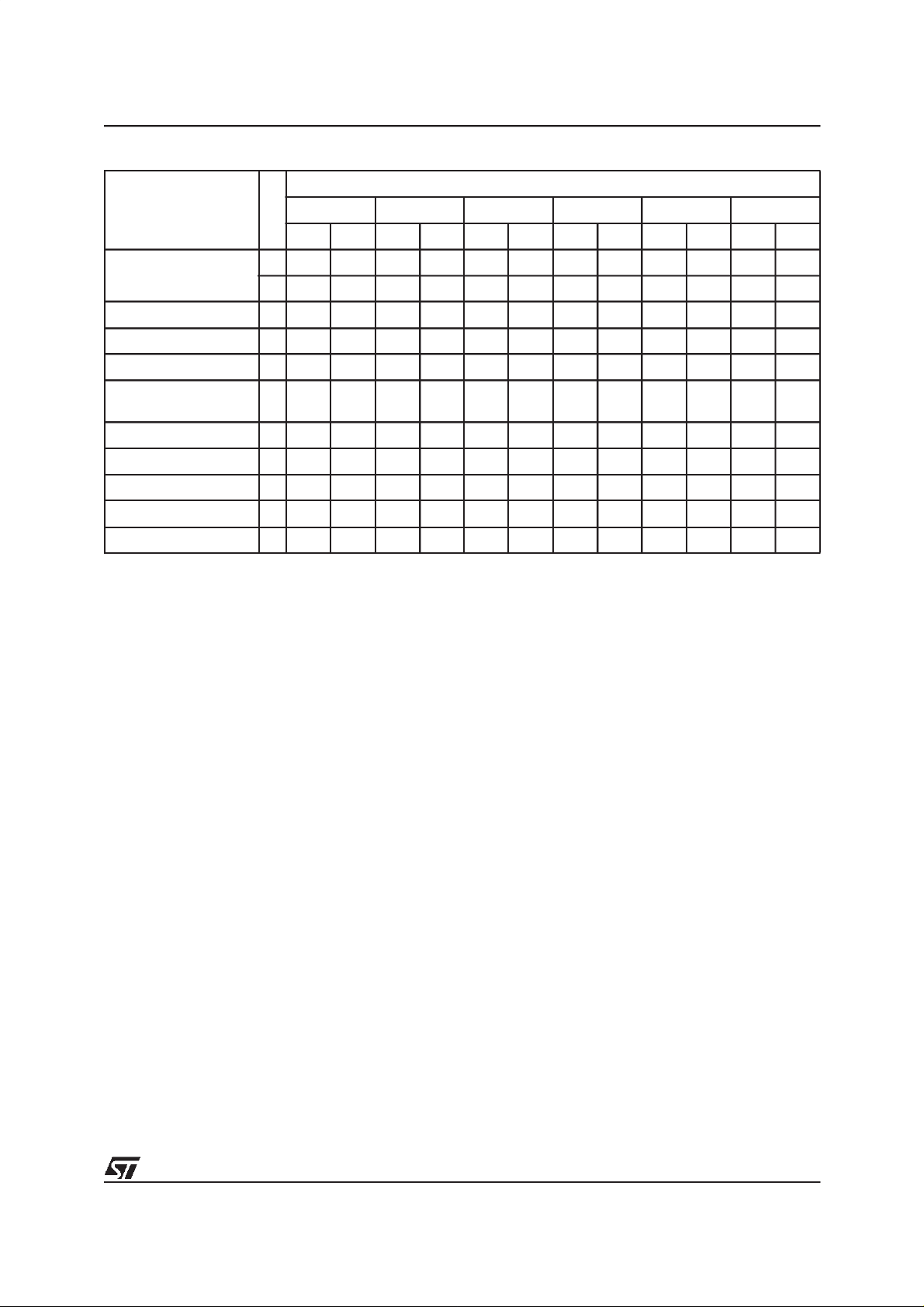
Table 5. Commands
Note: X Don’t Care, PA Program Address, PD Program Data, BA Any address in the Block.
All values in the table are in hexadecimal.
The Command Interface only uses address bits A0-A10 to verify the commands, the upper address bits are Don’t Care.
Read/Reset. After a Read/Reset command, read the memory as normal until another command is issued.
Auto Select. After an Auto Select command, readManufacturer ID, Device ID or Block Protection Status.
Program, Unlock Bypass Program, Chip Erase, BlockErase. After these commands read the Status Register until the Program/Erase
Controller completes and the memory returns to Read Mode. Add additional Blocks during Block Erase Command with additional Bus Write
Operations until the Timeout Bit is set.
Unlock Bypass. After the Unlock Bypass command issue Unlock Bypass Program or Unlock Bypass Reset commands.
Unlock Bypass Reset. After the Unlock Bypass Reset command read the memory asnormal until another command is issued.
Erase Suspend. After the EraseSuspend command readnon-erasing memory blocks as normal, issue Auto Select and Program commands
on non-erasing blocks as normal.
Erase Resume. After the Erase Resume command the suspended Erase operation resumes, read the Status Register until the Program/
Erase Controller completes and the memory returns to Read Mode.
Command
Length
Bus Write Operations
1st 2nd 3rd 4th 5th 6th
Addr Data Addr Data Addr Data Addr Data Addr Data Addr Data
Read/Reset
1X F0
3 555 AA 2AA 55 X F0
Auto Select 3 555 AA 2AA 55 555 90
Program 4 555 AA 2AA 55 555 A0 PA PD
Unlock Bypass 3 555 AA 2AA 55 555 20
Unlock Bypass
Program
2X A0PAPD
Unlock Bypass Reset 2 X 90 X 00
Chip Erase 6 555 AA 2AA 55 555 80 555 AA 2AA 55 555 10
Block Erase 6+ 555 AA 2AA 55 555 80 555 AA 2AA 55 BA 30
Erase Suspend 1 X B0
Erase Resume 1 X 30
Unlock Bypass Reset Command. The Unlock
Bypass Reset command can be used to return to
Read/Reset mode from Unlock Bypass Mode.
Two BusWrite operations are required to issuethe
Unlock Bypass Reset command.
Chip Erase Command. The Chip Erase com-
mand canbeused to erase the entire chip. SixBus
Write operations are required to issue the Chip
Erase Command and start the Program/Erase
Controller.
If any blocks are protected then these are ignored
and all the other blocks are erased. If all of the
blocks are protected the ChipErase operation ap-
pears tostart but will terminate within about100µs,
leaving the data unchanged. No error condition is
given when protected blocks are ignored.
During the erase operation the memory will ignore
all commands. It is not possible to issueany com-
mand to abort the operation. Typical chip erase
times are given in Table 6. All Bus Read opera-
tions during the Chip Erase operation will output
the Status Register on the Data Inputs/Outputs.
See the section on the Status Register for more
details.
After the Chip Erase operation has completed the
memory will return to the Read Mode, unless an
error has occurred. When an error occurs the
memory will continue to output the Status Regis-
ter. A Read/Reset command must beissued to re-
set the error condition and return to Read Mode.
TheChip Erase Command setsall of the bits in un-
protected blocks of the memory to ’1’. All previous
data is lost.
 Loading...