


ST62T10CM6
SGS Thomson Microelectronics ST62T10CM6, ST62T20CM6, ST62T20CM3, ST62T20CB6, ST62T20CB3 Datasheet
...
September 1998 1/70
Rev. 2.6
ST62T08C/T0 9C
ST62T10C/T20C/E20C
8-BIT OTP/EPROM MCUs WITH A/D CONVERTER,
OSCILLATOR SAFEGUARD, SAFE RESET AND 20 PINS
■
3.0 to 6.0V Supply Operating Range
■
8 MHz Maximum Clock Frequency
■
-40 to +125°C Operating Temperature Range
■
Run, Wait and Stop Modes
■
5 Interrupt Vectors
■
Look-up Table capability in Program Memory
■
Data Storage in Program Memory:
User selectable size
■
Data RAM: 64bytes
■
User Programmable Options
■
12 I/O pins, fully programmable as:
– Input with pull-up resistor
– Input without pull-up resistor
– Input with interrupt generation
– Open-drain or push-pull output
– Analog Input (except ST62T08C)
■
4 I/O lines can sink up to 20mA to drive LEDs or
TRIACs directly
■
8-bit Timer/Counter with 7-bit programmable
prescaler
■
Digital Watchdog
■
Oscillator Safe Guard
■
Low Voltage Detector for Safe Reset
■
8-bit A/D Converter with up to 8 analog inputs
■
On-chip Clock oscillator can be driven by Quartz
Crystal Ceramic resonator or RC network
■
Power-on Reset
■
One external Non-Maskable Interrupt
■
ST626x-EMU2 Emulation and Development
System (connects to an MS-DOS PC via a
parallel port)
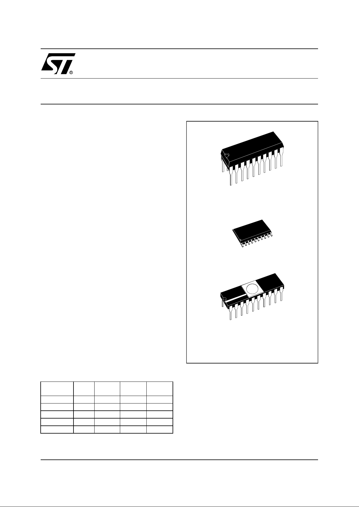
DEVICE SUMMARY
PDIP20
PSO20
CDIP20W
(See end of Datasheet for Ordering Information)
DEVICE
OTP
(Bytes)
EPROM
(Bytes)
I/O Pins
Analog
inputs
ST62T08C 1036 - 12 ST62T09C 1036 - 12 4
ST62T10C 1836 - 12 8
ST62T20C 3884 - 12 8
ST62E20C - 3884 12 8
89

2/70
Table of Contents
70
Document
Page
90
ST62T08C/T09C/ST62T10C/T20C/E20C . . . . . . . . . . . . . . . . . . 1
1 GENERAL DESCRIPTION . . . . . . . . . . . . . . . . . . . . . . . . . . . . . . . . . . . . . . . . . . . . . . . . . . . . . . 4
1.1 INTRODUCTION . . . . . . . . . . . . . . . . . . . . . . . . . . . . . . . . . . . . . . . . . . . . . . . . . . . . . . . . . 4
1.2 PIN DESCRIPTIONS . . . . . . . . . . . . . . . . . . . . . . . . . . . . . . . . . . . . . . . . . . . . . . . . . . . . . . 5
1.3 MEMORY MAP . . . . . . . . . . . . . . . . . . . . . . . . . . . . . . . . . . . . . . . . . . . . . . . . . . . . . . . . . . 6
1.3.1 Introduction . . . . . . . . . . . . . . . . . . . . . . . . . . . . . . . . . . . . . . . . . . . . . . . . . . . . . . . . 6
1.3.2 Program Space . . . . . . . . . . . . . . . . . . . . . . . . . . . . . . . . . . . . . . . . . . . . . . . . . . . . . 7
1.3.3 Data Space . . . . . . . . . . . . . . . . . . . . . . . . . . . . . . . . . . . . . . . . . . . . . . . . . . . . . . . . 8
1.3.4 Stack Space . . . . . . . . . . . . . . . . . . . . . . . . . . . . . . . . . . . . . . . . . . . . . . . . . . . . . . . . 8
1.3.5 Data Window Register (DWR) . . . . . . . . . . . . . . . . . . . . . . . . . . . . . . . . . . . . . . . . . . 9
1.4 PROGRAMMING MODES . . . . . . . . . . . . . . . . . . . . . . . . . . . . . . . . . . . . . . . . . . . . . . . . . 10
1.4.1 Option Bytes . . . . . . . . . . . . . . . . . . . . . . . . . . . . . . . . . . . . . . . . . . . . . . . . . . . . . . 10
1.4.2 Program Memory . . . . . . . . . . . . . . . . . . . . . . . . . . . . . . . . . . . . . . . . . . . . . . . . . . . 11
1.4.3 EPROM Erasing . . . . . . . . . . . . . . . . . . . . . . . . . . . . . . . . . . . . . . . . . . . . . . . . . . . . 11
2 CENTRAL PROCESSING UNIT . . . . . . . . . . . . . . . . . . . . . . . . . . . . . . . . . . . . . . . . . . . . . . . . . 12
2.1 INTRODUCTION . . . . . . . . . . . . . . . . . . . . . . . . . . . . . . . . . . . . . . . . . . . . . . . . . . . . . . . . 12
2.2 CPU REGISTERS . . . . . . . . . . . . . . . . . . . . . . . . . . . . . . . . . . . . . . . . . . . . . . . . . . . . . . . 12
3 CLOCKS, RESET, INTERRUPTS AND POWER SAVING MODES . . . . . . . . . . . . . . . . . . . . . 14
3.1 CLOCK SYSTEM . . . . . . . . . . . . . . . . . . . . . . . . . . . . . . . . . . . . . . . . . . . . . . . . . . . . . . . . 14
3.1.1 Main Oscillator . . . . . . . . . . . . . . . . . . . . . . . . . . . . . . . . . . . . . . . . . . . . . . . . . . . . . 14
3.1.2 Low Frequency Au xiliar y Os cillat or (LFA O) . . . . . . . . . . . . . . . . . . . . . . . . . . . . . . . 15
3.1.3 Oscillator Safe Guard . . . . . . . . . . . . . . . . . . . . . . . . . . . . . . . . . . . . . . . . . . . . . . . . 15
3.2 RESETS . . . . . . . . . . . . . . . . . . . . . . . . . . . . . . . . . . . . . . . . . . . . . . . . . . . . . . . . . . . . . . . 18
3.2.1 RESET Input . . . . . . . . . . . . . . . . . . . . . . . . . . . . . . . . . . . . . . . . . . . . . . . . . . . . . . 18
3.2.2 Power-on Reset . . . . . . . . . . . . . . . . . . . . . . . . . . . . . . . . . . . . . . . . . . . . . . . . . . . . 18
3.2.3 Watchdog Reset . . . . . . . . . . . . . . . . . . . . . . . . . . . . . . . . . . . . . . . . . . . . . . . . . . . 19
3.2.4 LVD Reset . . . . . . . . . . . . . . . . . . . . . . . . . . . . . . . . . . . . . . . . . . . . . . . . . . . . . . . . 19
3.2.5 Application Notes . . . . . . . . . . . . . . . . . . . . . . . . . . . . . . . . . . . . . . . . . . . . . . . . . . . 19
3.2.6 MCU Initialization Sequence . . . . . . . . . . . . . . . . . . . . . . . . . . . . . . . . . . . . . . . . . . 20
3.3 DIGITAL WATCHDOG . . . . . . . . . . . . . . . . . . . . . . . . . . . . . . . . . . . . . . . . . . . . . . . . . . . . 22
3.3.1 Digital Watchdog Register (DWDR) . . . . . . . . . . . . . . . . . . . . . . . . . . . . . . . . . . . . . 24
3.3.2 Application Notes . . . . . . . . . . . . . . . . . . . . . . . . . . . . . . . . . . . . . . . . . . . . . . . . . . . 24
3.4 INTERRUPTS . . . . . . . . . . . . . . . . . . . . . . . . . . . . . . . . . . . . . . . . . . . . . . . . . . . . . . . . . . 26
3.4.1 Interrupt request . . . . . . . . . . . . . . . . . . . . . . . . . . . . . . . . . . . . . . . . . . . . . . . . . . . . 26
3.4.2 Interrupt Procedure . . . . . . . . . . . . . . . . . . . . . . . . . . . . . . . . . . . . . . . . . . . . . . . . . 27
3.4.3 Interrupt Option Register (IOR) . . . . . . . . . . . . . . . . . . . . . . . . . . . . . . . . . . . . . . . . 28
3.4.4 Interrupt Sources . . . . . . . . . . . . . . . . . . . . . . . . . . . . . . . . . . . . . . . . . . . . . . . . . . . 28
3.5 POWER SAVING MODES . . . . . . . . . . . . . . . . . . . . . . . . . . . . . . . . . . . . . . . . . . . . . . . . . 30
3.5.1 WAIT Mode . . . . . . . . . . . . . . . . . . . . . . . . . . . . . . . . . . . . . . . . . . . . . . . . . . . . . . . 30
3.5.2 STOP Mode . . . . . . . . . . . . . . . . . . . . . . . . . . . . . . . . . . . . . . . . . . . . . . . . . . . . . . . 30
3.5.3 Exit from WAIT and STOP Modes . . . . . . . . . . . . . . . . . . . . . . . . . . . . . . . . . . . . . . 31
4 ON-CHIP PERIPHERALS . . . . . . . . . . . . . . . . . . . . . . . . . . . . . . . . . . . . . . . . . . . . . . . . . . . . . . 32
4.1 I/O PORTS . . . . . . . . . . . . . . . . . . . . . . . . . . . . . . . . . . . . . . . . . . . . . . . . . . . . . . . . . . . . . 32
4.1.1 Operating Modes . . . . . . . . . . . . . . . . . . . . . . . . . . . . . . . . . . . . . . . . . . . . . . . . . . . 33
4.1.2 Safe I/O State Switching Sequence . . . . . . . . . . . . . . . . . . . . . . . . . . . . . . . . . . . . . 34
4.1.3 I/O Port Option Registers . . . . . . . . . . . . . . . . . . . . . . . . . . . . . . . . . . . . . . . . . . . . . 35

3/70
Table of Contents
Document
Page
91
4.1.4 I/O Port Data Direction Registers . . . . . . . . . . . . . . . . . . . . . . . . . . . . . . . . . . . . . . . 35
4.1.5 I/O Port Data Registers . . . . . . . . . . . . . . . . . . . . . . . . . . . . . . . . . . . . . . . . . . . . . . 35
4.2 TIMER . . . . . . . . . . . . . . . . . . . . . . . . . . . . . . . . . . . . . . . . . . . . . . . . . . . . . . . . . . . . . . . . 37
4.2.1 Timer Operating Modes . . . . . . . . . . . . . . . . . . . . . . . . . . . . . . . . . . . . . . . . . . . . . . 38
4.2.2 Timer Interrupt . . . . . . . . . . . . . . . . . . . . . . . . . . . . . . . . . . . . . . . . . . . . . . . . . . . . . 38
4.2.3 Application Notes . . . . . . . . . . . . . . . . . . . . . . . . . . . . . . . . . . . . . . . . . . . . . . . . . . . 39
4.2.4 Timer Registers . . . . . . . . . . . . . . . . . . . . . . . . . . . . . . . . . . . . . . . . . . . . . . . . . . . . 39
4.3 A/D CONVERTER (ADC) . . . . . . . . . . . . . . . . . . . . . . . . . . . . . . . . . . . . . . . . . . . . . . . . . 40
4.3.1 Application Notes . . . . . . . . . . . . . . . . . . . . . . . . . . . . . . . . . . . . . . . . . . . . . . . . . . . 40
5 SOFTWARE . . . . . . . . . . . . . . . . . . . . . . . . . . . . . . . . . . . . . . . . . . . . . . . . . . . . . . . . . . . . . . . . 42
5.1 ST6 ARCHITECTURE . . . . . . . . . . . . . . . . . . . . . . . . . . . . . . . . . . . . . . . . . . . . . . . . . . . . 42
5.2 ADDRESSING MODES . . . . . . . . . . . . . . . . . . . . . . . . . . . . . . . . . . . . . . . . . . . . . . . . . . . 42
5.3 INSTRUCTION SET . . . . . . . . . . . . . . . . . . . . . . . . . . . . . . . . . . . . . . . . . . . . . . . . . . . . . . 43
6 ELECTRICAL CHARACTERISTICS . . . . . . . . . . . . . . . . . . . . . . . . . . . . . . . . . . . . . . . . . . . . . . 48
6.1 ABSOLUTE MAXIMUM RATINGS . . . . . . . . . . . . . . . . . . . . . . . . . . . . . . . . . . . . . . . . . . . 48
6.2 RECOMMENDED OPERATING CONDITIONS . . . . . . . . . . . . . . . . . . . . . . . . . . . . . . . . . 49
6.3 DC ELECTRICAL CHARACTERISTICS . . . . . . . . . . . . . . . . . . . . . . . . . . . . . . . . . . . . . . 50
6.4 AC ELECTRICAL CHARACTERISTICS . . . . . . . . . . . . . . . . . . . . . . . . . . . . . . . . . . . . . . 51
6.5 A/D CONVERTER CHARACTERISTICS . . . . . . . . . . . . . . . . . . . . . . . . . . . . . . . . . . . . . . 52
6.6 TIMER CHARACTERISTICS . . . . . . . . . . . . . . . . . . . . . . . . . . . . . . . . . . . . . . . . . . . . . . . 52
7 GENERAL INFORMATION . . . . . . . . . . . . . . . . . . . . . . . . . . . . . . . . . . . . . . . . . . . . . . . . . . . . . 58
7.1 PACKAGE MECHANICAL DATA . . . . . . . . . . . . . . . . . . . . . . . . . . . . . . . . . . . . . . . . . . . . 58
7.2 .ORDERING INFORMATION . . . . . . . . . . . . . . . . . . . . . . . . . . . . . . . . . . . . . . . . . . . . . . . 59
ST62P08C/P09C/ST62P10C/P20C . . . . . . . . . . . . . . . . . . . . . . 61
1 GENERAL DESCRIPTION . . . . . . . . . . . . . . . . . . . . . . . . . . . . . . . . . . . . . . . . . . . . . . . . . . . . . 62
1.1 INTRODUCTION . . . . . . . . . . . . . . . . . . . . . . . . . . . . . . . . . . . . . . . . . . . . . . . . . . . . . . . . 62
1.2 ORDERING INFORMATION . . . . . . . . . . . . . . . . . . . . . . . . . . . . . . . . . . . . . . . . . . . . . . . 62
1.2.1 Transfer of Customer Code . . . . . . . . . . . . . . . . . . . . . . . . . . . . . . . . . . . . . . . . . . . 62
1.2.2 Listing Generation and Verification . . . . . . . . . . . . . . . . . . . . . . . . . . . . . . . . . . . . . 62
ST6208C/09C/ST6210C/20C . . . . . . . . . . . . . . . . . . . . . . . . . . . 65
1 GENERAL DESCRIPTION . . . . . . . . . . . . . . . . . . . . . . . . . . . . . . . . . . . . . . . . . . . . . . . . . . . . . 66
1.1 INTRODUCTION . . . . . . . . . . . . . . . . . . . . . . . . . . . . . . . . . . . . . . . . . . . . . . . . . . . . . . . . 66
1.2 ROM READOUT PROTECTION . . . . . . . . . . . . . . . . . . . . . . . . . . . . . . . . . . . . . . . . . . . . 66
1.3 ORDERING INFORMATION . . . . . . . . . . . . . . . . . . . . . . . . . . . . . . . . . . . . . . . . . . . . . . . 68
1.3.1 Transfer of Customer Code . . . . . . . . . . . . . . . . . . . . . . . . . . . . . . . . . . . . . . . . . . . 68
1.3.2 Listing Generation and Verification . . . . . . . . . . . . . . . . . . . . . . . . . . . . . . . . . . . . . 68
4/70
ST62T08C/T09C ST62T10C/T20C/E20 C
1 GENERAL DESCRIPTIO N
1.1 INTRODUCTION
The ST62T08C,T09C,T10C,T20C and ST62E20C
devices are low cost members of the ST62xx 8-bit
HCMOS family of microcontrollers, which is targeted at low to medium complexity applications. All
ST62xx devices are based on a building block approach: a common core is surrounded by a
number of on-chip peripherals.
The ST62E20C is the erasable EPROM version of
the ST62T08C,T09C,T10C and T20C device,
which may be used to emulate the
ST62T08C,T09C,T10C and T20C device, as well
as the respective ST6208C,09C,10C,20C ROM
devices.
OTP and E PROM dev ices are func tionally identical. The ROM based versions offer the same func-
tionality selecting as ROM opt ions t he op tio ns defined in the programmable option bytes of the
OTP/EPROM versions.
OTP devices offer all the advant ages of user programmability at low cost, which make them the
ideal choice in a wide range of applications where
frequent code chang es, mul tiple code vers ions or
last minute programmability are required.
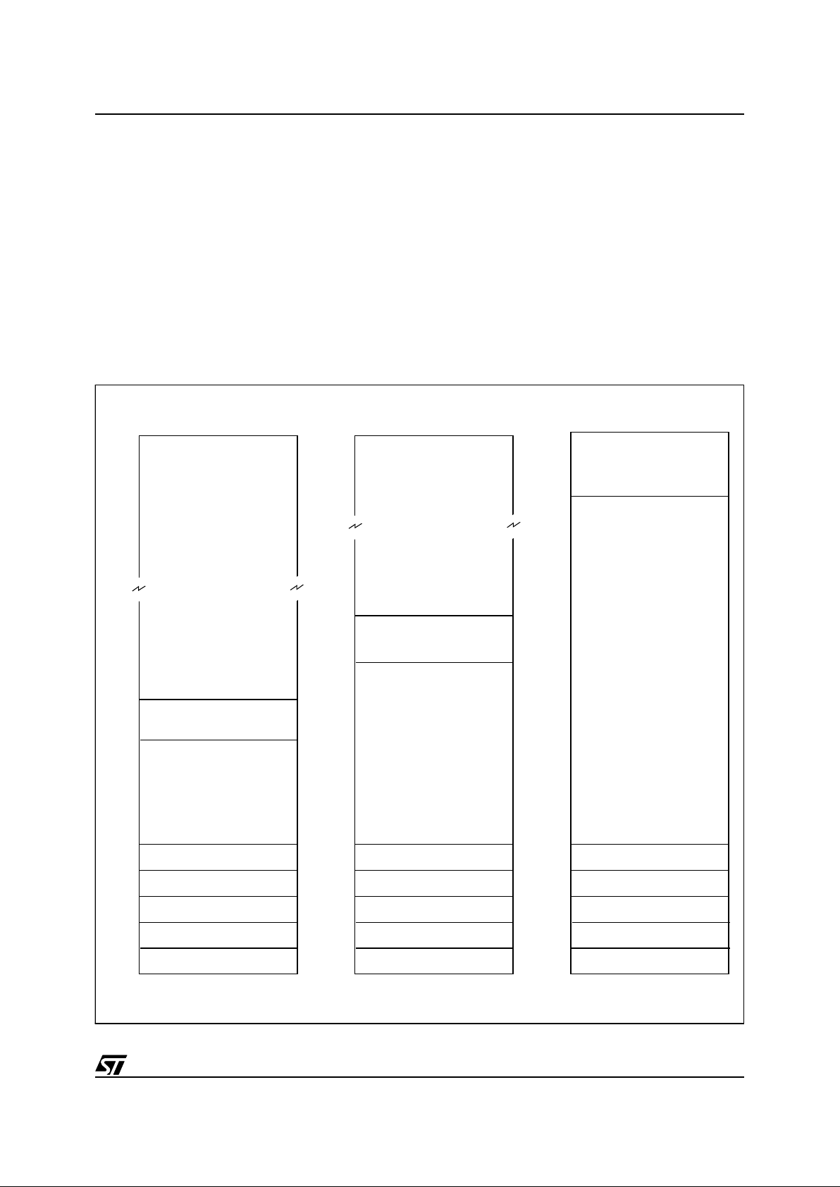
These compact low-cost devices feature a Timer
comprising an 8-bit counter and a 7-bit programmable prescaler,an 8-bit A/ D Co nve rter with u p t o
8 analog inputs and a Digital Watchdog timer,
making them well suited for a wide range of automotive, appliance and industrial applications.
Figure 1. Bloc k D ia gram
TEST
NMI
INTERRUPT
PROGRAM
1836 Bytes
PC
STACK LEVEL 1
STACK LEVEL 2
STACK LEVEL 3
STACK LEVEL 4
STACK LEVEL 5
STACK LEVEL 6
POWER
SUPPLY
OSCILLATOR
RESET
DATA ROM
USER
SELECTABLE
DATA RAM
64 Bytes
PORT A
PORT B
TIMER
DIGITAL
8 BIT CORE
TEST/V
PP
3884 Bytes
(ST62T10C)
(ST62T20C, E20C)
8-BIT
A/D CONVERTER
PA0..PA3 (20mA Sink)
TIMER
V
DDVSS
OSCin O SCou t RESET
WATCHDOG
:
MEMORY
PB0..PB7 / Ain (*)
1036 Byt es
(ST62T08C,T09C)
(*) Analog input availability depend on versions
92
5/70
ST62T08C/T09C ST62T10C/T20C /E20C
1.2 PIN DESCRIPTIONS
V
DD
and V
SS
. Power is supplied to the MCU via
these two pins. V
DD
is the power conn ection and
V
SS
is the ground connection.
OSCin and OSCout.
These pins are internally
connected to the on-chip oscillator circuit. A quartz
crystal, a ceramic resonator or an external clock
signal can be connected between these two pins.
The OSCin pin is the input pin, the O SCout pin is
the output pin.
RESET
. The active-low RESET pin is used to restart the microcontroller. Internal pull-up is p rovided at this pin.
TEST/V
PP
.
The TEST must be held a t V
SS
for normal operation. If TEST pin is connected to a
+12.5V level during the reset phase, the EPROM
programming Mode is entered.
NMI.
The NMI pin provides the capability for asynchronous interruption, by applying an external non
maskable interrupt to the MCU. The NM I input is
falling edge sensitive. The user can select as option the availability of an on-chip pull-up at this pin.
TIMER.
This is the timer I/O pin. In input mode it is
connected to the prescaler and acts as external
timer clock input or as control gate input for the internal timer clock. In output mode the timer pin outputs the data bit when a time-out occurs. The user
can selec t as option the availability of an on-chip
pull-up at this pin.
PA0-PA3.
These 4 lines are organized as one I/O
port (A). Each line may be configu red under software control as inputs with or without internal pullup resistors, interrupt generating inputs with pull-
up resistors, open-drain or push-pull outputs. PA0PA3 can also sink 20mA for direct LED driving.
PB0-PB7.
These 8 lines are organized as one I/O
port (B). Each line may be configured under software control as inputs with or without internal pullup resistors, interrupt generating inputs with pullup resistors, open-drain or push-pull outputs. PB0PB3 can be u sed as analog inp ut to the A /D converter on the ST62T10C , T20C and E20C, while
PB4-PB7 can be used as analog inputs for the A/D
converter on the ST62T09C, T10C, T20C and
E20C.
Figure 2. ST62T08C,T09C, T10C, T20C and
E20C Pin Configurat io n
1
2
3
4
5
6
7
8
9
10
11
12
13
14
15
16
17
18
19
20
V
DD
TIMER
OSCin
OSCout
NMI
V
PP
/TEST
RESET
Ain*/PB7
Ain*/PB6
Ain*/PB5
V
SS
PA0/20 mA Sink
PA1/20 mA Sink
PA2/20 mA Sink
PA3/20 mA Sink
PB0/Ain*
PB1/Ain*
PB2/Ain*
PB3/Ain*
PB4/Ain*
*Analog input availability depend on device
93
6/70
ST62T08C/T09C ST62T10C/T20C/E20 C
1.3 MEMORY MAP
1.3.1 Introduction
The MCU operates in three separate memory
spaces: Program space, Data space, and Stack
space. Operation in these three memory spaces is
described in the following paragraphs.
Briefly, Program space contains user program
code in OTP and user vectors; Data space contains user data in RAM and in OTP, and Stack
space accommodat es six levels of stack for subroutine and interrupt service routine nesting.
Figure 3. Me m ory A ddressing D iagram
PROGRAM SPAC E
PROGRAM
INTERRUPT &
RESET VECTORS
ACCUMULATOR
DATA RAM
BANK SELECT
WINDOW SELECT
RAM
X REGISTER
Y REGISTER
V REGISTER
W REGISTER
DATA READ-ONLY
WINDOW
RAM / EEPROM
BANKING AREA
000h
03Fh
040h
07Fh
080h
081h
082h
083h
084h
0C0h
0FFh
0-63
DATA SPACE
0000h
0FF0h
0FFFh
MEMORY
MEMORY
DATA READ-ONLY
MEMORY
94
7/70
ST62T08C/T09C ST62T10C/T20C /E20C
MEMORY MAP
(Cont’d)
1.3.2 Program Space
Program Space comprises the instructions to be
executed, the data required for immediate addressing mode instructions, the reserved factory
test area and the user v ectors. Program Space is
addressed via the 12-bit Program Counter register
(PC register)Program Memory Protection.
The Program Mem ory in O TP o r EP ROM devices
can be protected against external readout of memory by selecting the READOUT PROTECTION option in the option byte.
In the EPROM parts, READOUT PROTECTION
option can be disactivated only by U.V. erasure
that also results into the whole EPROM context
erasure.
Note:
Once the Readout Protection is activated, it
is no longer possible, even for STMicroelectronics,
to gain access to the OTP contents. Returned
parts with a protection set can therefore not be accepted.
Figure 4. Program Memo ry Map
(*) Reserved areas should be filled with 0FFh
0000h
0AFFh
0B00h
0B9Fh
NOT IMPLEMENTED
RESERVED
*
USER
PROGRAM MEMORY
(OTP)
1024 BYTES
0BA0h
0F9Fh
0FA0h
0FEFh
0FF0h
0FF7h
0FF8h
0FFBh
0FFCh
0FFDh
0FFEh
0FFFh
RESERVED
*
RESERVED
INTERRUPT VECTORS
NMI VECTOR
USER RESET VECTOR
0000h
07Fh
USER
PROGRAM MEMORY
(OTP/EPROM)
3872 BYTES
080h
0F9Fh
0FA0h
0FEFh
0FF0h
0FF7h
0FF8h
0FFBh
0FFCh
0FFDh
0FFEh
0FFFh
RESERVED
*
RESERVED
*
INTERRUPT VECTORS
NMI VECTOR
USER RESET VECTOR
RESERVED
*
0000h
07FFh
0800h
087Fh
NOT IMPLEMENTED
RESERVED
*
USER
PROGRAM MEMORY
(OTP)
1824 BYTES
0880h
0F9Fh
0FA0h
0FEFh
0FF0h
0FF7h
0FF8h
0FFBh
0FFCh
0FFDh
0FFEh
0FFFh
RESERVED
*
RESERVED
INTERRUPT VECTORS
NMI VECTOR
USER RESET VECTOR
ST62T08C,T 09C ST62T10C ST62T20C,E20C
95

8/70
ST62T08C/T09C ST62T10C/T20C/E20 C
MEMORY MAP
(Cont’d)
1.3.3 Data Space
Data Space accommodates all the data necessary
for processing the user program. This space comprises the RAM resource, the proces sor core and
peripheral registers, as well as read-only data
such as constants and look-up tables in OTP/
EPROM.
1.3.3.1 Data ROM
All read-only data is physically stored in program
memory, which also accommodates the Program
Space. The program memory cons equently contains the program code to be executed, as well as
the constants and look-up tables required by the
application.
The Data Space locations in which the different
constants and look-up tables are addressed by the
processor core may be thought of as a 64-byte
window through which it is possible to access the
read-only data stored in OTP/EPROM.
1.3.3.2 Data RAM
In ST6208C/09C/10C/20C devices, the data
space includes 60 bytes of RAM , the ac cumu lator
(A), the indirect registers (X), (Y), the short direct
registers (V), (W), the I/O port registers, the peripheral data and control registers, the interrupt
option register and the Data ROM Window register
(DRW register).
1.3.4 Stack Space
Stack space consists of six 12-bit registers which
are used to stack subroutine and interrupt return
addresses, as well as the current program counter
contents.
Table 1. ST6208C/09C/10C/20C Data Memory
Space
RESERVED
000h
03Fh
DATA RO M WINDOW A REA
64 BYTES
040h
07Fh
X REGISTER 080h
Y REGISTER 081h
V REGISTER 082h
W REGISTER 083h
DATA RAM 60 BYTES
084h
0BFh
PORT A DATA REGISTER 0C0h
PORT B DATA REGISTER 0C1h
RESERVED 0C2h
RESERVED 0C3h
PORT A DIRECTION REGISTER 0C4h
PORT B DIRECTION REGISTER 0C5h
RESERVED 0C6h
RESERVED 0C7h
INTERRUP T OP T ION REGISTER 0C8h*
DATA ROM WINDOW REGISTER 0C9h*
RESERVED
0CAh
0CBh
PORT A OPTION REGISTER 0CCh
PORT B OPTION REGISTER 0CDh
RESERVED 0CEh
RESERVED 0CFh
A/D DATA REG I ST ER(ex ce pt ST62T08C) 0D0h
A/D CONTROL REGISTER (except ST62T08C) 0D1h
TIMER PRESCALER REGISTER 0D2h
TIMER COUNTER REGISTER 0D3h
TIMER S TA T US CO NT ROL REGIST E R 0D4h
RESERVED
0D5h
0D6h
0D7h
WATCHD O G REG I ST ER 0D8h
RESERVED
0D9h
0FEh
ACCUMULATOR 0FFh
* WRITE ONLY REGISTE R
96
9/70
ST62T08C/T09C ST62T10C/T20C /E20C
MEMORY MAP
(Cont’d)
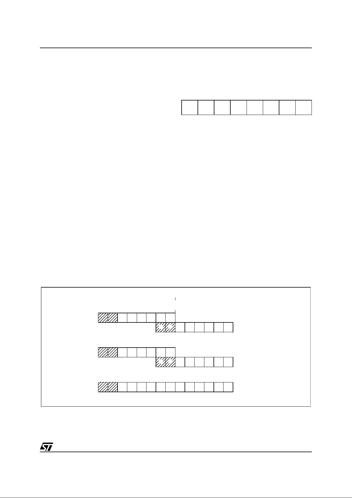
1.3.5 Data Window Register (DWR)
The Data read-only memory window is located from
address 0040h to address 007Fh in Data space. It
allows direct reading of 64 consecutive bytes located anywhere in program memory, between address 0000h and 0FFFh (top memory address depends on the specific device). All the program
memory can therefore be used to store ei ther instructions or read-only data. Indeed, the window
can be moved i n steps of 64 byt es along the program memory by writing the appropriate code in the
Data Window Register (DWR).
The DWR can be addressed like any RAM location
in the Data Space, it is however a write-only register and therefore cannot be accessed using singlebit operations. This register is used to position the
64-byte read-only data window (from address 40h
to address 7Fh of the Data space) in program
memory in 64-byte steps. The effective address of
the byte to be read as data in program me mory is
obtained by concatenating the 6 least significant
bits of the register address given in the instruction
(as least significant bits) and the content of the
DWR register (as most significant bits), as illustrated in Figure 5 below. For instance, when address-
ing location 0040h of the Data Space, with 0 loaded in the DWR register, the physical location a ddressed in program memory is 00h. The DWR register is not cleared on reset, therefore it m ust be
written to prior to the first access to the Data readonly memory window area.
Data Wind ow R eg ist er (DWR)
Address: 0C9h — Write Only
Bits 6, 7 = Not used.
Bit 5-0 =
DWR5-DWR0:
Data read-only memory
Window Register Bits.
These are the Data readonly memory Window bits that correspond to the
upper bits of the data read-only memory space.
Caution:
This register is undefined on reset. Neither read nor single bit instructions may be used to
address this register.
Note:
Care is required when handling the DWR
register as it is write only. For this reason, the
DWR contents should no t be changed while executing an interrupt service routine, as the service
routine cannot save and then restore the register’s
previous contents. If it is impossible to avoid writing to the DWR during the interrupt service routine,
an image of the regi ster must be sav ed in a R AM
location, and each time the program writes to the
DWR, it must also write to the image register. The
image register must be written first so that, if an interrupt occurs between the two instructions, the
DWR is not affected.
Figure 5. Data read-only memory Window Memo ry Add ressi ng
70
- - DWR5 DWR4 DWR3 DWR2 DWR1 DWR0
DATA ROM
WINDOW REGISTER
CONTENTS
DATA SPACE ADDRESS
40h-7Fh
IN INSTRUCTION
PROGRAM SPACE ADDRESS
765432 0
543210
543210
READ
1
67891011
0
1
VR01573C
12
1
0
DATA SPACE ADDRESS
:
:
59h
000
0
1
00
1
11
Example:
(DWR)
DWR=28h
1100000001
ROM
ADDRESS:A19h
11
13
0
1
97

10/70
ST62T08C/T09C ST62T10C/T20C/E20 C
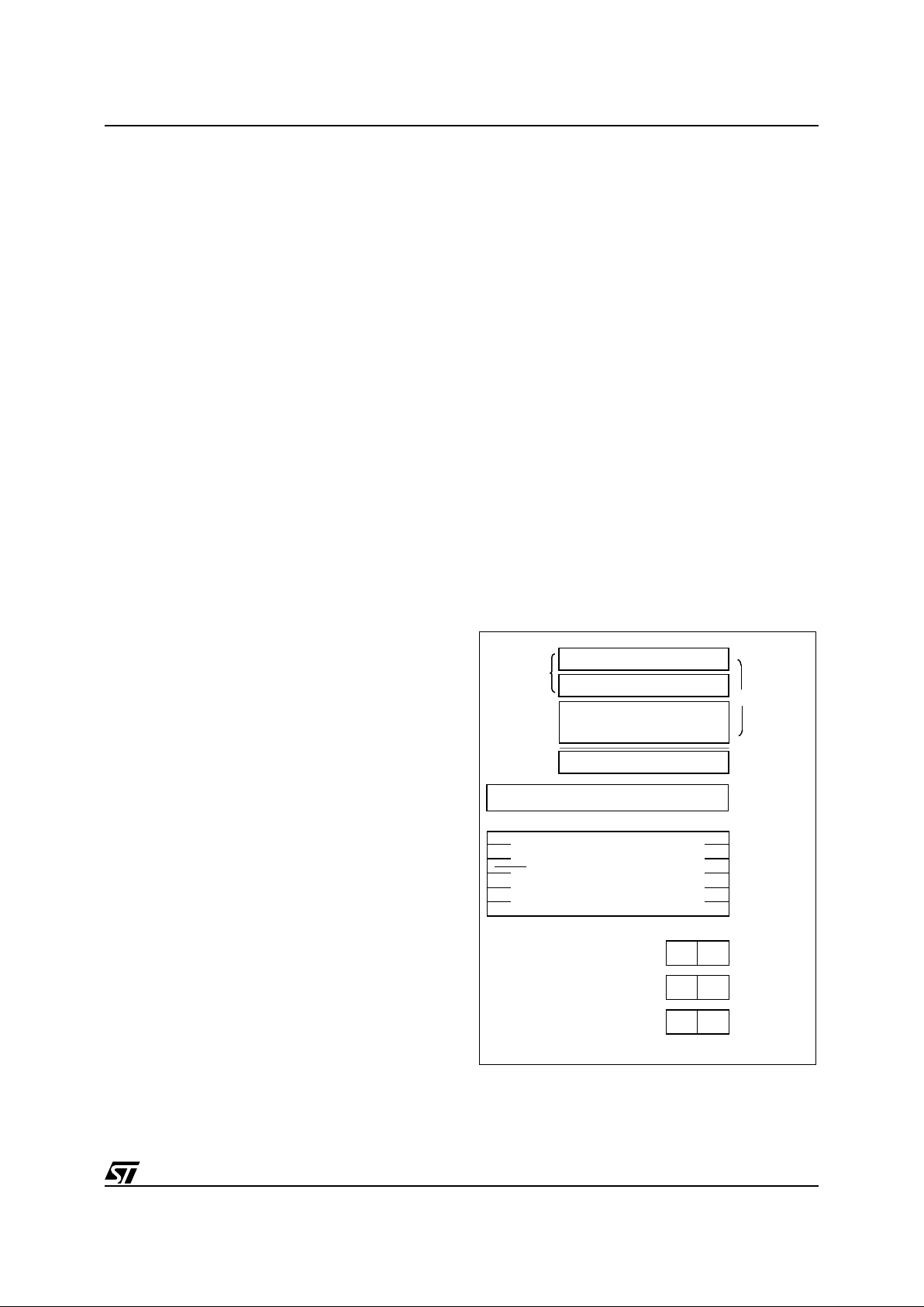
1.4 PROGRAMMING MODES
1.4.1 Option Bytes
The two Option Bytes allow configuration capability to the MCUs. Option byte’s content is automatically read, and the selected options enabled, when
the chip reset is activated.
It can only be accessed during the programming
mode. This access is made either automatically
(copy from a master device) or by selecting the
OPTION BYTE PROGRAMMING mode of the programmer.
The option bytes are located in a non-user m ap.
No address has to be specified.
EPROM Code Option Byte (LSB)
EPROM Code Option Byte (MSB)
D15-D10.
Reserved. Must be cleared
EXTCNTL.
External STOP MODE control.
. When
EXTCNTL is high, STOP mode is available with
watchdog active by setting NMI pin to one.. When
EXTCNTL is low, STOP mode is not available with
the watchdog active.
LVD.
LVD RESET enable.
When this bit is set, safe
RESET is performed by MCU when the supply
voltage is too low. When this bit is cleared, only
power-on reset or external RESET are active.
PROTECT
.
Readout Protection.
This bit allows the
protection of the software contents aga inst p iracy.
When the bit PROTECT is set high, readout of the
OTP contents is prevented by hardware.. When
this bit is low, the user program can be read.
OSCIL
.
Oscillator selection
. When this bit is low,
the oscillator must b e controlled by a quartz crystal, a ceramic resonator or an ex ternal frequenc y.
When it is high, the oscillator must be controlled by
an RC network, with only the resistor having to be
externally provided.
D5.
Reserved. Must be cleared to zero.
D4.
Reserved. Must be set to one.
NMI P U L L.
NMI Pull-Up
. This bit must be set high
to configure the NMI pin with a pull-up resistor.
When it is low, no pull-up is provided
.
TIM PULL .
TIM Pull-Up
. This bit must be set hi gh
to configure the TIME R pi n wi th a pull-up resistor.
When it is low, no pull-up is provided
.
WDACT
. This bit controls the watchdog activation.
When it is high, hardware activation is selected.
The software activation i s sele cted when WDAC T
is low.
OSGEN
.
Oscillator Safe Guard
. This bit must be
set high to enable the Oscillator Safe Guard.
When this bit is low, the OSG is disabled.
The Option byte is writt en duri ng programming either by using the PC menu (PC driven M ode) or
automatically (stand-alone mode)
70
PROTECT
OSCIL - -
NMI
PULL
TIM
PULL
WDACT
OS-
GEN
15 8
------
EXTC-
NTL
LVD
98

11/70
ST62T08C/T09C ST62T10C/T20C /E20C
PROGRA MMING MODES
(Cont’d)
1.4.2 Program Memory
EPROM/OTP programming mode is set by a
+12.5V voltage ap plied to the T EST/V
PP
pin. The
programming flow of the
ST62T08C,T09C,T10C,T20C/E20C is described
in the User Manual of the EPROM Programming
Board.
Table 2. ST62T08C, T09C Program Memory Map
Table 3. ST62T10C Program Memory Map
Table 4. ST62T20C,E20C Program Memory Map
Note
: OTP/EPROM dev ices can be programmed
with the development tools avai lable from STMicroelectro n ics (ST62E2X-EPB o r ST62 2X -KIT).
1.4.3 EPROM Erasing
The EPROM of the windowed package of the
MCUs may be e rased b y exposure to Ultra Violet
light. The erasure characteristic of the MCUs is
such that erasure begins when the memory is exposed to light with a wave lengths shorter than approximately 4000Å. It should be noted that sunlights and some types of fluorescent lam ps have
wavelengths in the range 3000-4000Å.
It is thus recommended that the window of the
MCUs packages be covered by an opaque label to
prevent unintentional erasure problems when testing the application in such an environment.
The recommended erasure procedure of the
MCUs EPROM is the exposure to short w ave ultraviolet light which have a wave-length 2537A.
The integrated dose (i.e. U.V. intensity x exposure
time) for erasure should be a minimum of 30Wsec/cm
2
. The erasure tim e wi th t his do sa ge i s approximately 30 to 40 minutes using an ultraviolet
lamp with 12000µW/cm
2
power rating. The
ST62E20C should be placed within 2.5cm (1Inch)
of the lamp tubes during erasure.
Device Address Descrip tion
0000h-0B9F h
0BA0h-0F9F h
0FA0h-0FEF h
0FF0h-0FF7 h
0FF8h-0FFB h
0FFCh-0FFD h
0FFEh-0FFF h
Reserved
User ROM
Reserved
Interrupt Vectors
Reserved
NMI Interrupt Vector
Reset Vector
Device Address Descrip tion
0000h-087F h
0880h-0F9F h
0FA0h-0FEF h
0FF0h-0FF7 h
0FF8h-0FFB h
0FFCh-0FFD h
0FFEh-0FFF h
Reserved
User ROM
Reserved
Interrupt Vectors
Reserved
NMI Interrupt Vector
Reset Vector
Device Address Description
0000h-007Fh
0080h-0F9Fh
0FA0h-0FEFh
0FF0h-0FF7h
0FF8h-0FFBh
0FFCh-0FFDh
0FFEh-0FFFh
Reserved
User ROM
Reserved
Interrupt Vectors
Reserved
NMI Interrupt Vector
Reset Vector
99

12/70
ST62T08C/T09C ST62T10C/T20C/E20 C
2 CENTRAL PR OCESSING UNIT
2.1 INTRODUCTION
The CPU Core of ST6 devices is independent of the
I/O or Memory conf iguration. As such, it may be
thought of as an independent central processor
communicating with on-chip I/O, Memory and P eripherals via internal address, data, and control
buses. In-core communication is arranged as
shown in Figure 6; the controller being externally
linked to both the Reset and Oscillator circuits,
while the core is linked to the dedicated on-chip peripherals via the serial data bus and indirectly, for
interrupt purposes, through the control registers.
2.2 CPU REGISTERS
The ST6 Family CPU core features six registers and
three pairs of flags available to the programmer.
These are described in the following paragraphs.
Accumulator (A)
. The accumulator is an 8-bit
general purpose register used in all arithmetic calculations, logical operations, and data manipulations. The accumulator can be ad dressed in Data
space as a RAM location at address FFh. Thus the
ST6 can manipulate the accumulator just like any
other register in Data space.
Indirect Registers (X, Y).
These two indirect registers are used as pointers to memory locations in
Data space. They are used in the register-indirect
addressing mode. These registers can be addressed in the data space as RAM locations at addresses 80h (X) and 81h (Y). They can also be accessed with the direct, short direct, or bit direct addressing modes. Accordingly, the ST6 in struction
set can use the indirect registers as any other register of the data space.
Short Direct Registers (V, W).
These two registers are used to save a byte in short direct addressing mode. They can be addressed in Data
space as RAM locations at addresses 82h (V) and
83h (W). They can also be acc ess ed using the direct and bit direct addressing modes. Thus, the
ST6 instruction set can use the short direct registers as any other register of the data space.
Program Counter (PC). The program counter is a
12-bit register which contains the address of the
next ROM location to be processed by the core.
This ROM location may be an opcode, an operand, or the address of an operand. The 12-bit
length allows the direct addressing of 4096 bytes
in Program space.
Figure 6. ST6 Core Block Diagram
PROGRAM
RESET
OPCODE
FLAG
VALUES
2
CONTROLLER
FLAGS
ALU
A-DATA
B-DATA
ADDRESS/READ LINE
DATA SPACE
INTERRUPTS
DATA
RAM/EEPROM
DATA
ROM/EPROM
RESULTS TO DATA SPACE (WRITE LINE)
ROM/EPROM
DEDICATIONS
ACCUMULATOR
CONTROL
SIGNALS
OSCin
OSCout
ADDRESS
DECODER
256
12
Program Counter
and
6 LAYER STACK
0,01 TO 8MHz
VR01811
100
13/70
ST62T08C/T09C ST62T10C/T20C /E20C
CPU REGISTERS
(Cont’d)
However, if the program space contains more than
4096 bytes, the additional memory in program
space can be addressed by using the Program
Bank Switch register.
The PC value is incremented after reading the address of the current instruction. To execute relative
jumps, the PC and the offset are shifted through
the ALU, where they are added; the resul t is then
shifted back into the PC. The program counter can
be changed in the following ways:
- JP (Jump) instructionPC=Jump address
- CALL instructionPC= Call address
- Relative Branch Instruction.PC= PC +/- offset
- Interrupt PC=Interrupt vector
- Reset PC= Reset vector
- RET & RETI instructionsPC= Pop (stack)
- Normal instructionPC= PC + 1
Flags (C, Z)
. The ST6 CPU includes three pairs of
flags (Carry and Zero), each pair being associated
with one of the three normal modes of o peration:
Normal mode, Interrupt mod e and Non Maskable
Interrupt mode. Each pair consists of a CARRY
flag and a ZERO flag. One pa ir (CN, ZN) is used
during Normal operation, another pair is used during Interrupt mode (CI, ZI), and a third pair is used
in the Non Maskable Interrupt mode (CNM I, ZNMI).
The ST6 CPU uses the pair of flags associated
with the current mode: as soon as an interrupt (or
a Non Maskable I nterrupt) is generated, the ST6
CPU uses the Interrupt flags (resp. the NM I flags)
instead of the Normal flags. When the RETI instruction is executed, the previously used set of
flags is restored. It should be noted that each flag
set can only be addressed in its own context (Non
Maskable Interrupt, Normal Interrupt or Main routine). The flags are not cleared during context
switching and thus retain their status.
The Carry flag is set when a carry or a borrow occurs during arithmetic operations; otherwise it is
cleared. The Carry flag is also set to the valu e of
the bit tested in a bit test instruction; it also participates in the rotate left instruction.
The Zero flag is set if the result of the last arithmetic or logical operation was equal to zero; otherwise it is cleared.
Switching between the three sets of flags is performed automatically when an NMI, an interrupt or
a RETI instructions occurs. As the NMI mode is
automatically selected aft er the reset of the MCU,
the ST6 core uses at first the NMI flags.
Stack.
The ST6 CPU in cludes a true LIFO hardware stack which eliminates the need for a stack
pointer. The stack con sists of six sepa rate 12-bit
RAM locations that do not belong to the data
space RAM area. When a subroutine call (or interrupt request) occurs, the contents of each level are
shifted into the next higher level, while the content
of the PC is shifted into the first level (the original
contents of the sixth stack level are lost). When a
subroutine or interrupt return occurs (RET or RETI
instructions), the first level register is shifted back
into the PC and the value of each l evel is popped
back into the previous level. Since the acc umulator, in common with all other data space registers,
is not stored in this stack, management of these
registers should be performed within the subroutine. The stack will remain in its “deepest” position
if more than 6 nested calls or interrupts are executed, and consequent ly the last return address wi ll
be lost. It will al so remain in its highest position if
the stack is empty and a RET or RETI is executed.
In this case the next instruction will be executed.
Figure 7. ST6 CP U Pr ogramming Mode
l
SHORT
DIRECT
ADDRESSING
MODE
VREGISTER
WREGISTER
PROGRAMCOUNTER
SIX LEVELS
STACK REGISTER
CZNORMAL FLAGS
INTERRUPT FLAGS
NMI FL AGS
INDEX
REGISTER
VA 000 42 3
b7
b7
b7
b7
b7
b0
b0
b0
b0
b0
b0b11
ACCUMULATOR
YREG.POINTER
XREG.POINTER
CZ
CZ
101
14/70
ST62T08C/T09C ST62T10C/T20C/E20 C
3 CLOCKS, RESET, INTER RUPTS AND POWER SAV ING MODES
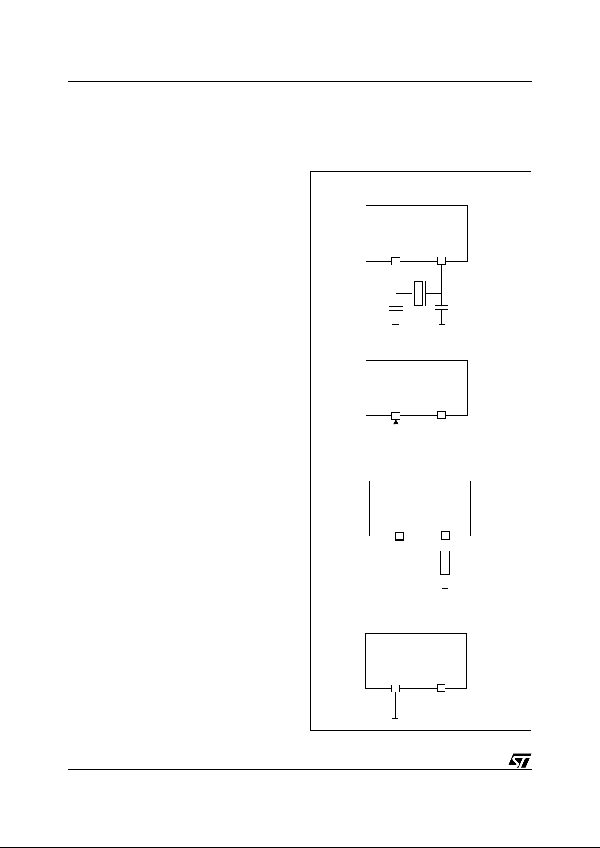
3.1 CLOCK SYSTEM
The MCU f e atures a Main Oscillator w hic h c an be
driven by an external clock, or used in conjunction
with an AT-cut parallel resonant crystal or a s uitable ceramic resonator, or with an external resistor
(R
NET
). In addition, a Low Frequency Auxiliary Oscillator (LFAO) can be switched in for security reasons, to reduce power consumption, or to offer the
benefits of a back-up clock system.
The Oscillator Safeguard (OSG) option filters
spikes from the oscillator lines, provides access to
the LFAO to provide a backup oscillator in the
event of main oscillator failure and also automatically limits the internal cloc k frequency (f
INT
) as a
function of V
DD
, in order to guarantee correct operation. The se functions a re illustrated in Figure 9,
Figure 10, Figure 11 and Figure 12.
Figure 8 illustrates var i o us po ssible oscilla t or co n -
figurations using an external crystal or ceramic resonator, an external clock input, an external resistor
(R
NET
), or the lowest cost solution using only the
LFAO. C
L1
an CL2 should have a capacitance in the
range 12 to 22 pF for an oscillator frequency in the
4-8 MHz range.
The internal MCU clock frequency (f
INT
) is divided
by 12 to drive the Timer, the A/D converter and the
Watchdog timer, and by 13 to drive the CPU core,
as may be seen in Figure 11.
With an 8MHz oscillator frequency, the fastest machine cycle is therefore 1.625µs.
A machine cycle is the smallest unit of time needed
to execute any operation (for instance, to increment
the Program Counter). An i nstruction may requi re
two, four, or five machine cycles for execution.
3.1.1 Main Oscillator
The oscillator configuration may be specified by selecting the appropriate option. When the CRYSTAL/
RESONATOR option is selected, it must be used with
a quartz crystal, a ceramic resonator or an external
signal provided on the OSCin pin. When the RC NETWORK option is selected, the system clock is generated by an external resistor.
The main oscillator can be turned off (when the
OSG ENABLED option is selec ted) by setting the
OSCOFF bit of the ADC Control Register. The
Low Frequency Auxiliary Oscillator is automatically started.
Figure 8. Oscillator Configurations
INTEGRATED CL OCK
CRYSTAL/RESONATOR option
OSG ENABLED option
OSC
in
OSC
out
C
L1n
C
L2
ST6xxx
CRYSTAL/RESONATO R CLOCK
CRYSTAL/RESONATOR option
OSC
in
OSC
out
ST6xxx
EXTERNAL CLOCK
CRYSTAL/RESONATOR option
NC
OSC
in
OSC
out
ST6xxx
NC
OSC
in
OSC
out
R
NET
ST6xxx
RC NETWORK
RC NETW O RK option
NC
102

15/70
ST62T08C/T09C ST62T10C/T20C /E20C
CLOCK SYSTEM
(Cont’d)
Turning on the main oscillator is achieved by resetting the OSCOFF bit of the A/D Converter Control Register or by resetting the MCU. Restarting
the main osc illator im plies a dela y comp rising the
oscillator start up delay period plus the duration of
the software instruction at f
LFAO
clock frequency.
3.1.2 Low Frequency Auxiliary Oscillator
(LFAO)
The Low Frequency Auxiliary Oscillator has three
main purposes. Firstly, it can be used t o reduce
power consumption in non timing critical routines.
Secondly, it offers a fully integrated system clock,
without any external components. Lastly, it acts as
a safety oscillator in case of main oscillator failure.
This oscillator is available when the OSG ENABLED option is selected. In this case, it automatically starts one of its periods after the first missing
edge from the main oscillator, whatever the reason
(main oscillator defective, no clock circuitry provided, main osc illator switched off...).
User code, normal interrupts, WAIT and STOP instructions, are processed as normal, at the reduced f
LFAO
frequency. The A/D converter accuracy is decreased, since the internal frequency is below 1MHz.
At power on, the Low Frequency Aux ilia ry Osc ill ator starts faster than the Main Oscillator. It therefore feeds the on-chip counter generating the POR
delay until the Main Oscillator runs.
The Low Frequency Auxiliary Oscillator is automatically switched off as soon as the main oscillator sta r ts.
ADCR
Address: 0D1h — Read/Write
Bit 7-3, 1-0=
ADCR7-ADCR3, ADCR1-ADCR0
:
ADC Control Register
.
These bits are not used.
Bit 2 =
OSCOFF
. When low, this bit enables m ain
oscillator to run. The main oscillator is switc hed off
when OSCOFF is high.
3.1.3 Oscillator Safe Guard
The Oscillator Safe Guard (OSG) affords drastically increased operational integrity in S T62xx dev ices. The OSG circuit provides three basic functions: it filters spikes from the oscillator lines which
would result in over frequency to the ST62 CPU; it
gives access to the Low Freque ncy Auxiliary Oscillator (L FA O), used to ens u re m in im u m processing in case of main oscillator failure, to offer reduced power consumption or to provide a fixed frequency low cost oscillator; finally, it automatically
limits the internal clock frequency as a f unction of
supply voltage, in order to ensure correct operation even if the power supply should drop.
The OSG is enabled or disabled by choosing the
relevant OSG option. It may b e viewed as a filter
whose cross-over frequency is device dependent.
Spikes on the oscillator lines result in an effectively
increased internal clock frequency. In the absence
of an OSG circuit, this may lead to an over frequency for a given power supply voltage. The
OSG filters out such spikes (as illustrated in Figure
9). In all cases, when the OSG is active, the maxi-
mum internal clock frequency, f
INT
, is limited to
f
OSG
, which is supply voltage depende nt. This re-
lationship is illustrated in Figure 12.
When the OSG is enabled, the Low Frequency
Auxiliary Oscillator may be accessed. This oscillator starts operating after the first missing edge of
the main oscillator (see Figure 10).
Over-frequency, at a given power supp ly level, is
seen by the OSG as spikes; it therefore filte rs out
some cycles in order that the internal clock frequency of the device is kept within the range the
particular device can stand (depen ding on V
DD
),
and below f
OSG
: the maximum authorised frequen-
cy with OSG enabled.
Note.
The OSG should be used wherever possible
as it provides maximum safet y. Care must be taken, however, as it ca n increase power consumption and reduce the maximum operating frequency
to f
OSG
.
70
ADCR7ADCR6ADCR5ADCR4ADCR3OSC
OFF
ADCR1ADCR
0
103
16/70
ST62T08C/T09C ST62T10C/T20C/E20 C
CLOCK SYSTEM
(Cont’d)
Figure 9. OSG Filtering Principle
Figure 10. OSG Emergency Oscillator Principle
(1)
VR001932
(3)
(2)
(4)
(1)
(2)
(3)
(4)
Maximum Frequency for the device to work correctly
Actual Quartz Crystal Frequency at OSCin pin
Noise from OSCin
Resulting Internal Frequency
Main
VR001933
Internal
Emergency
Oscillator
Frequency
Oscillator
104
17/70
ST62T08C/T09C ST62T10C/T20C /E20C
CLOCK SYSTEM
(Cont’d)
Figure 11. Clock Circuit Block Diagram
Figure 12. Maximum Operating Frequency (f
MAX
) versus Supply Voltage (VDD)
Notes
:
1. In this area, operation is guaranteed at the
quartz crystal frequency.
2. When the OSG is disabled, operation in this
area is guaranteed at the crystal frequency. When
the OSG is enabled, operation in this area is guaranteed at a frequency of at least f
OSG Min.
3. When the OSG is disabled, operation in this
area is guaranteed at the quartz crystal frequency.
When the OSG is enab led, access to this a rea is
prevented. The internal frequency is kept a f
OSG.
4. When the OSG is disabled, operation in this
area is not guaranteed
When the OSG is enab led, access to this a rea is
prevented. The internal frequency is kept at f
OSG.
MAIN
OSCILLATOR
OSG
LFAO
M
U
X
Core
:
13
:
12
:
1
TIMER 1
Watchdog
POR
f
INT
Main Oscillator off
1
2.5
3.644.555.56
8
7
6
5
4
3
2
Maximum FREQUENCY (MHz)
SUPPLY VOLTAGE (V
DD
)
FUNCTIONALITY IS NOT
3
4
3
2
1
f
OSG
f
OSG
Min
GUARANTEED
IN THIS AREA
VR01807
105
18/70
ST62T08C/T09C ST62T10C/T20C/E20 C
3.2 RESETS
The MCU can be reset in four ways:
– by the external Reset input being pulled low;
– by Power-on Reset;
– by the digital Watchdog peripheral timing out.
– by Low Voltage Detection (LVD)
3.2.1 RESET Input
The RESET
pin may be connected to a device of
the application board in order to reset the MCU if
required. The RESET
pin may be pulled low in
RUN, WAIT or STOP mode. This input can be
used to reset the MCU internal state and ensure a
correct start-up procedure. The pin is active low
and features a Schmitt trigger input. The internal
Reset signal is generated by adding a delay to the
external signal. Therefore even short pulses on
the RESET
pin are acceptable, provide d VDD has
completed its rising phase and that the oscillator is
running correctly (normal RUN or WAIT modes).
The MCU is kept in the Reset state as long as the
RESET
pin is held low.
If RESET
activation occurs in the RUN or WAIT
modes, processing of the user program is stopped
(RUN mode only), the Inputs and Outputs are configured as inputs with pull-up resistors and the
main Oscillator is restarted. When the level on the
RESET pin then goes high, the initialization sequence is executed following expiry of the internal
delay period.
If RESET
pin activation occurs in the STOP mode,
the oscillator starts up and all Inputs and Outputs
are configured as inputs with pull-up resistors.
When the level of the RESET
pin then goes high,
the initialization sequence is executed following
expiry of the internal delay period.
3.2.2 Power-on Reset
The function of the POR circuit cons ists in waking
up the MCU by detecting around 2V a dynamic
(rising edge) variation of the VDD Supply. At the
beginning of this sequence, the MCU is configured
in the Reset state: al l I/O ports are c onfigured as
inputs with pull-up resistors an d no instruction is
executed. When the power supply voltage rises to
a sufficient level, the os cillator starts to operate,
whereupon an internal delay is initiated, in order to
allow the oscillator to fully s tabil ize b efore execut ing the first instruction. The initialization sequence
is executed immediately following the internal delay.
To ensure correct start-up, the user should take
care that the VDD Supply is stabilized at a sufficient level for the chosen frequency (see recommended operation) before the reset signal is released. In addition, supply rising must start from
0V.
As a consequence, the POR does not allow to supervise static, slowly rising, or falling, or noisy
(present in g o s c illation) VDD supplies.
An external RC network connected to the RESET
pin, or the LVD reset can b e used instead to get
the best performances.
Figure 13. Reset and Interrupt Processing
INT LATCH CLEARED
NMI M ASK SET
RESET
( IF PRESENT )
SELECT
NMI MODE FLAGS
IS RESET STILL
PRESENT?
YES
PUT FFEH
ON ADDRESS BUS
FROM RESET LOCATIONS
FFE/FFF
NO
FETCH INSTRUCTION
LOAD PC
VA000427
106
19/70
ST62T08C/T09C ST62T10C/T20C /E20C
RESETS
(Cont’d)
3.2.3 Watchdog Reset
The MCU provides a Wat chdog timer function in
order to ensure graceful recovery from software
upsets. If the Watchdog regi ster is not refreshed
before an end-of-count condition is reached, the
internal reset will be activated. This, amongs t ot her things, resets the watchdog counter.
The MCU restarts just as though the Reset had
been generated by the RESET
pin, including the
built-in stabilisation delay period .
3.2.4 LVD Reset
The on-chip Low Voltage Detector, selectable as
user option, features static Reset when supply
voltage is below a reference value. Thanks to this
feature, external reset circuit can be removed
while keeping the application safety. This SAFE
RESET is effective as well in Power-on phase as
in power supply drop with different reference val-
ues, allowing hysteresis effect. Reference value in
case of voltage drop has been set lower than the
reference value for power-on in order to avoid any
parasitic Reset when MCU start's running and
sinking current on the supply.
As long as the supply voltage is below the reference value, there is a internal and static RESET
command. The MCU can start only when the supply voltage rises over the reference value. Therefore, only two operating mode exist for the MCU:
RESET active below the voltage reference, and
running mode over the voltage reference as
shown on the Figur e 14, that represents a powerup, power-down sequence.
Note
: When the RESET state is controlled by one
of the internal RESET sources (Low Voltage Detector, Watchdog, Power on Reset), the RESET
pin is tied to low logic level.
Figure 14. LVD Reset on Power-on and Power-down (Brown -out)
3.2.5 Application Notes
No external resistor is requi red betw een V
DD
and
the Reset pin, thanks to the built-in pull-up device.
Direct external connection of the pin RESET to
V
DD
must be avoided in order to ensure safe behaviour of the internal reset sources (AND.Wired
structure).
RESET
RESET
VR02 106 A
time
V
Up
V
dn
V
DD
107
20/70
ST62T08C/T09C ST62T10C/T20C/E20 C
RESETS
(Cont’d)
3.2.6 MCU Initialization Sequence
When a reset occurs the stack is reset, the PC is
loaded with the address of the Reset Vector (located in program ROM starting at address 0FFEh). A
jump to the beginning of the user program must be
coded at this address. Following a Reset, the I nterrupt flag is automatically set, so that the CPU is
in Non Maskable Interrupt mode; this prevents the
initialisation routine from being interrupted. The initialisation routine should therefore be terminated
by a RETI instruction, in order to revert to normal
mode and enable interrupts. If no pending interrupt
is present at the end of the initialisation routine, the
MCU will continue by processing the instruction
immediately following the RETI instruction. If, however, a pending interrupt is present, it will be serviced.
Figure 15. Reset and Interrupt Processing
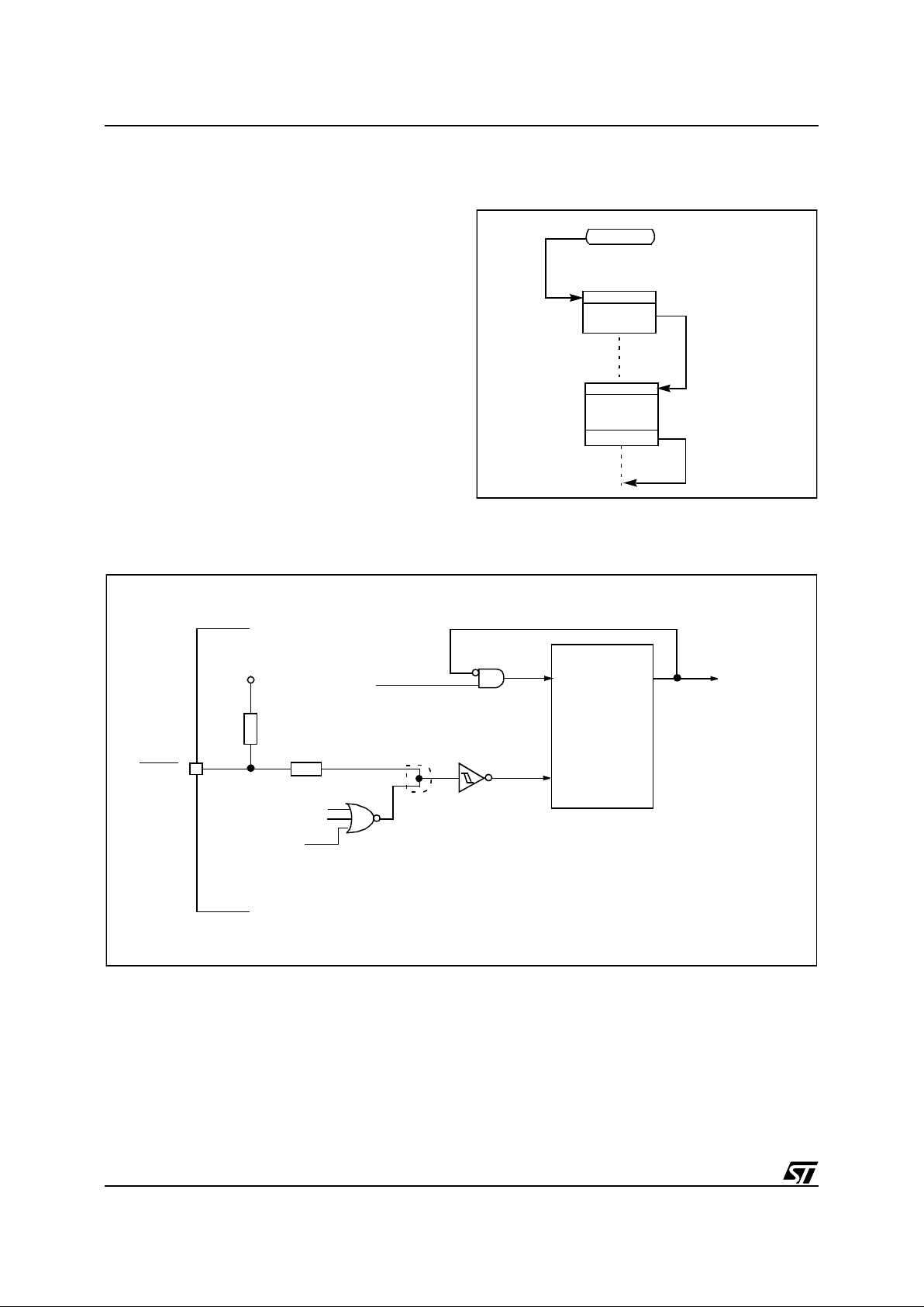
Figure 16. Reset Block Diagram
RESET
RESET
VECTOR
JP
JP:2 BYTES/4 CYCLES
RETI
RETI: 1 BYTE/2 CYCLES
INITIALIZATION
ROUTINE
VA00181
V
DD
RESET
R
PU
R
ESD
1)
POWER
WATCHDOG RESET
CK
COUNTER
RESET
ST6
INTERNAL
RESET
f
OSC
RESET
ON RESET
LVD RESE T
VR02107A
AND. Wired
1) Resis t i ve E SD protect io n. Value not guaranteed.
108

21/70
ST62T08C/T09C ST62T10C/T20C /E20C
RESETS
(Cont’d)
Table 5. Register Reset Status
Register Address(es) Status Comment
Oscillator Control Register
Port Data Registers
Port Direction Register
Port Option Register
Interrupt Option Register
TIMER Status/Control
0DCh
0C0h to 0C1h
0C4h to 0C5h
0CCh to 0CDh
0C8h
0D4h
00h
f
INT
= f
OSC
; OSG disabled
I/O are Input with pull-up
I/O are Input with pull-up
I/O are Input with pull-up
Interrupt disabled
TIMER disabled
X, Y, V, W, Register
Accumulator
Data RAM
Data ROM Window Register
A/D Result Register
080H TO 083H
0FFh
084h to 0BFh
0C9h
0D0h
Undefined As written if programmed
TIMER Counter Register
TIMER Prescaler Register
Watchdog Counter Register
A/D Control Register
0D3h
0D2h
0D8h
0D1h
FFh
7Fh
FEh
40h
Max count loaded
A/D in Standby (When available)
109
 Loading...