


SGS Thomson Microelectronics ST72F623F2T1, ST72F623F2M1, ST72F623F2B1, ST72F623, ST72P622K2M1 Datasheet
...ST7262
LOW SPEED USB 8-BIT MCU WITH 3 ENDPOINTS, FLASH OR ROM MEMORY, LVD, WDG, 10-BIT ADC, 2 TIMERS, SCI, SPI
■Memories
–8K or 16K Program memory
(ROM, FASTROM or Dual voltage FLASH) with read-write protection
–In-Application and In-Circuit Programming for FLASH versions
–384 to 768 bytes RAM (128-byte stack)
■Clock, Reset and Supply Management
–Enhanced Reset System (Power On Reset)
–Low Voltage Detector (LVD)
–Clock-out capability
–6 or 12 MHz Oscillator (8, 4, 2, 1 MHz internal frequencies)
–3 Power saving modes
■USB (Universal Serial Bus) Interface
–DMA for low speed applications compliant with USB 1.5 Mbs specification (v 1.1) and USB HID specification (v 1.0):
–Integrated 3.3V voltage regulator and transceivers
–Suspend and Resume operations
–3 Endpoints
■Up to 31 I/O Ports
–Up to 31 multifunctional bidirectional I/O lines
–Up to 12 External interrupts (3 vectors)
–13 alternate function lines
–8 high sink outputs
(8 mA@0.4 V/20 mA@1.3 V)
–2 true open drain pins (N buffer 8 mA@0.4 V)
■3 Timers
–Configurable watchdog timer (8 to 500 ms timeout)
–8-bit Auto Reload Timer (ART) with 2 Input Captures, 2 PWM outputs and External Clock
–8-bit Time Base Unit (TBU) for generating periodic interrupts cascadable with ART
Device Summary
SO20 |
PDIP20 |
SO34 shrink |
PDIP32 shrink |
TQFP44 |
PDIP42 shrink |
■Analog Peripheral
–10-bit A/D Converter with up to 8 input pins.
■2 Communications Interfaces
–Asynchronous Serial Communication interface
–Synchronous Serial Peripheral Interface
■Instruction Set
–8-bit data manipulation
–63 basic instructions
–17 main addressing modes
–8 x 8 unsigned multiply instruction
–True bit manipulation
■Nested interrupts
■Development Tools
–Full hardware/software development package
Features |
ST72623F2 |
ST72622K2 |
|
ST72621K4 |
ST72622L2 |
|
ST72621L4 |
ST72621J2 |
|
ST72621J4 |
|
|
|
|
|
|
|
|
|
|
|
Program memory - bytes |
8K |
8K |
|
16K |
8K |
|
16K |
8K |
|
16K |
|
|
|
|
|
|
|
|
|
|
|
RAM (stack) - bytes |
384 (128) |
384 (128) |
|
768 (128) |
384 (128) |
|
768 (128) |
384 (128) |
|
768 (128) |
|
|
|
|
|
|
|
|
|||
Peripherals |
USB, |
Watchdog, Low |
Voltage Detector, |
8-bit Auto-Reload timer, Timebase unit, A/D Converter |
||||||
|
|
|
|
|
|
|
|
|
|
|
Serial I/O |
- |
SPI |
|
SPI + SCI |
SPI |
|
|
SPI + SCI |
|
|
|
|
|
|
|
|
|
|
|
|
|
I/Os |
11 |
|
21 |
|
23 |
|
31 |
|||
|
|
|
|
|
|
|
|
|||
Operating Supply |
|
4.0V to 5.5V (Low voltage |
3.0V to 5.5V ROM versions available) |
|
|
|||||
|
|
|
|
|
|
|
|
|
|
|
Operating Temperature |
|
|
|
|
0°C to +70°C |
|
|
|
|
|
|
|
|
|
|
|
|
|
|||
Packages |
PDIP20/SO20 |
PDIP32 |
SO34 |
PDIP42/TQFP44 |
||||||
|
|
|
|
|
|
|
|
|
|
|
|
Rev. 2.2 |
June 2003 |
1/132 |
|
|
|
1 |

Table of Contents
1 INTRODUCTION . . . . . . . . . . . . . . . . . . . . . . . . . . . . . . . . . . . . . . . . . . . . . . . . . . . . . . . . . . . . . . 4 2 PIN DESCRIPTION . . . . . . . . . . . . . . . . . . . . . . . . . . . . . . . . . . . . . . . . . . . . . . . . . . . . . . . . . . . . 5
2.1 PCB LAYOUT RECOMMENDATION . . . . . . . . . . . . . . . . . . . . . . . . . . . . . . . . . . . . . . . . . 10
3 REGISTER & MEMORY MAP . . . . . . . . . . . . . . . . . . . . . . . . . . . . . . . . . . . . . . . . . . . . . . . . . . . |
1 1 |
4 FLASH PROGRAM MEMORY . . . . . . . . . . . . . . . . . . . . . . . . . . . . . . . . . . . . . . . . . . . . . . . . . . |
14 |
4.1 INTRODUCTION . . . . . . . . . . . . . . . . . . . . . . . . . . . . . . . . . . . . . . . . . . . . . . . . . . . . . . . . 14 4.2 MAIN FEATURES . . . . . . . . . . . . . . . . . . . . . . . . . . . . . . . . . . . . . . . . . . . . . . . . . . . . . . . 14 4.3 STRUCTURE . . . . . . . . . . . . . . . . . . . . . . . . . . . . . . . . . . . . . . . . . . . . . . . . . . . . . . . . . . . 14 4.4 ICC INTERFACE . . . . . . . . . . . . . . . . . . . . . . . . . . . . . . . . . . . . . . . . . . . . . . . . . . . . . . . . 15 4.5 ICP (IN-CIRCUIT PROGRAMMING) . . . . . . . . . . . . . . . . . . . . . . . . . . . . . . . . . . . . . . . . . 16 4.6 IAP (IN-APPLICATION PROGRAMMING) . . . . . . . . . . . . . . . . . . . . . . . . . . . . . . . . . . . . . 16 4.7 RELATED DOCUMENTATION . . . . . . . . . . . . . . . . . . . . . . . . . . . . . . . . . . . . . . . . . . . . . 16 4.8 REGISTER DESCRIPTION . . . . . . . . . . . . . . . . . . . . . . . . . . . . . . . . . . . . . . . . . . . . . . . . 16
5 CENTRAL PROCESSING UNIT . . . . . . . . . . . . . . . . . . . . . . . . . . . . . . . . . . . . . . . . . . . . . . . . . |
17 |
|
5.1 |
INTRODUCTION . . . . . . . . . . . . . . . . . . . . . . . . . . . . . . . . . . . . . . . . . . . . . . . . . . . . . . . . |
17 |
5.2 |
MAIN FEATURES . . . . . . . . . . . . . . . . . . . . . . . . . . . . . . . . . . . . . . . . . . . . . . . . . . . . . . . |
17 |
5.3 |
CPU REGISTERS . . . . . . . . . . . . . . . . . . . . . . . . . . . . . . . . . . . . . . . . . . . . . . . . . . . . . . . |
17 |
6 CLOCKS AND RESET . . . . . . . . . . . . . . . . . . . . . . . . . . . . . . . . . . . . . . . . . . . . . . . . . . . . . . . . |
20 |
|
6.1 |
CLOCK SYSTEM . . . . . . . . . . . . . . . . . . . . . . . . . . . . . . . . . . . . . . . . . . . . . . . . . . . . . . . . |
20 |
6.2 |
RESET . . . . . . . . . . . . . . . . . . . . . . . . . . . . . . . . . . . . . . . . . . . . . . . . . . . . . . . . . . . . . . . . |
21 |
7 INTERRUPTS . . . . . . . . . . . . . . . . . . . . . . . . . . . . . . . . . . . . . . . . . . . . . . . . . . . . . . . . . . . . . . . |
23 |
|
7.1 INTRODUCTION . . . . . . . . . . . . . . . . . . . . . . . . . . . . . . . . . . . . . . . . . . . . . . . . . . . . . . . . 23 7.2 MASKING AND PROCESSING FLOW . . . . . . . . . . . . . . . . . . . . . . . . . . . . . . . . . . . . . . . 23 7.3 INTERRUPTS AND LOW POWER MODES . . . . . . . . . . . . . . . . . . . . . . . . . . . . . . . . . . . 25 7.4 CONCURRENT & NESTED MANAGEMENT . . . . . . . . . . . . . . . . . . . . . . . . . . . . . . . . . . 25 7.5 INTERRUPT REGISTER DESCRIPTION . . . . . . . . . . . . . . . . . . . . . . . . . . . . . . . . . . . . . 26 7.6 INTERRUPT REGISTER . . . . . . . . . . . . . . . . . . . . . . . . . . . . . . . . . . . . . . . . . . . . . . . . . . 27
8 POWER SAVING MODES . . . . . . . . . . . . . . . . . . . . . . . . . . . . . . . . . . . . . . . . . . . . . . . . . . . . . |
29 |
8.1 INTRODUCTION . . . . . . . . . . . . . . . . . . . . . . . . . . . . . . . . . . . . . . . . . . . . . . . . . . . . . . . . 29 8.2 WAIT MODE . . . . . . . . . . . . . . . . . . . . . . . . . . . . . . . . . . . . . . . . . . . . . . . . . . . . . . . . . . . 29 8.3 HALT MODE . . . . . . . . . . . . . . . . . . . . . . . . . . . . . . . . . . . . . . . . . . . . . . . . . . . . . . . . . . . 30
9 I/O PORTS . . . . . . . . . . . . . . . . . . . . . . . . . . . . . . . . . . . . . . . . . . . . . . . . . . . . . . . . . . . . . . . . . . 31
9.1 INTRODUCTION . . . . . . . . . . . . . . . . . . . . . . . . . . . . . . . . . . . . . . . . . . . . . . . . . . . . . . . . 31 9.2 FUNCTIONAL DESCRIPTION . . . . . . . . . . . . . . . . . . . . . . . . . . . . . . . . . . . . . . . . . . . . . . 31 9.3 MISCELLANEOUS REGISTER . . . . . . . . . . . . . . . . . . . . . . . . . . . . . . . . . . . . . . . . . . . . . 39
10 ON-CHIP PERIPHERALS . . . . . . . . . . . . . . . . . . . . . . . . . . . . . . . . . . . . . . . . . . . . . . . . . . . . . |
40 |
10.1 WATCHDOG TIMER (WDG) . . . . . . . . . . . . . . . . . . . . . . . . . . . . . . . . . . . . . . . . . . . . . . . 40 10.2 PWM AUTO-RELOAD TIMER (ART) . . . . . . . . . . . . . . . . . . . . . . . . . . . . . . . . . . . . . . . . . 42 10.3 TIMEBASE UNIT (TBU) . . . . . . . . . . . . . . . . . . . . . . . . . . . . . . . . . . . . . . . . . . . . . . . . . . . 5 2 10.4 SERIAL PERIPHERAL INTERFACE (SPI) . . . . . . . . . . . . . . . . . . . . . . . . . . . . . . . . . . . . 55 10.5 SERIAL COMMUNICATIONS INTERFACE (SCI) . . . . . . . . . . . . . . . . . . . . . . . . . . . . . . . 66
2/132
1

Table of Contents
10.6 USB INTERFACE (USB) . . . . . . . . . . . . . . . . . . . . . . . . . . . . . . . . . . . . . . . . . . . . . . . . . . 80 10.7 10-BIT A/D CONVERTER (ADC) . . . . . . . . . . . . . . . . . . . . . . . . . . . . . . . . . . . . . . . . . . . . 88
11 INSTRUCTION SET . . . . . . . . . . . . . . . . . . . . . . . . . . . . . . . . . . . . . . . . . . . . . . . . . . . . . . . . |
. 92 |
11.1 CPU ADDRESSING MODES . . . . . . . . . . . . . . . . . . . . . . . . . . . . . . . . . . . . . . . . . . . . . . |
. 92 |
11.2 INSTRUCTION GROUPS . . . . . . . . . . . . . . . . . . . . . . . . . . . . . . . . . . . . . . . . . . . . . . . . |
. 95 |
12 ELECTRICAL CHARACTERISTICS . . . . . . . . . . . . . . . . . . . . . . . . . . . . . . . . . . . . . . . . . . . . . |
98 |
12.1 PARAMETER CONDITIONS . . . . . . . . . . . . . . . . . . . . . . . . . . . . . . . . . . . . . . . . . . . . . . . |
98 |
12.2 ABSOLUTE MAXIMUM RATINGS . . . . . . . . . . . . . . . . . . . . . . . . . . . . . . . . . . . . . . . . . . . |
99 |
12.3 OPERATING CONDITIONS . . . . . . . . . . . . . . . . . . . . . . . . . . . . . . . . . . . . . . . . . . . . . . . |
100 |
12.4 SUPPLY CURRENT CHARACTERISTICS . . . . . . . . . . . . . . . . . . . . . . . . . . . . . . . . . . . |
102 |
12.5 CLOCK AND TIMING CHARACTERISTICS . . . . . . . . . . . . . . . . . . . . . . . . . . . . . . . . . . |
103 |
12.6 MEMORY CHARACTERISTICS . . . . . . . . . . . . . . . . . . . . . . . . . . . . . . . . . . . . . . . . . . . |
105 |
12.7 EMC CHARACTERISTICS . . . . . . . . . . . . . . . . . . . . . . . . . . . . . . . . . . . . . . . . . . . . . . . |
106 |
12.8 I/O PORT PIN CHARACTERISTICS . . . . . . . . . . . . . . . . . . . . . . . . . . . . . . . . . . . . . . . . |
111 |
12.9 CONTROL PIN CHARACTERISTICS . . . . . . . . . . . . . . . . . . . . . . . . . . . . . . . . . . . . . . . |
114 |
12.10TIMER PERIPHERAL CHARACTERISTICS . . . . . . . . . . . . . . . . . . . . . . . . . . . . . . . . . |
116 |
12.11COMMUNICATION INTERFACE CHARACTERISTICS . . . . . . . . . . . . . . . . . . . . . . . . |
117 |
12.1210-BIT ADC CHARACTERISTICS . . . . . . . . . . . . . . . . . . . . . . . . . . . . . . . . . . . . . . . . . |
120 |
13 PACKAGE CHARACTERISTICS . . . . . . . . . . . . . . . . . . . . . . . . . . . . . . . . . . . . . . . . . . . . . . |
123 |
13.1 PACKAGE MECHANICAL DATA . . . . . . . . . . . . . . . . . . . . . . . . . . . . . . . . . . . . . . . . . . . |
123 |
14 DEVICE CONFIGURATION AND ORDERING INFORMATION . . . . . . . . . . . . . . . . . . . . . . . |
126 |
14.1 OPTION BYTE . . . . . . . . . . . . . . . . . . . . . . . . . . . . . . . . . . . . . . . . . . . . . . . . . . . . . . . . . |
126 |
14.2 DEVICE ORDERING INFORMATION AND TRANSFER OF CUSTOMER CODE . . . . . 126 |
|
14.3 DEVELOPMENT TOOLS . . . . . . . . . . . . . . . . . . . . . . . . . . . . . . . . . . . . . . . . . . . . . . . . . |
128 |
15 IMPORTANT NOTES . . . . . . . . . . . . . . . . . . . . . . . . . . . . . . . . . . . . . . . . . . . . . . . . . . . . . . . |
130 |
15.1 UNEXPECTED RESET FETCH . . . . . . . . . . . . . . . . . . . . . . . . . . . . . . . . . . . . . . . . . . . . |
130 |
15.2 HALT MODE POWER CONSUMPTION WITH ADC ON . . . . . . . . . . . . . . . . . . . . . . . . . |
130 |
16 SUMMARY OF CHANGES . . . . . . . . . . . . . . . . . . . . . . . . . . . . . . . . . . . . . . . . . . . . . . . . . . . |
131 |
To obtain the most recent version of this datasheet,
please check at www.st.com>products>technical literature>datasheet
Please pay special attention to the Section “IMPORTANT NOTES” on page 130.
3/132
ST7262
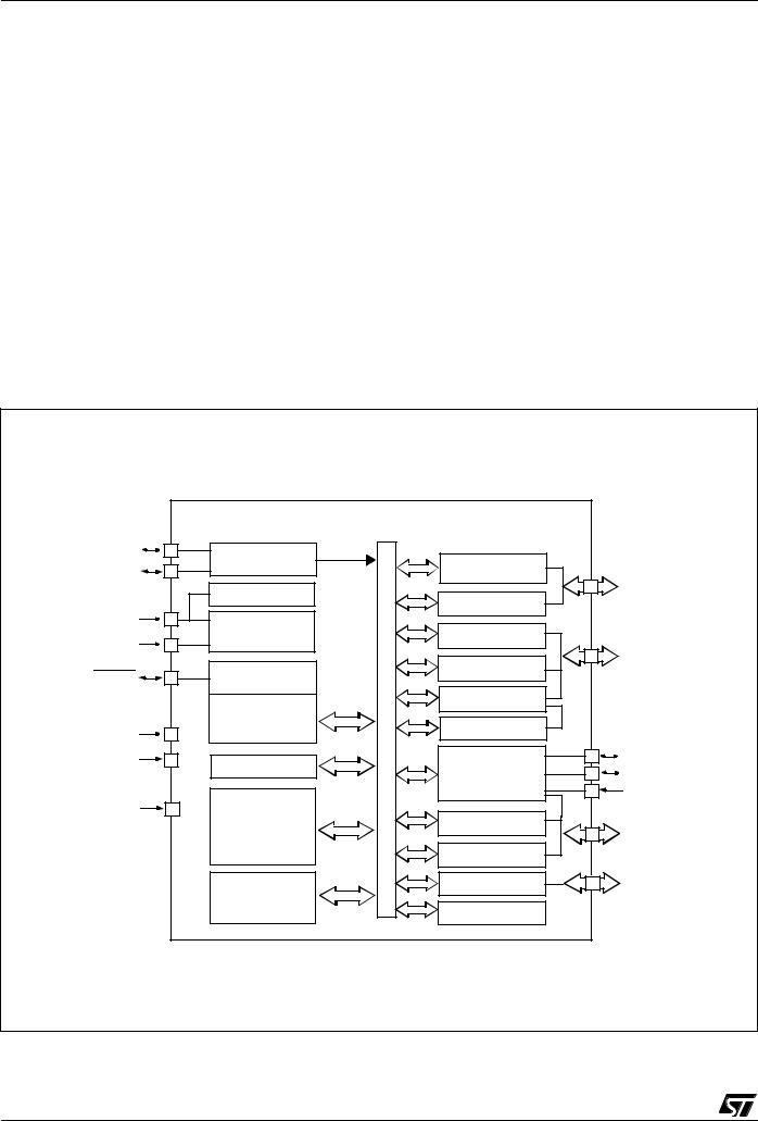
1 INTRODUCTION
The ST7262, ST72P62 and ST72F62 devices are members of the ST7 microcontroller family designed for USB applications.
All devices are based on a common industrystandard 8-bit core, featuring an enhanced instruction set.
The ST7262 devices are ROM versions.
The ST72P62 devices are Factory Advanced Service Technique ROM (FASTROM) versions: they are factory-programmed and are not reprogrammable.
The ST72F62 versions feature dual-voltage FLASH memory with FLASH Programming capability.
Figure 1. General Block Diagram
Under software control, all devices can be placed in WAIT, SLOW, or HALT mode, reducing power consumption when the application is in idle or standby state.
The enhanced instruction set and addressing modes of the ST7 offer both power and flexibility to software developers, enabling the design of highly efficient and compact application code. In addition to standard 8-bit data management, all ST7 microcontrollers feature true bit manipulation, 8x8 unsigned multiplication and indirect addressing modes.
|
|
Internal |
|
OSCIN |
OSCILLATOR |
CLOCK |
|
OSCOUT |
10-BIT ADC |
|
|
|
|
||
|
LVD |
|
PA7:0 |
|
PORT A |
(8 bits) |
|
VDD |
|
||
|
|
||
POWER |
|
|
|
VSS |
SUPPLY |
SCI |
|
|
|
PB7:0 |
|
|
|
PORT B |
|
RESET |
CONTROL |
(8 bits) |
|
|
|
|
8-BIT CORE |
ADDRESS |
PWM ART |
|
|
|
|
||
VDDA |
ALU |
TIME BASE UNIT |
|
|
VSSA |
|
AND |
|
USBDP |
USB DMA |
DATA |
|
||
|
USB SIE |
USBDM |
||
|
|
|||
|
|
|
USBVCC |
|
|
|
BUS |
|
|
VPP |
PROGRAM |
|
|
|
|
|
|
||
|
MEMORY |
|
PORT C |
PC7:0 |
|
(8 or 16K Bytes) |
|
|
|
|
|
SPI |
(8 bits) |
|
|
|
|
|
|
|
RAM |
|
PORT D |
PD6:0 |
|
|
(7 bits) |
||
|
(384, |
|
|
|
|
or 768 Bytes) |
|
WATCHDOG |
|
|
|
|
|
4/132
1
ST7262
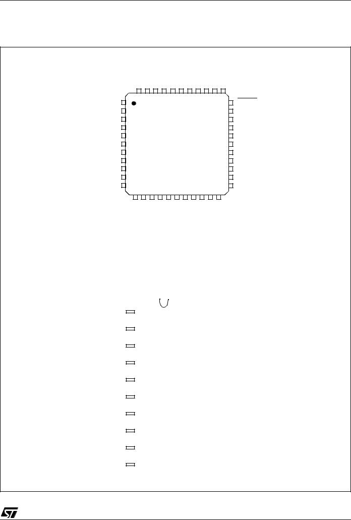
2 PIN DESCRIPTION
Figure 2. 44-pin TQFP and 42-Pin SDIP Package Pinouts
|
|
|
PD2 |
PD3 PD4 |
PD5 PD6 |
Reserved* |
V |
USBVCC |
USBDP USBDM |
V |
|
|
|
|
|
|
|
DDA |
|
|
SSA |
|
|
VPP |
44 43 42 41 40 39 38 37 36 35 34 |
|||||||
|
|
1 |
|
|
|
|
|
|
33 |
|
|
|
PD1 |
2 |
|
|
|
|
|
|
32 |
|
|
PD0 |
3 |
|
|
|
|
|
|
31 |
|
|
PC7 |
4 |
|
|
|
|
|
|
30 |
MOSI / PC6 |
5 |
|
|
|
|
|
|
29 |
||
IT12 / MISO / PC5 |
6 |
|
|
|
|
|
|
28 |
||
|
7 |
|
|
|
|
|
|
27 |
||
IT11 / |
SS |
/ PC4 |
|
|
|
|
|
|
||
IT10 / SCK / PC3 |
8 |
|
|
|
|
|
|
26 |
||
IT9 / PC2 |
9 |
|
|
|
|
|
|
25 |
||
|
OSCIN |
10 |
|
|
|
|
|
|
24 |
|
OSCOUT |
11 |
|
|
|
|
|
|
23 |
||
12 13 14 15 16 17 18 19 20 21 22
SS |
DD |
PC1 |
PC0 |
PB7 |
N.C. |
(HS) |
(HS) |
(HS) |
(HS) |
(HS) |
V |
V |
|||||||||
|
|
|
|
IT8 / PWM1 / |
|
/IT7 / PWM0 / PB6 |
IT6 / ARTIC2 / PB5 |
IT5 / ARTIC1 / PB4 |
ARTCLK / PB3 |
TDO / PB2 |
|
|
|
|
|
|
ICCDATA |
ICCCLK / |
|
|
|
RESET
PA0 / AIN0 / IT1 / USBOE
PA1 / AIN1 / IT2
PA2 / AIN2 / IT3
PA3 / AIN3 / IT4
PA4 / AIN4
PA5 / AIN5
PA6 / AIN6
PA7 / AIN7
PB0 (HS) / MCO
PB1 (HS) / RDI
* Pin 39 of the TQFP44 package must be left unconnected.
|
|
PD6 |
|
|
|
1 |
42 |
|
|
VDDA |
||
|
|
|
|
|
|
|
||||||
|
|
PD5 |
2 |
41 |
|
|
USBVCC |
|||||
|
|
|
|
|||||||||
|
|
PD4 |
|
|
3 |
40 |
|
|
|
USBDP |
||
|
|
|
|
|
|
|
||||||
|
|
PD3 |
4 |
39 |
|
|
|
USBDM |
||||
|
|
|
|
|
||||||||
|
|
PD2 |
|
|
5 |
38 |
|
|
|
VSSA |
|
|
|
|
|
|
|
|
|
||||||
|
|
VPP |
6 |
37 |
|
|
|
RESET |
||||
|
|
|
|
|
||||||||
|
|
PD1 |
|
|
7 |
36 |
|
|
|
PA0 / AIN0 / IT1 / USBOE |
||
|
|
|
|
|
|
|
||||||
|
|
PD0 |
8 |
35 |
|
|
|
PA1 / AIN1 / IT2 |
||||
|
|
|
|
|
||||||||
|
|
PC7 |
|
|
9 |
34 |
|
|
|
PA2 / AIN2 / IT3 |
||
|
|
|
|
|
|
|
||||||
MOSI / PC6 |
10 |
33 |
|
|
|
PA3 / AIN3 / IT4 |
||||||
|
|
|
||||||||||
IT12 / MISO / PC5 |
|
|
11 |
32 |
|
|
|
PA4 / AIN4 |
||||
|
|
|
|
|
||||||||
|
|
|
|
|
|
|
|
|
|
|
|
|
IT11 / SS / PC4 |
12 |
31 |
|
|
|
PA5 / AIN5 |
||||||
|
|
|
||||||||||
IT10 / SCK / PC3 |
|
|
13 |
30 |
|
|
|
PA6 / AIN6 |
||||
|
|
|
|
|
||||||||
IT9 / PC2 |
14 |
29 |
|
|
|
PA7 / AIN7 |
||||||
|
|
|
||||||||||
|
OSCIN |
|
|
15 |
28 |
|
|
|
PB0 (HS) / MCO |
|||
|
|
|
|
|
|
|||||||
OSCOUT |
16 |
27 |
|
|
|
PB1 (HS) / RDI |
||||||
|
|
|
||||||||||
|
|
VSS |
|
|
17 |
26 |
|
|
PB2 (HS) / TDO |
|||
|
|
|
|
|
|
|||||||
|
|
VDD |
18 |
25 |
|
|
PB3 (HS) / ARTCLK |
|||||
|
|
|
|
|||||||||
|
|
PC1 |
|
|
19 |
24 |
|
|
PB4 (HS) / ARTIC1 / IT5 |
|||
|
|
|
|
|
|
|||||||
|
|
PC0 |
20 |
23 |
|
|
PB5 (HS) / ARTIC2 / IT6 / ICCCLK |
|||||
|
|
|
|
|||||||||
IT8 / PWM1 / PB7 (HS) |
|
|
21 |
22 |
|
|
PB6 (HS) / PWM0 / IT7 / ICCDATA |
|||||
|
|
|
|
|||||||||
|
|
|
|
|
|
|
|
|
|
|
|
|
5/132

ST7262
PIN DESCRIPTION (Cont’d)
Figure 3. 34-Pin SO and 32-Pin SDIP Package Pinouts
|
|
|
|
|
|
|
|
|
IT10 / SCK / PC3 |
1 |
34 |
|
PC4 / SS / INT11 |
||||
IT9 / PC2 |
2 |
33 |
|
PC5 / MISO / IT12 |
||||
|
||||||||
OSCIN |
3 |
32 |
|
|
PC6 / MOSI |
|||
|
|
|||||||
OSCOUT |
4 |
31 |
|
PC7 |
||||
|
||||||||
VSS |
5 |
30 |
|
|
|
|
|
|
|
|
RESET |
|
|||||
|
|
|
|
|||||
|
|
|
|
|
||||
VDD |
6 |
29 |
|
|
VPP |
|||
|
|
|
||||||
PC1 |
7 |
28 |
|
|
VDDA |
|||
|
|
|||||||
|
|
|
||||||
IT8 / PWM1 / PB7 (HS) |
8 |
27 |
|
|
USBVCC |
|||
|
|
|||||||
ICCDATA / IT7 / PWM0 / PB6 (HS) |
9 |
26 |
|
|
USBDP |
|||
|
|
|||||||
ICCCLK / IT6 /ARTIC2 / PB5 (HS) |
10 |
25 |
|
|
USBDM |
|||
|
|
|||||||
IT5 / ARTIC1 / PB4 (HS) |
11 |
24 |
|
|
VSSA |
|||
|
|
|||||||
ARTCLK / PB3 (HS) |
12 |
23 |
|
|
||||
|
|
PA0 / AIN0 / IT1 / USBOE |
||||||
TDO / PB2 (HS) |
13 |
22 |
|
|
PA1 / AIN1 / IT2 |
|||
|
|
|||||||
RDI / PB1 (HS) |
14 |
21 |
|
|
PA2 / AIN2 / IT3 |
|||
|
|
|||||||
MCO / PB0 (HS) |
15 |
20 |
|
|
PA3 / AIN3 / IT4 |
|||
|
|
|||||||
AIN7 / PA7 |
16 |
19 |
|
|
PA4 / AIN4 |
|||
|
|
|||||||
AIN6 / PA6 |
17 |
18 |
|
PA5 / AIN5 |
||||
|
||||||||
|
|
|
|
|
|
|
|
|
|
|
|
|
|
|
|
|
|
|
IT10 / SCK / PC3 |
|
1 |
32 |
|
PC4 / SS / INT11 |
||||
|
|
||||||||
IT9 / PC2 |
|
2 |
31 |
|
PC5 / MISO / IT12 |
||||
|
|
||||||||
|
|
|
|
|
|
|
|||
OSCIN |
|
3 |
30 |
|
PC6 / MOSI |
||||
|
|
||||||||
OSCOUT |
|
|
|
|
|
||||
|
4 |
29 |
|
|
RESET |
|
|||
|
|
||||||||
VSS |
|
5 |
28 |
|
VPP |
||||
|
|
||||||||
|
|
||||||||
VDD |
|
6 |
27 |
|
VDDA |
||||
|
|
||||||||
IT8 / PWM1 / PB7 (HS) |
|
7 |
26 |
|
USBVCC |
||||
|
|
||||||||
ICCDATA / IT7 / PWM0 / PB6 (HS) |
|
8 |
25 |
|
|
USBDP |
|||
|
|
||||||||
ICCCLK / IT6 / ARTIC2 / PB5 (HS) |
|
9 |
24 |
|
USBDM |
||||
|
|
||||||||
IT5 / ARTIC1 / PB4 (HS) |
|
10 |
23 |
|
VSSA |
||||
|
|
||||||||
ARTCLK / PB3 (HS) |
|
|
|||||||
|
11 |
22 |
|
PA0 / AIN0 / IT1 / USBOE |
|||||
TDO / PB2 (HS) |
|
12 |
21 |
|
PA1 / AIN1 / IT2 |
||||
|
|
||||||||
RDI / PB1 (HS) |
|
13 |
20 |
|
PA2 / AIN2 / IT3 |
||||
|
|
||||||||
MCO / PB0 (HS) |
|
14 |
19 |
|
PA3 / AIN3 / IT4 |
||||
|
|
||||||||
AIN7 / PA7 |
|
15 |
18 |
|
PA4 / AIN4 |
||||
|
|
||||||||
AIN6 / PA6 |
|
16 |
17 |
|
PA5 / AIN5 |
||||
|
|
||||||||
|
|
|
|
|
|
|
|
|
|
6/132

ST7262
Figure 4. 20-pin SO20 Package Pinout
IT3 / AIN2 / PA2 |
1 |
20 |
|
PB0 (HS) / MCO |
||
|
||||||
|
PB1 (HS) |
|||||
IT2 / AIN1 / PA1 |
2 |
19 |
|
|||
|
||||||
|
PB2 (HS) |
|||||
USBOE/ IT1 / AIN0/ PA0 |
3 |
18 |
|
|||
|
||||||
|
|
|||||
|
VSS |
4 |
17 |
|
PB3 (HS) / ARTCLK |
|
|
|
|||||
|
|
PB4 (HS) / ARTIC1 / IT5 |
||||
USBDM |
5 |
16 |
|
|||
|
||||||
|
PB5 (HS) / ARTIC2 / IT6 / ICCCLK |
|||||
USBDP |
6 |
15 |
|
|||
|
||||||
USBVCC |
7 |
14 |
|
PB6 (HS) / PWM0 / IT7/ ICCDATA |
||
|
||||||
|
VDD |
8 |
13 |
|
PB7 (HS) / PWM1 / IT8 |
|
|
|
|||||
|
VPP |
9 |
12 |
|
OSCOUT |
|
|
|
|||||
|
|
|
|
|
|
|
|
RESET |
|
10 |
11 |
|
OSCIN |
|
|
|
||||
|
|
|
|
|
|
|
Figure 5. 20-pin DIP20 Package Pinout
IT5 / ARTIC1 / PB4 (HS) |
|
|
|
|
PB5 (HS) / ARTIC2 / IT6 / ICCCLK |
|
1 |
20 |
|
|
|||
|
|
|||||
ARTCLK / PB3 (HS) |
2 |
19 |
|
|
PB6 (HS) / PWM0 / IT7/ICCDATA |
|
|
|
|||||
|
|
|||||
PB2 (HS) |
3 |
18 |
|
|
PB7 (HS) / PWM1 / IT8 |
|
|
|
|||||
PB1 (HS) |
|
|
||||
4 |
17 |
|
|
OSCOUT |
||
|
|
|||||
|
|
|||||
MCO / PB0 (HS) |
5 |
16 |
|
|
OSCIN |
|
|
|
|||||
IT3 / AIN2 / PA2 |
|
|
|
|
|
|
6 |
15 |
|
|
RESET |
|
|
|
|
|
||||
IT2 / AIN1/ PA1 |
7 |
14 |
|
|
VPP |
|
|
|
|||||
USBOE / IT1 / AIN0 / PA0 |
8 |
13 |
|
|
VDD |
|
|
|
|||||
VSS |
9 |
12 |
|
|
USBVCC |
|
|
|
|||||
USBDM |
10 |
11 |
|
|
USBDP |
|
|
|
|||||
|
|
|
|
|
|
|
|
|
|
|
|
|
|
7/132

ST7262
PIN DESCRIPTION (Cont’d)
Legend / Abbreviations:
Type: |
I = Input, O = Output, S = Supply |
Input level: |
A = Dedicated analog input |
Input level: |
C = CMOS 0.3VDD/0.7VDD, |
|
CT= CMOS 0.3VDD/0.7VDD with input trigger |
Output level: |
HS = High Sink (on N-buffer only) |
Port configuration capabilities:
–Input:float = floating, wpu = weak pull-up, int = interrupt (\ =falling edge, / =rising edge), ana = analog
–Output: OD = open drain, T = true open drain (N buffer 8mA@0.4 V), PP = push-pull
Table 1. Device Pin Description
|
|
Pin n° |
|
|
|
|
|
|
|
Level |
|
Port / Control |
|
Main |
|
|||||
|
|
|
|
|
|
|
|
|
|
|
|
|
|
|
|
|
|
|
|
|
TQFP44 |
DIP42 |
SO34 |
DIP32 |
SO20 |
DIP20 |
|
|
|
Type |
Input |
Output |
float |
wpu |
int |
ana |
OD |
PP |
Function |
|
|
|
|
|
|
|
|
Pin Name |
|
|
|
|
|
Input |
|
Output |
Alternate Function |
|||||
|
|
|
|
|
|
|
|
|
|
|
|
|
|
|
|
|
|
|
(after |
|
|
|
|
|
|
|
|
|
|
|
|
|
|
|
|
|
|
|
|
reset) |
|
|
|
|
|
|
|
|
|
|
|
|
|
|
|
|
|
|
|
|
|
|
|
|
|
|
|
|
|
|
|
|
|
|
|
|
|
|
|
|
|
FLASH programming voltage |
|
1 |
6 |
29 |
28 |
9 |
14 |
VPP |
S |
|
|
|
x |
|
|
|
|
(12V), must be tied low in user |
||||
|
|
|
|
|
|
|
|
|
|
|
|
|
|
|
|
|
|
|
mode. |
|
|
|
|
|
|
|
|
|
|
|
|
|
|
|
|
|
|
|
|
||
2 |
7 |
- |
- |
- |
- |
PD1 |
I/O |
CT |
|
|
x |
|
|
|
x |
Port D1 |
|
|||
3 |
8 |
- |
- |
- |
- |
PD0 |
I/O |
CT |
|
|
x |
|
|
|
x |
Port D0 |
|
|||
4 |
9 |
31 |
- |
- |
- |
PC7 |
I/O |
CT |
|
|
x |
|
|
|
x |
Port C7 |
|
|||
5 |
10 |
32 |
30 |
- |
- |
PC6/MOSI |
I/O |
CT |
|
|
x |
|
|
|
x |
Port C6 |
SPI Master Out / |
|||
|
|
|
|
|
Slave In 1) |
|||||||||||||||
|
|
|
|
|
|
|
|
|
|
|
|
|
|
|
|
|
|
|
|
SPI Master In / |
6 |
11 |
33 |
31 |
- |
- |
PC5/MISO/IT12 |
I/O |
CT |
|
|
x |
x |
|
|
x |
Port C5 |
Slave Out 1) / |
|||
|
|
|
|
|
|
|
|
|
|
|
|
|
|
|
|
|
|
|
|
Interrupt 12 input |
|
|
|
|
|
|
|
|
|
|
|
|
|
|
|
|
|
|
|
|
|
|
|
|
|
|
|
|
|
|
|
|
|
|
|
|
|
|
|
|
|
SPI Slave Select |
7 |
12 |
34 |
32 |
- |
- |
PC4/SS/IT11 |
I/O |
CT |
|
|
x |
x |
|
|
x |
Port C4 |
(active low) 1)/ |
|||
|
|
|
|
|
|
|
|
|
|
|
|
|
|
|
|
|
|
|
|
Interrupt 11 input |
|
|
|
|
|
|
|
|
|
|
|
|
|
|
|
|
|
|
|
|
|
8 |
13 |
1 |
1 |
- |
- |
PC3/SCK/IT10 |
I/O |
CT |
|
|
x |
x |
|
|
x |
Port C3 |
SPI Serial Clock 1)/ |
|||
|
|
|
|
Interrupt 10 input |
||||||||||||||||
|
|
|
|
|
|
|
|
|
|
|
|
|
|
|
|
|
|
|||
9 |
14 |
2 |
2 |
- |
- |
PC2/IT9 |
I/O |
CT |
|
|
x |
x |
|
|
x |
Port C2 |
Interrupt 9 input |
|||
10 |
15 |
3 |
3 |
11 |
16 |
OSCIN |
|
|
|
|
|
|
|
|
|
|
These pins |
are used connect an |
||
|
|
|
|
|
|
|
|
|
|
|
|
|
|
|
|
|
|
|
external clock source to the on- |
|
11 |
16 |
4 |
4 |
12 |
17 |
OSCOUT |
|
|
|
|
|
|
|
|
|
|
||||
|
|
|
|
|
|
|
|
|
|
chip main oscillator. |
||||||||||
|
|
|
|
|
|
|
|
|
|
|
|
|
|
|
|
|
||||
12 |
17 |
5 |
5 |
4 |
9 |
VSS |
S |
|
|
|
|
|
|
|
|
Digital Ground Voltage |
||||
13 |
18 |
6 |
6 |
8 |
13 |
VDD |
S |
|
|
|
|
|
|
|
|
Digital Main Power Supply Volt- |
||||
|
|
|
|
|
|
|
|
age |
|
|||||||||||
14 |
19 |
7 |
- |
- |
- |
PC1 |
I/O |
CT |
|
x |
|
|
|
T |
|
Port C1 |
|
|||
15 |
20 |
- |
- |
- |
- |
PC0 |
I/O |
CT |
|
x |
|
|
|
T |
|
Port C0 |
|
|||
|
|
|
|
|
|
PB7/PWM1/IT8/ |
|
|
|
|
|
|
|
|
|
|
|
ART PWM output 1/ |
||
16 |
21 |
8 |
7 |
13 |
18 |
RX_SEZ/DA- |
I/O |
CT |
HS |
x |
|
\ |
|
|
x |
Port B7 |
||||
|
|
|
Interrupt 8 input |
|||||||||||||||||
|
|
|
|
|
|
TAOUT/DA9 |
|
|
|
|
|
|
|
|
|
|
|
|
||
17 |
- |
- |
|
|
|
N.C. |
|
|
|
|
|
|
|
|
|
|
Not Connected |
|||
|
|
|
|
|
|
|
|
|
|
|
|
|
|
|
|
|
|
|
|
|
8/132

|
|
|
|
|
|
|
|
|
|
|
|
|
|
|
|
|
|
|
|
ST7262 |
|
|
|
|
|
|
|
|
|
|
|
|
|
|
|
|
|
|
|
|
|
|
|
Pin n° |
|
|
|
|
|
|
|
Level |
|
Port / Control |
|
Main |
|
|||||
|
|
|
|
|
|
|
|
|
|
|
|
|
|
|
|
|
|
|
|
|
TQFP44 |
DIP42 |
SO34 |
DIP32 |
SO20 |
DIP20 |
|
|
|
Type |
Input |
Output |
float |
wpu |
int |
ana |
OD |
PP |
Function |
|
|
|
|
|
|
|
|
|
Pin Name |
|
|
|
|
|
Input |
|
Output |
Alternate Function |
||||
|
|
|
|
|
|
|
|
|
|
|
|
|
|
|
|
|
|
|
(after |
|
|
|
|
|
|
|
|
|
|
|
|
|
|
|
|
|
|
|
|
reset) |
|
|
|
|
|
|
|
|
|
|
|
|
|
|
|
|
|
|
|
|
|
|
|
|
|
|
|
|
|
|
|
|
|
|
|
|
|
|
|
|
|
|
ART PWM output 0/ |
18 |
22 |
9 |
8 |
14 |
19 |
PB6/PWM0/IT7/ |
I/O |
CT |
HS |
x |
|
\ |
|
|
x |
Port B6 |
Interrupt 7 input/In- |
|||
ICCDATA |
|
|
|
Circuit Communica- |
||||||||||||||||
|
|
|
|
|
|
|
|
|
|
|
|
|
|
|
|
|
|
|
|
tion Data |
|
|
|
|
|
|
|
|
|
|
|
|
|
|
|
|
|
|
|
|
|
|
|
|
|
|
|
|
|
|
|
|
|
|
|
|
|
|
|
|
|
ART Input Capture 2/ |
19 |
23 |
10 |
9 |
15 |
20 |
PB5/ARTIC2/IT6/ |
I/O |
CT |
HS |
x |
|
/ |
|
|
x |
Port B5 |
Interrupt 6 input/ |
|||
ICCCLK |
|
|
|
In-Circuit Communi- |
||||||||||||||||
|
|
|
|
|
|
|
|
|
|
|
|
|
|
|
|
|
|
|
|
cation Clock |
|
|
|
|
|
|
|
|
|
|
|
|
|
|
|
|
|
|
|
|
|
20 |
24 |
11 |
10 |
16 |
1 |
PB4/ARTIC1/IT5 |
I/O |
CT |
HS |
x |
|
/ |
|
|
x |
Port B4 |
ART Input Capture |
|||
|
|
|
1/Interrupt 5 input |
|||||||||||||||||
21 |
25 |
12 |
11 |
17 |
2 |
PB3/ARTCLK |
I/O |
CT |
HS |
x |
|
|
|
|
x |
Port B3 |
ART Clock input |
|||
22 |
26 |
13 |
12 |
18 |
3 |
PB2/TDO |
I/O |
CT |
HS |
x |
|
|
|
|
x |
Port B2 |
SCI Transmit Data |
|||
|
|
|
|
Output 1) |
||||||||||||||||
23 |
27 |
14 |
13 |
19 |
4 |
|
PB1/RDI |
I/O |
CT |
HS |
x |
|
|
|
|
x |
Port B1 |
SCI Receive Data |
||
|
|
|
|
|
Input 1) |
|||||||||||||||
24 |
28 |
15 |
14 |
20 |
5 |
|
PB0/MCO |
I/O |
CT |
HS |
x |
|
|
|
|
x |
Port B0 |
CPU clock output |
||
25 |
29 |
16 |
15 |
- |
- |
PA7/AIN7 |
I/O |
CT |
|
x |
|
|
x |
|
x |
Port A7 |
ADC Analog Input 7 |
|||
26 |
30 |
17 |
16 |
- |
- |
|
PA6/AIN6 |
I/O |
CT |
|
x |
|
|
x |
|
x |
Port A6 |
ADC Analog Input 6 |
||
27 |
31 |
18 |
17 |
- |
- |
|
PA5/AIN5 |
I/O |
CT |
|
x |
|
|
x |
|
x |
Port A5 |
ADC Analog Input 5 |
||
28 |
32 |
19 |
18 |
- |
- |
|
PA4/AIN4 |
I/O |
CT |
|
x |
|
|
x |
|
x |
Port A4 |
ADC Analog Input 4 |
||
29 |
33 |
20 |
19 |
- |
- |
|
PA3/AIN3/IT4 |
I/O |
CT |
|
x |
|
\ |
x |
|
x |
Port A3 |
ADC Analog Input 3/ |
||
|
|
|
|
Interrupt 4 input |
||||||||||||||||
|
|
|
|
|
|
|
|
|
|
|
|
|
|
|
|
|
|
|
|
|
30 |
34 |
21 |
20 |
1 |
6 |
|
PA2/AIN2/IT3 |
I/O |
CT |
|
x |
|
\ |
x |
|
x |
Port A2 |
ADC Analog Input 2/ |
||
|
|
|
|
Interrupt 3 input |
||||||||||||||||
|
|
|
|
|
|
|
|
|
|
|
|
|
|
|
|
|
|
|
|
|
31 |
35 |
22 |
21 |
2 |
7 |
|
PA1/AIN1/IT2 |
I/O |
CT |
|
x |
|
\ |
x |
|
x |
Port A1 |
ADC Analog Input 1/ |
||
|
|
|
|
Interrupt 2 input |
||||||||||||||||
|
|
|
|
|
|
|
|
|
|
|
|
|
|
|
|
|
|
|
|
|
|
|
|
|
|
|
PA0/AIN0/IT1/ |
|
|
|
|
|
|
|
|
|
|
|
ADC Analog Input 0/ |
||
32 |
36 |
23 |
22 |
3 |
8 |
I/O |
CT |
|
x |
|
\ |
x |
|
x |
Port A0 |
Interrupt 1 input/ |
||||
USBOE |
|
|
|
|||||||||||||||||
|
|
|
|
|
|
|
|
|
|
|
|
|
|
|
|
|
|
|
|
USB Output Enable |
|
|
|
|
|
|
|
|
|
|
|
|
|
|
|
|
|
|
|
Top priority |
non maskable inter- |
33 |
37 |
30 |
29 |
10 |
15 |
|
RESET |
I/O |
C |
|
|
|
|
|
|
|
||||
|
|
|
|
|
|
|
|
rupt (active low) |
||||||||||||
|
|
|
|
|
|
|
|
|
|
|
|
|
|
|
|
|
|
|
||
|
|
|
|
|
|
|
|
|
|
|
|
|
|
|
|
|
|
|
|
|
34 |
38 |
24 |
23 |
- |
- |
|
VSSA |
S |
|
|
|
|
|
|
|
|
Analog Ground Voltage, must |
|||
|
|
|
|
|
|
|
|
|
be connected externally to VSS. |
|||||||||||
|
|
|
|
|
|
|
|
|
|
|
|
|
|
|
|
|
|
|
||
35 |
39 |
25 |
24 |
5 |
10 |
|
USBDM |
I/O |
|
|
|
|
|
|
|
|
USB bidirectional data (data -) |
|||
|
|
|
|
|
|
|
|
|
|
|
|
|
|
|
|
|
|
|||
36 |
40 |
26 |
25 |
6 |
11 |
|
USBDP |
I/O |
|
|
|
|
|
|
|
|
USB bidirectional data (data +) |
|||
|
|
|
|
|
|
|
|
|
|
|
|
|
|
|
|
|
|
|||
37 |
41 |
27 |
26 |
7 |
12 |
|
USBVCC |
S |
|
|
|
|
|
|
|
|
USB power supply 3.3V output |
|||
|
|
|
|
|
|
|
|
|
|
|
|
|
|
|
|
|
|
|
|
|
|
|
|
|
|
|
|
|
|
|
|
|
|
|
|
|
|
|
|
Analog Power Supply Voltage, |
|
38 |
42 |
28 |
27 |
- |
- |
|
VDDA |
S |
|
|
|
|
|
|
|
|
must be connected externally to |
|||
|
|
|
|
|
|
|
|
|
|
|
|
|
|
|
|
|
|
|
VDD. |
|
39 |
- |
- |
- |
- |
- |
|
Reserved |
|
|
|
|
|
|
|
|
|
|
Must be left unconnected. |
||
|
|
|
|
|
|
|
|
|
|
|
|
|
|
|
|
|
|
|
||
40 |
1 |
- |
- |
- |
- |
|
PD6 |
I/O |
CT |
|
|
x |
|
|
|
x |
Port D6 |
|
||
41 |
2 |
- |
- |
- |
- |
|
PD5 |
I/O |
CT |
|
|
x |
|
|
|
x |
Port D5 |
|
||
42 |
3 |
- |
- |
- |
- |
|
PD4 |
I/O |
CT |
|
|
x |
|
|
|
x |
Port D4 |
|
||
9/132
ST7262
|
|
Pin n° |
|
|
|
|
|
Level |
|
Port / Control |
|
Main |
|
|||||
|
|
|
|
|
|
|
|
|
|
|
|
|
|
|
|
|
|
|
TQFP44 |
DIP42 |
SO34 |
DIP32 |
SO20 |
DIP20 |
|
Type |
Input |
Output |
float |
wpu |
int |
ana |
OD |
PP |
Function |
|
|
|
|
|
|
|
|
Pin Name |
|
|
|
|
|
Input |
|
Output |
Alternate Function |
|||
|
|
|
|
|
|
|
|
|
|
|
|
|
|
|
|
|
(after |
|
|
|
|
|
|
|
|
|
|
|
|
|
|
|
|
|
|
reset) |
|
|
|
|
|
|
|
|
|
|
|
|
|
|
|
|
|
|
|
|
43 |
4 |
- |
- |
- |
- |
PD3 |
I/O |
CT |
|
|
x |
|
|
|
x |
Port D3 |
|
|
44 |
5 |
- |
- |
- |
- |
PD2 |
I/O |
CT |
|
|
x |
|
|
|
x |
Port D2 |
|
|
Note 1: Peripheral not present on all devices. Refer to “Device Summary” on page 1.
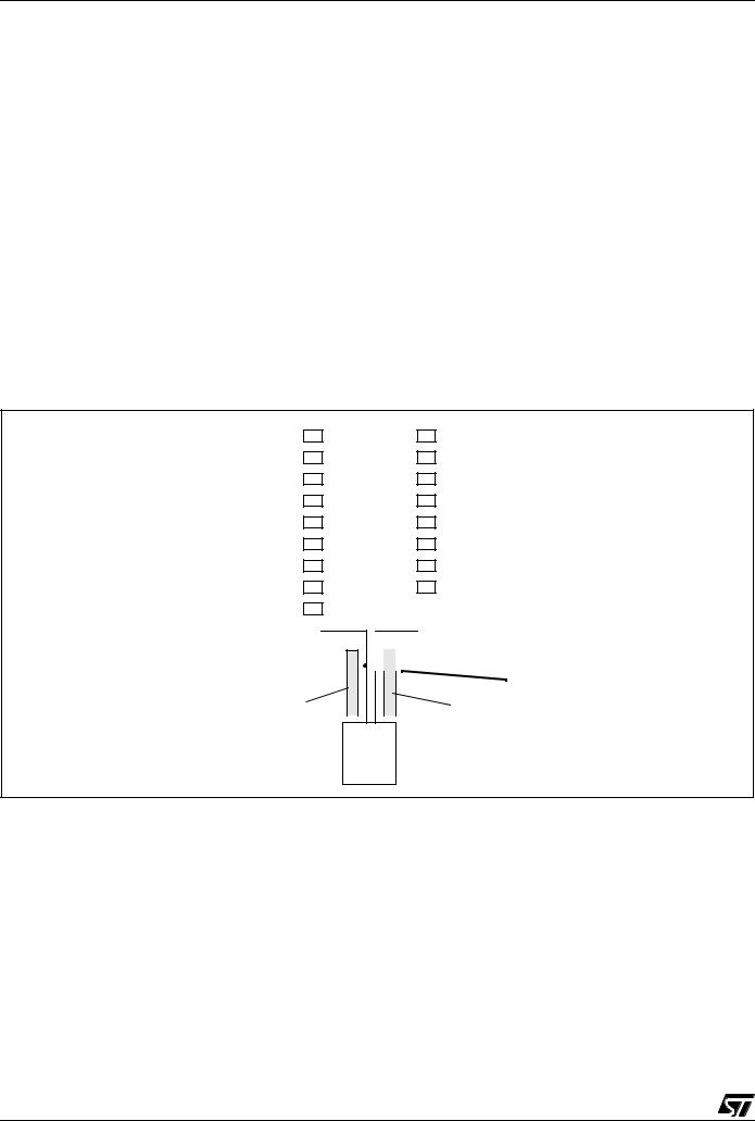
2.1 PCB LAYOUT RECOMMENDATION
In the case of DIP20 devices the user should layout the PCB so that the DIP20 ST7262 device and the USB connector are centered on the same axis ensuring that the D- and D+ lines are of equal length. Refer to Figure 6
Figure 6. Recommended PCB Layout for USB Interface with DIP20 package
|
|
1 |
|
|
|
20 |
|
|
|
|
||
|
|
|
|
|
|
|
|
|
||||
|
|
|
|
|
|
|
|
|
||||
|
|
2 |
|
|
|
19 |
|
|
|
|
||
|
|
|
|
|
|
|
|
|
||||
|
|
|
|
|
|
|
|
|
||||
|
|
3 |
|
|
|
18 |
|
|
|
|
||
|
|
|
|
|
|
|
|
|
||||
|
|
|
|
|
|
|
|
|
||||
|
|
4 |
|
|
|
17 |
|
|
|
|
||
|
|
|
|
|
|
|
|
|
||||
|
|
|
|
|
|
|
|
|
||||
|
|
5 |
ST7262 |
16 |
|
|
|
|
||||
|
|
|
|
|
|
|||||||
|
|
|
|
|
|
|||||||
|
|
6 |
15 |
|
|
|
|
|||||
|
|
|
|
|
|
|||||||
|
|
|
|
|
|
|
|
|
||||
|
|
7 |
|
|
|
14 |
|
|
|
|
||
|
|
|
|
|
|
|
|
|
||||
|
|
|
|
|
|
|
|
|
||||
|
|
8 |
|
|
|
13 |
|
|
|
USBVCC |
||
|
|
|
|
|
|
|
|
|||||
|
|
|
|
|
|
|
|
|||||
USBDM |
|
9 |
|
|
|
12 |
|
|
|
|||
|
|
|
|
|
|
|||||||
|
10 |
|
|
|
11 |
|
|
|
USBDP |
|||
|
|
|
|
|
|
|||||||
|
|
|
|
|
|
|||||||
|
|
|
|
|
|
|
|
|
|
|
|
|
|
|
|
|
|
|
|
|
|
|
|
|
|
|
|
|
|
|
|
|
|
|
|
|
|
|
|
|
|
|
|
|
|
|
|
|
|
|
|
|
|
|
|
|
|
|
|
|
|
|
|
|
1.5KOhm pull-up resistor
Ground |
|
|
|
Ground |
|
|
USB Connector
10/132
ST7262
3 REGISTER & MEMORY MAP
As shown in the Figure 7, the MCU is capable of addressing 64K bytes of memories and I/O registers.
The available memory locations consist of 64 bytes of register locations, 768 bytes of RAM and up to 16 Kbytes of user program memory. The RAM space includes up to 128 bytes for the stack from 0100h to 017Fh.
The highest address bytes contain the user reset and interrupt vectors.
Figure 7. Memory Map
IMPORTANT: Memory locations marked as “Reserved” must never be accessed. Accessing a reseved area can have unpredictable effects on the device.
|
|
|
|
|
|
|
|
|
|
|
|
0040h |
|
|
|
|
|
|
|
|
|
|
|
|
|
|
Short Addressing |
|
|
0000h |
|
|
|
|
|
|
|
|
|
|
|
|
RAM (zero page) |
|
HW Registers |
|
|
|
|
|
|
|
|
|
192 Bytes |
|
|||
|
|
|
|
|
|
|
|
|
00FFh |
|
||||
|
|
(see Table 2) |
|
|
|
|
|
|
|
|
|
|
||
003Fh |
|
|
|
|
|
|
|
|
|
|
16-bit Addressing |
|
||
|
|
|
|
|
|
|
|
|
|
|
|
|
||
|
|
|
|
|
|
|
|
|
|
|
|
RAM |
|
|
0040h |
|
|
|
|
|
|
|
|
|
|
|
|
|
|
|
|
|
|
|
|
|
|
|
|
|
|
or Stack |
|
|
|
|
384 Bytes RAM |
|
|
|
|
|
|
|
|
|
|
||
|
|
|
|
|
|
|
|
|
|
017Fh |
(128 Bytes) |
|
||
|
|
|
|
|
|
|
|
|
|
|
|
|
||
|
|
|
|
|
|
|
|
|
|
|
|
|
16-bit Addressing |
|
|
|
|
|
|
|
|
|
|
|
|
|
|
|
|
|
|
|
|
|
|
|
|
|
|
|
|
|
RAM |
|
|
768 Bytes RAM |
|
|
|
|
|
|
|
|
01BFh |
64 Bytes |
|
||
033Fh |
|
|
|
|
|
|
|
|
|
|
|
|
|
|
|
|
|
|
|
||||||||||
|
|
|
|
|
|
|
|
|
|
|
|
|
|
|
|
|
|
|
|
|
|
|
|
|
|
|
|
|
|
|
|
|
|
|
|
|
|
|
|
|
|
|
|
|
0340h |
|
|
|
|
|
|
|
|
|
|
|
|
|
|
|
Reserved |
|
|
|
|
|
|
|
|
0040h |
Short Addressing |
|
||
BFFFh |
|
|
|
|
|
|
|
|
|
|
||||
|
|
|
|
|
|
|
|
|
|
|||||
|
|
|
|
|
|
|
|
|
|
|
|
RAM (zero page) |
|
|
|
|
|
|
|
|
|
|
|
|
|
|
|
||
C000h |
Program Memory |
|
|
|
|
|
|
|
|
00FFh |
192 Bytes |
|
||
|
|
|
|
|
|
|
|
|
||||||
|
|
|
|
|
|
|
|
|
|
|
||||
|
|
|
|
|
|
|
|
|
16-bit Addressing |
|
||||
|
|
|
|
|
|
|
|
|
|
|
|
|
|
|
|
|
16 KBytes |
|
|
|
|
|
|
|
|
|
RAM |
|
|
E000h |
|
|
|
|
|
|
|
|
|
|
|
|
or Stack |
|
|
|
|
|
|
|
|
|
|
|
|
|
|
||
|
|
|
|
|
|
|
|
|
|
|
017Fh |
(128 Bytes) |
|
|
|
|
|
|
|
|
|
|
|
|
|
|
|
|
|
|
8 KBytes |
|
|
|
|
|
|
|
|
|
|
16-bit Addressing |
|
|
|
|
|
|
|
|
|
|
|
|
|
RAM |
|
||
|
|
|
|
|
|
|
|
|
|
|
|
|
|
|
FFDFh |
|
|
|
|
|
|
|
|
|
|
|
033Fh |
448 Bytes |
|
FFE0h |
Interrupt & Reset Vectors |
|
|
|
|
|
|
|
|
|
|
|||
|
|
|
|
|
|
|
|
|
|
|
||||
|
|
|
|
|
|
|
|
|
|
|
|
|||
|
|
(see Table 6) |
|
|
|
|
|
|
|
|
|
|
|
|
FFFFh |
|
|
|
|
|
|
|
|
|
|
|
|
|
|
|
|
|
|
|
|
|
|
|
|
|
|
|
|
|
|
|
|
|
|
|
|
|
|
|
|
|
|
|
|
11/132

ST7262
Table 2. Hardware Register Map
Address |
Block |
Register |
Register Name |
Reset |
Remarks |
|
Label |
Status |
|||||
|
|
|
|
|||
|
|
|
|
|
|
|
0000h |
Port A |
PADR |
Port A Data Register |
00h1) |
R/W2) |
|
0001h |
PADDR |
Port A Data Direction Register |
00h |
R/W2) |
||
|
||||||
|
|
|
|
|
|
|
0002h |
Port B |
PBDR |
Port B Data Register |
00h1) |
R/W2) |
|
0003h |
PBDDR |
Port B Data Direction Register |
00h |
R/W2) |
||
|
||||||
|
|
|
|
|
|
|
0004h |
Port C |
PCDR |
Port C Data Register |
00h1) |
R/W2) |
|
0005h |
PCDDR |
Port C Data Direction Register |
00h |
R/W2) |
||
|
||||||
|
|
|
|
|
|
|
0006h |
Port D |
PDDR |
Port D Data Register |
00h1) |
R/W2) |
|
0007h |
PDDDR |
Port D Data Direction Register |
00h |
R/W2) |
||
|
||||||
|
|
|
|
|
|
|
0008h |
|
ITRFRE1 |
Interrupt Register 1 |
00h |
R/W |
|
|
|
|
|
|
|
|
0009h |
|
MISC |
Miscellaneous Register |
00h |
R/W |
|
|
|
|
|
|
|
|
000Ah |
|
ADCDRMSB |
ADC Data Register (bit 9:2) |
00h |
Read Only |
|
000Bh |
ADC |
ADCDRLSB |
ADC Data Register (bit 1:0) |
00h |
Read Only |
|
000Ch |
|
ADCCSR |
ADC Control Status Register |
00h |
R/W |
|
|
|
|
|
|
|
|
000Dh |
WDG |
WDGCR |
Watchdog Control Register |
7Fh |
R/W |
|
|
|
|
|
|
|
|
000Eh |
|
|
Reserved Area (3 Bytes) |
|
|
|
0010h |
|
|
|
|
||
|
|
|
|
|
||
|
|
|
|
|
|
|
0011h |
|
SPIDR |
SPI Data I/O Register |
xxh |
R/W |
|
0012h |
SPI |
SPICR |
SPI Control Register |
0xh |
R/W |
|
0013h |
|
SPICSR |
SPI Control Status Register |
00h |
Read Only |
|
|
|
|
|
|
|
|
0014h |
|
PWMDCR1 |
PWM AR Timer Duty Cycle Register 1 |
00h |
R/W |
|
0015h |
|
PWMDCR0 |
PWM AR Timer Duty Cycle Register 0 |
00h |
R/W |
|
0016h |
|
PWMCR |
PWM AR Timer Control Register |
00h |
R/W |
|
0017h |
|
ARTCSR |
Auto-Reload Timer Control/Status Register |
00h |
R/W |
|
0018h |
PWM ART |
ARTCAR |
Auto-Reload Timer Counter Access Register |
00h |
R/W |
|
0019h |
|
ARTARR |
Auto-Reload Timer Auto-Reload Register |
00h |
R/W |
|
001Ah |
|
ARTICCSR |
ART Input Capture Control/Status Register |
00h |
R/W |
|
001Bh |
|
ARTICR1 |
ART Input Capture Register 1 |
00h |
Read Only |
|
001Ch |
|
ARTICR2 |
ART Input Capture Register 2 |
00h |
Read Only |
|
|
|
|
|
|
|
|
001Dh |
|
SCIERPR |
SCI Extended Receive Prescaler register |
00h |
R/W |
|
001Eh |
|
SCIETPR |
SCI Extended Transmit Prescaler Register |
00h |
R/W |
|
001Fh |
|
|
Reserved Area |
-- |
|
|
0020h |
SCI |
SCISR |
SCI Status register |
C0h |
Read Only |
|
0021h |
SCIDR |
SCI Data register |
xxh |
R/W |
||
|
||||||
0022h |
|
SCIBRR |
SCI Baud Rate Register |
00h |
R/W |
|
0023h |
|
SCICR1 |
SCI Control Register 1 |
x000 0000b |
R/W |
|
0024h |
|
SCICR2 |
SCI Control Register 2 |
00h |
R/W |
|
|
|
|
|
|
|
12/132

|
|
|
|
|
ST7262 |
|
|
|
|
|
|
|
|
Address |
Block |
Register |
Register Name |
Reset |
Remarks |
|
Label |
Status |
|||||
|
|
|
|
|||
|
|
|
|
|
|
|
0025h |
|
USBPIDR |
USB PID Register |
x0h |
Read Only |
|
0026h |
|
USBDMAR |
USB DMA Address register |
xxh |
R/W |
|
0027h |
|
USBIDR |
USB Interrupt/DMA Register |
x0h |
R/W |
|
0028h |
|
USBISTR |
USB Interrupt Status Register |
00h |
R/W |
|
0029h |
|
USBIMR |
USB Interrupt Mask Register |
00h |
R/W |
|
002Ah |
|
USBCTLR |
USB Control Register |
06h |
R/W |
|
002Bh |
USB |
USBDADDR |
USB Device Address Register |
00h |
R/W |
|
002Ch |
|
USBEP0RA |
USB Endpoint 0 Register A |
0000 xxxxb |
R/W |
|
002Dh |
|
USBEP0RB |
USB Endpoint 0 Register B |
80h |
R/W |
|
002Eh |
|
USBEP1RA |
USB Endpoint 1 Register A |
0000 xxxxb |
R/W |
|
002Fh |
|
USBEP1RB |
USB Endpoint 1 Register B |
0000 xxxxb |
R/W |
|
0030h |
|
USBEP2RA |
USB Endpoint 2 Register A |
0000 xxxxb |
R/W |
|
0031h |
|
USBEP2RB |
USB Endpoint 2 Register B |
0000 xxxxb |
R/W |
|
|
|
|
|
|
|
|
0032h |
|
|
|
|
|
|
to |
|
|
Reserved Area (4 Bytes) |
|
|
|
0035h |
|
|
|
|
|
|
|
|
|
|
|
|
|
0032h |
|
ITSPR0 |
Interrupt Software Priority Register 0 |
FFh |
R/W |
|
0033h |
ITC |
ITSPR1 |
Interrupt Software Priority Register1 |
FFh |
R/W |
|
0034h |
ITSPR2 |
Interrupt Software Priority Register 2 |
FFh |
R/W |
||
|
||||||
0035h |
|
ITSPR3 |
Interrupt Software Priority Register 3 |
FFh |
R/W |
|
|
|
|
|
|
|
|
0036h |
TBU |
TBUCV |
TBU Counter Value Register |
00h |
R/W |
|
0037h |
TBUCSR |
TBU Control/Status Register |
00h |
R/W |
||
|
||||||
|
|
|
|
|
|
|
0038h |
FLASH |
FCSR |
Flash Control/Status Register |
00h |
R/W |
|
|
|
|
|
|
|
|
0039h |
|
ITRFRE2 |
Interrupt Register 2 |
00h |
R/W |
|
|
|
|
|
|
|
|
003Ah |
|
|
|
|
|
|
to |
|
|
Reserved Area (6 Bytes) |
|
|
|
003Fh |
|
|
|
|
|
|
|
|
|
|
|
|
Legend: x=undefined, R/W=read/write
Notes:
1.The contents of the I/O port DR registers are readable only in output configuration. In input configuration, the values of the I/O pins are returned instead of the DR register contents.
2.The bits associated with unavailable pins must always be kept at their reset value.
13/132

ST7262
4 FLASH PROGRAM MEMORY
4.1 Introduction
The ST7 dual voltage High Density Flash (HDFlash) is a non-volatile memory that can be electrically erased as a single block or by individual sectors and programmed on a Byte-by-Byte basis using an external VPP supply.
The HDFlash devices can be programmed and erased off-board (plugged in a programming tool) or on-board using ICP (In-Circuit Programming) or IAP (In-Application Programming).
The array matrix organisation allows each sector to be erased and reprogrammed without affecting other sectors.
4.2 Main Features
■Three Flash programming modes:
–Insertion in a programming tool. In this mode, all sectors including option bytes can be programmed or erased.
–ICP (In-Circuit Programming). In this mode, all sectors including option bytes can be programmed or erased without removing the device from the application board.
–IAP (In-Application Programming) In this mode, all sectors except Sector 0, can be programmed or erased without removing the device from the application board and while the application is running.
■ICT (In-Circuit Testing) for downloading and executing user application test patterns in RAM
■Read-out protection against piracy
■Register Access Security System (RASS) to prevent accidental programming or erasing
4.3 Structure
The Flash memory is organised in sectors and can be used for both code and data storage.
Figure 8. Memory Map and Sector Address
Depending on the overall Flash memory size in the microcontroller device, there are up to three user sectors (see Table 3). Each of these sectors can be erased independently to avoid unnecessary erasing of the whole Flash memory when only a partial erasing is required.
The first two sectors have a fixed size of 4 Kbytes (see Figure 8). They are mapped in the upper part of the ST7 addressing space so the reset and interrupt vectors are located in Sector 0 (F000hFFFFh).
Table 3. Sectors available in Flash devices
Flash Size (bytes) |
Available Sectors |
|
|
4K |
Sector 0 |
|
|
8K |
Sectors 0,1 |
|
|
> 8K |
Sectors 0,1, 2 |
|
|
4.3.1 Read-out Protection
Read-out protection, when selected, makes it impossible to extract the memory content from the microcontroller, thus preventing piracy. Even ST cannot access the user code.
In flash devices, this protection is removed by reprogramming the option. In this case, the entire program memory is first automatically erased and the device can be reprogrammed.
Read-out protection selection depends on the device type:
–In Flash devices it is enabled and removed through the FMP_R bit in the option byte.
–In ROM devices it is enabled by mask option specified in the Option List.
|
|
4K |
|
|
8K |
|
|
|
10K |
|
|
16K |
|
|
|
24K |
|
|
32K |
|
|
|
48K |
|
|
60K |
|
|
|
FLASH |
||||||||||
|
|
|
|
|
|
|
|
|
|
|
|
|
|
|
|
|
|
|
|
|
|
|
|
|
|
|
|
|
|
|
|
|
|
|
|
|
|
|
|
MEMORY SIZE |
1000h |
|
|
|
|
|
|
|
|
|
|
|
|
|
|
|
|
|
|
|
|
|
|
|
|
|
|
|
|
|
|
|
|
|
|||||||
3FFFh |
|
|
|
|
|
|
|
|
|
|
|
|
|
|
|
|
|
|
|
|
|
|
|
|
|
|
|
|
|
|
|
|
|
|
|
|
||||
7FFFh |
|
|
|
|
|
|
|
|
|
|
|
|
|
|
|
|
|
|
|
|
|
|
|
|
|
|
|
|
|
|
|
|
|
|
|
|
||||
9FFFh |
|
|
|
|
|
|
|
|
|
|
|
|
|
|
|
|
|
|
|
|
|
|
|
|
|
|
|
|
|
|
|
|
|
|
|
SECTOR 2 |
||||
BFFFh |
|
|
|
|
|
|
|
|
|
|
|
|
|
|
|
|
|
|
|
|
|
|
|
|
|
|
|
|
|
|
|
|
|
|
|
|||||
|
|
|
|
|
|
|
|
|
|
|
|
|
|
|
|
|
|
|
|
|
|
|
|
|
|
|
|
|
|
|
|
|
|
|
|
|||||
D7FFh |
|
|
|
|
|
|
|
|
|
|
|
|
|
|
|
|
|
|
|
|
|
|
|
|
|
|
|
|
|
52 Kbytes |
|
|
|
|||||||
DFFFh |
|
|
|
|
|
2 Kbytes |
8 Kbytes |
|
16 Kbytes |
24 Kbytes |
40 Kbytes |
|
|
|
||||||||||||||||||||||||||
|
|
|
|
|
|
|
|
|
|
|
|
|
|
|
|
|
|
|
|
|
|
|
|
|
|
|
|
|
|
|
|
|
|
|
|
|||||
EFFFh |
|
|
|
|
|
|
|
|
|
|
|
|
|
|
|
|
|
|
|
4 Kbytes |
|
|
|
|
|
|
|
|
|
|
|
|
|
|
|
SECTOR 1 |
||||
|
|
|
|
|
|
|
|
|
|
|
|
|
|
|
|
|
|
|
|
|
|
|
|
|
|
|
|
|
|
|
|
|
|
|||||||
|
|
|
|
|
|
|
|
|
|
|
|
|
|
|
|
|
|
|
|
|
|
|
|
|
|
|
|
|
|
|
|
|
|
|
|
|
|
|
|
|
FFFFh |
|
|
|
|
|
|
|
|
|
|
|
|
|
|
|
|
|
|
|
4 Kbytes |
|
|
|
|
|
|
|
|
|
|
|
|
|
|
|
SECTOR 0 |
||||
|
|
|
|
|
|
|
|
|
|
|
|
|
|
|
|
|
|
|
|
|
|
|
|
|
|
|
|
|
|
|
|
|
|
|||||||
|
|
|
|
|
|
|
|
|
|
|
|
|
|
|
|
|
|
|
|
|
|
|
|
|
|
|
|
|
|
|
|
|
|
|
|
|
|
|
|
|
|
|
|
|
|
|
|
|
|
|
|
|
|
|
|
|
|
|
|
|
|
|
|
|
|
|
|
|
|
|
|
|
|
|
|
|
|
|
|
|
|
14/132
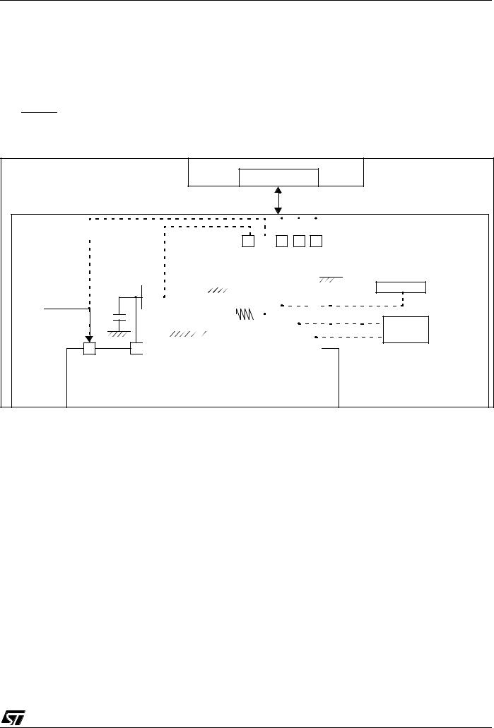
ST7262
FLASH PROGRAM MEMORY (Cont’d)
4.4 ICC Interface
ICC needs a minimum of 4 and up to 6 pins to be connected to the programming tool (see Figure 9). These pins are:
–RESET: device reset
–VSS: device power supply ground
–ICCCLK: ICC output serial clock pin
–ICCDATA: ICC input/output serial data pin
–ICCSEL/VPP: programming voltage
–OSC1(or OSCIN): main clock input for external source (optional)
–VDD: application board power supply (optional, see Figure 9, Note 3)
Figure 9. Typical ICC Interface
PROGRAMMING TOOL
ICC CONNECTOR
ICC Cable
APPLICATION BOARD
 OPTIONAL
 (See Note 3)
APPLICATION  CL2
CL2
POWER SUPPLY
|
|
|
|
|
|
|
|
|
|
|
|
|
|
OSC2 |
V |
|
|||
|
DD |
|
|
|
|
|
|
|
|
OPTIONAL |
|
|
|
|
|
|
|
|
|
|
|
|
|
|
|
|
|
|
|
|
|
|
||||||
|
|
|
|
|
(See Note 4) |
|
9 |
|
7 |
|
5 |
|
3 |
|
1 |
|
|
||||||||||||||||
|
|
|
|
|
|
|
|
|
|
|
|
|
|
|
|
|
|
|
|
|
|
|
|
|
|
|
|
|
|||||
|
|
|
|
|
|
|
|
|
|
|
|
|
|
|
|
|
10 |
|
8 |
|
6 |
|
4 |
|
2 |
|
|
||||||
|
|
|
|
|
|
|
|
|
|
|
|
|
|
|
|
|
|
|
|
|
|
|
|
|
|
|
|
|
|
|
|
|
|
|
|
|
|
|
|
|
|
|
|
|
|
|
|
|
|
|
|
|
|
|
|
|
|
|
|
|
|
|
|
|
|
|
|
|
|
|
|
|
|
|
|
CL1 |
|
|
|
|
|
10kΩ |
|
|
|
|
|
|
|
|
|
|
|
|
|
|
|||||
|
|
|
|
|
|
|
|
|
|
|
|
|
|
|
|
|
|
|
|
|
|
|
|
|
|
|
|||||||
|
|
|
|
|
|
|
|
|
|
|
|
|
|
|
|
|
|
|
|
|
|
|
|
|
|
|
|||||||
|
|
|
|
|
|
|
|
|
|
|
|
|
|
|
|
|
|
|
|
|
|
|
|
|
|
|
|||||||
|
|
|
|
|
|
|
|
|
|
|
|
|
|
|
|
|
|
|
|
|
|
|
|
|
|
|
|
|
|
|
|
|
|
|
|
|
|
|
|
|
|
|
|
|
|
|
|
|
|
|
|
|
|
|
|
|
|
|
|
|
|
|
|
|
|
||
|
|
|
|
|
|
|
|
|
|
|
|
|
|
|
|
|
|
|
|
|
|
|
|
|
|
|
|
|
|
|
|
||
|
|
|
|
|
|
|
|
|
|
|
|
|
|
|
|
|
|
|
|
|
|
|
|
|
|
|
|
|
|
|
|
|
|
|
|
|
|
|
|
|
|
|
|
|
|
|
|
|
|
|
|
|
|
|
|
|
|
|
|
|
|
|
|
|
|
|
|
|
|
|
|
|
|
|
|
|
|
|
|
|
|
|
|
|
|
|
|
|
|
|
|
|
|
|
|
|
|
|
|||
|
|
|
OSC1 |
V |
ICCSEL/VPP |
|
RESET |
|
ICCCLK |
|
|
ICCDATA |
|||||||||||||||||||||
|
|
|
|
|
|
|
|
|
|
|
|
|
SS |
|
|
|
|
|
|
|
|
|
|
|
|
|
|
||||||
|
|
|
|
|
|
|
|
ST7 |
|
|
|
|
|
|
|
|
|
|
|
|
|
|
|
|
|
|
|
|
|
|
|||
|
|
|
|
|
|
|
|
|
|
|
|
|
|
|
|
|
|
|
|
|
|
|
|
|
|
|
|||||||
ICC CONNECTOR
HE10 CONNECTOR TYPE
APPLICATION
RESET SOURCE
See Note 2
See Note 1
APPLICATION
I/O
Notes:
1.If the ICCCLK or ICCDATA pins are only used as outputs in the application, no signal isolation is necessary. As soon as the Programming Tool is plugged to the board, even if an ICC session is not in progress, the ICCCLK and ICCDATA pins are not available for the application. If they are used as inputs by the application, isolation such as a serial resistor has to implemented in case another device forces the signal. Refer to the Programming Tool documentation for recommended resistor values.
2.During the ICC session, the programming tool must control the RESET pin. This can lead to conflicts between the programming tool and the application reset circuit if it drives more than 5mA at high level (push pull output or pull-up resistor<1K). A schottky diode can be used to isolate the application RESET circuit in this case. When using a classical RC network with R>1K or a reset man-
agement IC with open drain output and pull-up resistor>1K, no additional components are needed. In all cases the user must ensure that no external reset is generated by the application during the ICC session.
3.The use of Pin 7 of the ICC connector depends on the Programming Tool architecture. This pin must be connected when using most ST Programming Tools (it is used to monitor the application power supply). Please refer to the Programming Tool manual.
4.Pin 9 has to be connected to the OSC1 or OSCIN pin of the ST7 when the clock is not available in the application or if the selected clock option is not programmed in the option byte. ST7 devices with multi-oscillator capability need to have OSC2 grounded in this case.
15/132

ST7262
FLASH PROGRAM MEMORY (Cont’d)
4.5 ICP (In-Circuit Programming)
To perform ICP the microcontroller must be switched to ICC (In-Circuit Communication) mode by an external controller or programming tool.
Depending on the ICP code downloaded in RAM, Flash memory programming can be fully customized (number of bytes to program, program locations, or selection serial communication interface for downloading).
When using an STMicroelectronics or third-party programming tool that supports ICP and the specific microcontroller device, the user needs only to implement the ICP hardware interface on the application board (see Figure 9). For more details on the pin locations, refer to the device pinout description.
4.6 IAP (In-Application Programming)
This mode uses a BootLoader program previously stored in Sector 0 by the user (in ICP mode or by plugging the device in a programming tool).
This mode is fully controlled by user software. This allows it to be adapted to the user application, (us- er-defined strategy for entering programming mode, choice of communications protocol used to fetch the data to be stored, etc.). For example, it is possible to download code from the SPI, SCI, USB or CAN interface and program it in the Flash. IAP mode can be used to program any of the Flash sectors except Sector 0, which is write/erase protected to allow recovery in case errors occur during the programming operation.
16/132
4.7 Related Documentation
For details on Flash programming and ICC protocol, refer to the ST7 Flash Programming Reference Manual and to the ST7 ICC Protocol Reference Manual.
4.8 Register Description
FLASH CONTROL/STATUS REGISTER (FCSR)
Read/Write
Reset Value: 0000 0000 (00h)
7 |
|
|
|
|
|
|
0 |
|
|
|
|
|
|
|
|
0 |
0 |
0 |
0 |
0 |
0 |
0 |
0 |
|
|
|
|
|
|
|
|
This register is reserved for use by Programming Tool software. It controls the Flash programming and erasing operations.

ST7262
5 CENTRAL PROCESSING UNIT
5.1 INTRODUCTION
This CPU has a full 8-bit architecture and contains six internal registers allowing efficient 8-bit data manipulation.
5.2 MAIN FEATURES
■Enable executing 63 basic instructions
■Fast 8-bit by 8-bit multiply
■17 main addressing modes (with indirect addressing mode)
■Two 8-bit index registers
■16-bit stack pointer
■Low power HALT and WAIT modes
■Priority maskable hardware interrupts
■Non-maskable software/hardware interrupts
5.3 CPU REGISTERS
The 6 CPU registers shown in Figure 10 are not present in the memory mapping and are accessed by specific instructions.
Accumulator (A)
The Accumulator is an 8-bit general purpose register used to hold operands and the results of the arithmetic and logic calculations and to manipulate data.
Index Registers (X and Y)
These 8-bit registers are used to create effective addresses or as temporary storage areas for data manipulation. (The Cross-Assembler generates a precede instruction (PRE) to indicate that the following instruction refers to the Y register.)
The Y register is not affected by the interrupt automatic procedures.
Program Counter (PC)
The program counter is a 16-bit register containing the address of the next instruction to be executed by the CPU. It is made of two 8-bit registers PCL (Program Counter Low which is the LSB) and PCH (Program Counter High which is the MSB).
Figure 10. CPU Registers
|
|
|
|
|
|
|
|
|
|
7 |
|
|
|
|
|
|
|
0 |
|
|
|
||
|
|
|
|
|
|
|
|
|
|
|
|
|
|
|
|
|
|
|
|
|
|
|
ACCUMULATOR |
|
|
|
|
|
|
|
|
|
|
|
|
RESET VALUE = XXh |
|
|
|
|
|||||||
|
|
|
|
|
|
|
|
|
|
7 |
|
|
|
|
|
|
|
0 |
|
|
|
||
|
|
|
|
|
|
|
|
|
|
|
|
|
|
|
|
|
|
|
|
|
|
|
X INDEX REGISTER |
|
|
|
|
|
|
|
|
|
|
|
|
|
|
|
|
|
|
|
|
|
|
|
|
|
|
|
|
|
|
|
|
|
|
|
|
|
|
|
|
|
|
|
|
|
|
|
|
|
|
|
|
|
|
|
|
|
|
|
RESET VALUE = XXh |
|
|
|
|
||||||||
|
|
|
|
|
|
|
|
|
|
7 |
|
|
|
|
|
|
|
0 |
|
|
|
||
|
|
|
|
|
|
|
|
|
|
|
|
|
|
|
|
|
|
|
|
|
|
|
Y INDEX REGISTER |
|
|
|
|
|
|
|
|
|
|
|
|
|
|
|
|
|
|
|
|
|
|
|
|
|
|
|
|
|
|
|
|
|
|
|
RESET VALUE = XXh |
|
|
|
|
||||||||
|
|
|
|
|
PCH |
8 |
|
7 |
|
|
PCL |
|
|
|
0 |
|
|
PROGRAM COUNTER |
|||||
|
15 |
|
|
|
|
|
|
|
|
|
|
||||||||||||
|
|
|
|
|
|
|
|
|
|
||||||||||||||
|
|
|
|
|
|
|
|
|
|
|
|
|
|
|
|
|
|
|
|
|
|
|
|
|
|
|
|
|
|
|
|
|
|
|
|
|
|
|
|
|
|
|
|
|
|
|
|
RESET VALUE = RESET VECTOR @ FFFEh-FFFFh |
|
||||||||||||||||||||||
|
|
|
|
|
|
|
|
|
|
7 |
|
|
|
|
|
|
|
0 |
|
|
|
||
|
|
|
|
|
|
|
|
|
|
|
|
|
|
|
|
|
|
|
|
|
|
|
|
|
|
|
|
|
|
|
|
|
|
|
|
1 |
1 |
I1 |
H |
I0 |
N |
|
Z |
C |
|
CONDITION CODE REGISTER |
|
|
|
|
|
|
|
|
|
|
|
|
|
|
|
|
|
|
|
|
|
|
|
|
|
|
|
|
|
RESET VALUE = 1 |
1 |
1 X |
1 |
X |
X |
X |
|
||||||||||||
|
|
15 |
|
|
|
|
|
8 |
|
|
|
|
|
|
|
|
0 |
|
|
STACK POINTER |
|||
|
|
|
|
|
|
|
7 |
|
|
|
|
|
|
|
|
|
|||||||
|
|
|
|
|
|
|
|
|
|
|
|
|
|
|
|
|
|
|
|
|
|
|
|
RESET VALUE = STACK HIGHER ADDRESS |
|
|
|
|
|
||||||||||||||||||
X = Undefined Value
17/132

ST7262
CENTRAL PROCESSING UNIT (Cont’d)
Condition Code Register (CC)
Read/Write
Reset Value: 111x1xxx
7 |
|
|
|
|
|
|
0 |
|
|
|
|
|
|
|
|
1 |
1 |
I1 |
H |
I0 |
N |
Z |
C |
|
|
|
|
|
|
|
|
The 8-bit Condition Code register contains the interrupt masks and four flags representative of the result of the instruction just executed. This register can also be handled by the PUSH and POP instructions.
These bits can be individually tested and/or controlled by specific instructions.
Arithmetic Management Bits
Bit 4 = H Half carry.
This bit is set by hardware when a carry occurs between bits 3 and 4 of the ALU during an ADD or ADC instructions. It is reset by hardware during the same instructions.
0:No half carry has occurred.
1:A half carry has occurred.
This bit is tested using the JRH or JRNH instruction. The H bit is useful in BCD arithmetic subroutines.
Bit 2 = N Negative.
This bit is set and cleared by hardware. It is representative of the result sign of the last arithmetic, logical or data manipulation. It’s a copy of the result 7th bit.
0:The result of the last operation is positive or null.
1:The result of the last operation is negative
(i.e. the most significant bit is a logic 1).
This bit is accessed by the JRMI and JRPL instructions.
Bit 1 = Z Zero.
18/132
This bit is set and cleared by hardware. This bit indicates that the result of the last arithmetic, logical or data manipulation is zero.
0:The result of the last operation is different from zero.
1:The result of the last operation is zero.
This bit is accessed by the JREQ and JRNE test instructions.
Bit 0 = C Carry/borrow.
This bit is set and cleared by hardware and software. It indicates an overflow or an underflow has occurred during the last arithmetic operation.
0:No overflow or underflow has occurred.
1:An overflow or underflow has occurred.
This bit is driven by the SCF and RCF instructions and tested by the JRC and JRNC instructions. It is also affected by the “bit test and branch”, shift and rotate instructions.
Interrupt Management Bits
Bit 5,3 = I1, I0 Interrupt
The combination of the I1 and I0 bits gives the current interrupt software priority.
Interrupt Software Priority |
I1 |
I0 |
|
|
|
|
|
Level 0 |
(main) |
1 |
0 |
|
|
|
|
Level 1 |
|
0 |
1 |
|
|
|
|
Level 2 |
|
0 |
0 |
|
|
|
|
Level 3 |
(= interrupt disable) |
1 |
1 |
|
|
|
|
These two bits are set/cleared by hardware when entering in interrupt. The loaded value is given by the corresponding bits in the interrupt software priority registers (IxSPR). They can be also set/ cleared by software with the RIM, SIM, IRET, HALT, WFI and PUSH/POP instructions.
See the interrupt management chapter for more details.
ST7262
CPU REGISTERS (Cont’d)
STACK POINTER (SP)
Read/Write
Reset Value: 017Fh
15 |
|
|
|
|
|
|
8 |
|
|
|
|
|
|
|
|
0 |
0 |
0 |
0 |
0 |
0 |
0 |
1 |
|
|
|
|
|
|
|
|
7 |
|
|
|
|
|
|
0 |
|
|
|
|
|
|
|
|
1 |
SP6 |
SP5 |
SP4 |
SP3 |
SP2 |
SP1 |
SP0 |
|
|
|
|
|
|
|
|
The Stack Pointer is a 16-bit register which is always pointing to the next free location in the stack. It is then decremented after data has been pushed onto the stack and incremented before data is popped from the stack (see Figure 11).
Since the stack is 128 bytes deep, the 9 most significant bits are forced by hardware. Following an MCU Reset, or after a Reset Stack Pointer instruction (RSP), the Stack Pointer contains its reset value (the SP6 to SP0 bits are set) which is the stack higher address.
The least significant byte of the Stack Pointer (called S) can be directly accessed by a LD instruction.
Note: When the lower limit is exceeded, the Stack Pointer wraps around to the stack upper limit, without indicating the stack overflow. The previously stored information is then overwritten and therefore lost. The stack also wraps in case of an underflow.
The stack is used to save the return address during a subroutine call and the CPU context during an interrupt. The user may also directly manipulate the stack by means of the PUSH and POP instructions. In the case of an interrupt, the PCL is stored at the first location pointed to by the SP. Then the other registers are stored in the next locations as shown in Figure 11.
–When an interrupt is received, the SP is decremented and the context is pushed on the stack.
–On return from interrupt, the SP is incremented and the context is popped from the stack.
A subroutine call occupies two locations and an interrupt five locations in the stack area.
Figure 11. Stack Manipulation Example
|
CALL |
Interrupt |
PUSH Y |
POP Y |
IRET |
RET |
|
Subroutine |
Event |
|
|
|
or RSP |
||
@ 0100h |
|
|
|
|
|
|
|
|
|
SP |
|
|
|
|
|
|
|
SP |
Y |
SP |
|
|
|
|
|
|
|
|
|
||
|
|
CC |
CC |
CC |
|
|
|
|
|
A |
A |
A |
|
|
|
|
|
X |
X |
X |
|
|
|
SP |
|
PCH |
PCH |
PCH |
SP |
|
|
|
PCL |
PCL |
PCL |
|
|||
|
|
|
|
||||
|
PCH |
PCH |
PCH |
PCH |
PCH |
SP |
|
@ 017Fh |
PCL |
PCL |
PCL |
PCL |
PCL |
||
|
|||||||
|
Stack Higher Address = 017Fh |
|
|
|
|
||
|
Stack Lower Address = 0100h |
|
|
|
|
||
|
|
|
|
|
|
19/132 |
|
ST7262
6 CLOCKS AND RESET
6.1 CLOCK SYSTEM
6.1.1 General Description
The MCU accepts either a Crystal or Ceramic resonator, or an external clock signal to drive the internal oscillator. The internal clock (fCPU) is derived from the external oscillator frequency (fOSC),
by dividing by 3 and multiplying by 2. By setting the OSC12/6 bit in the option byte, a 12 MHz external clock can be used giving an internal frequency of 8 MHz while maintaining a 6 MHz clock for USB (refer to Figure 14).
The internal clock signal (fCPU) consists of a square wave with a duty cycle of 50%.
It is further divided by 1, 2, 4 or 8 depending on the Slow Mode Selection bits in the Miscellaneous register (SMS[1:0])
The internal oscillator is designed to operate with an AT-cut parallel resonant quartz or ceramic resonator in the frequency range specified for fosc.
The circuit shown in Figure 13 is recommended when using a crystal, and Table 4 lists the recommended capacitors. The crystal and associated components should be mounted as close as possible to the input pins in order to minimize output distortion and start-up stabilization time.
Table 4. Recommended |
Values for |
12 MHz |
|||
Crystal Resonator |
|
|
|
||
|
|
|
|
|
|
RSMAX |
20 Ω |
|
25 Ω |
|
70 Ω |
COSCIN |
56pF |
|
47pF |
|
22pF |
COSCOUT |
56pF |
|
47pF |
|
22pF |
RP |
1-10 MΩ |
|
1-10 MΩ |
|
1-10 MΩ |
Note: RSMAX is the equivalent serial resistor of the crystal (see crystal specification).
6.1.2 External Clock input
An external clock may be applied to the OSCIN input with the OSCOUT pin not connected, as shown on Figure 12. The tOXOV specifications does not apply when using an external clock input. The equivalent specification of the external clock
source should be used instead of tOXOV (see Electrical Characteristics).
6.1.3 Clock Output Pin (MCO)
The internal clock (fCPU) can be output on Port B0 by setting the MCO bit in the Miscellaneous regis-
ter.
20/132
Figure 12. External Clock Source Connections
OSCIN OSCOUT
NC
EXTERNAL
CLOCK
Figure 13. Crystal/Ceramic Resonator
OSCIN OSCOUT
|
|
|
|
|
|
|
|
|
|
|
|
|
|
|
|
|
|
COSCIN |
|
|
|
|
|
|
|
|
|
|
|
|
|
|
COSCOUT |
||
|
|
|
|
|
|
|
|
|
|
|
|
|
|
||||
|
|
|
|
|
|
|
|
|
|
|
|
|
|
||||
|
|
|
|
|
|
|
|
|
|
|
|
|
|
||||
|
|
|
|
|
|
|
|
|
|
|
|
|
|
||||
|
|
|
|
|
|
|
|
|
|
|
|
|
|
|
|
|
|
|
|
|
|
|
|
|
|
|
|
|
|
|
|
|
|
|
|
Figure 14. Clock block diagram
|
|
Slow |
fCPU 8/4/2/1 MHz |
|
|
Mode |
(or 4/2/1/0.5 MHz) |
|
|
% |
to CPU and |
|
|
1/2/4/8 |
|
|
|
peripherals |
|
x2 |
|
SMS[1:0] |
|
|
|
|
|
%3 |
|
|
|
|
|
OSC12/6 |
MCO pin |
|
|
|
|
|
|
0 |
|
12 or |
|
|
6 MHz (USB) |
|
1 |
|
|
6 MHz |
%2 |
|
|
Crystal |
|
|
|
|
|
|
ST7262
6.2 RESET
The Reset procedure is used to provide an orderly software start-up or to exit low power modes.
Three reset modes are provided: a low voltage re- set, a watchdog reset and an external reset at the RESET pin.
A reset causes the reset vector to be fetched from addresses FFFEh and FFFFh in order to be loaded into the PC and with program execution starting from this point.
An internal circuitry provides a 514 CPU clock cycle delay from the time that the oscillator becomes active.
6.2.1 Low Voltage Reset
Low voltage reset circuitry generates a reset when VDD is:
■below VIT+ when VDD is rising,
■below VIT- when VDD is falling.
During low voltage reset, the RESET pin is held low, thus permitting the MCU to reset other devices.
The Low Voltage Detector can be disabled by setting the LVD bit of the Option byte.
6.2.2 Watchdog Reset
When a watchdog reset occurs, the RESET pin is pulled low permitting the MCU to reset other devices as when low voltage reset (Figure 15).
6.2.3 External Reset
The external reset is an active low input signal applied to the RESET pin of the MCU.
As shown in Figure 18, the RESET signal must stay low for a minimum of one and a half CPU clock cycles.
An internal Schmitt trigger at the RESET pin is provided to improve noise immunity.
Figure 15. Low Voltage Reset functional Diagram
RESET |
LOW VOLTAGE |
VDD |
RESET |
INTERNAL |
RESET |
FROM |
WATCHDOG |
RESET |
Figure 16. Low Voltage Reset Signal Output
VIT+ |
VIT- |
VDD |
RESET |
Note: Typical hysteresis (VIT+-VIT-) of 250 mV is expected
Figure 17. Temporization Timing Diagram after an internal Reset
VDD |
VIT+ |
|
|
|
Temporization |
|
(514 CPU clock cycles) |
Addresses |
$FFFE |
|
21/132
ST7262
Figure 18. Reset Timing Diagram
|
tDDR |
|
VDD |
|
|
OSCIN |
|
|
|
tOXOV |
|
fCPU |
|
|
PC |
FFFE |
FFFF |
RESET |
514 CPU |
|
|
|
|
|
CLOCK |
|
|
CYCLES |
|
|
DELAY |
|
Note: Refer to Electrical Characteristics for values of tDDR, tOXOV, VIT+ and VIT-.
Figure 19. Reset Block Diagram
|
|
|
|
|
|
|
|
VDD |
|
|
|
|
|
|
|
|
|
|
|||||||||
|
|
|
|
|
|
|
|
|
|
|
|
|
|
|
|
||||||||||||
|
|
|
|
|
|
|
|
|
|
|
RON |
|
|
|
|
|
|
|
|
|
|
||||||
|
|
|
|
|
|
|
|
|
|
|
|
|
|
|
|
|
|
|
|
|
|||||||
|
|
|
|
|
|
|
|
|
|
|
|
|
|
|
|
200ns |
|
|
|
|
|
|
|
|
|
|
INTERNAL |
|
RESET |
|
|
|
|
|
|
|
|
|
|
|
|
|
|||||||||||||
|
|
|
|
|
|
|
|
|
|
|
|
|
|
Filter |
|
|
|
|
|
|
|
|
|
|
RESET |
||
|
|
|
|
|
|
|
|
|
|
|
|
|
|
|
|
|
|
|
|
|
|
|
|
|
|
||
|
|
|
|
|
|
|
|
|
|
|
|
|
|
|
|
|
|
|
|
|
|
|
|
|
|
|
WATCHDOG RESET |
|
|
|
|
|
|
|
|
|
|
|
|
|
|
|
|
|
|
|
|
|
|
|
|
|
|
|
|
|
|
|
|
|
|
|
|
|
|
|
|
|
|
|
tw(RSTL)out + 128 fOSC |
|
|
|
PULSE |
|
|||||||
|
|
|
|
|
|
|
|
|
|
|
|
|
|
|
delay |
|
|
GENERATOR |
|
|
|
|
|||||
|
|
|
|
|
|
|
|
|
|
|
|
|
|
|
|
|
|
|
|
|
|
|
|
|
|
|
LVD RESET |
|
|
|
|
|
|
|
|
|
|
|
|
|
|
|
|
|
|
|
|
|
|
|
|
|
|
|
|
|
|
|
|
|
|
|
|
|
|
|
|
|
|
|
|
|
|
|
|
|
|
|
|
|
|
|
|
|
|
|
|
|
|
|
|
|
|
|
|
|
|
|
|
|
|
|
|
|
|
|
|
|
|
|
|
Note: The output of the external reset circuit must have an open-drain output to drive the ST7 reset pad. Otherwise the device can be damaged when the ST7 generates an internal reset (LVD or watchdog).
22/132
ST7262
7 INTERRUPTS
7.1 INTRODUCTION
The CPU enhanced interrupt management provides the following features:
■Hardware interrupts
■Software interrupt (TRAP)
■Nested or concurrent interrupt management with flexible interrupt priority and level management:
–Up to 4 software programmable nesting levels
–Up to 16 interrupt vectors fixed by hardware
–3 non maskable events: RESET, TRAP, TLI This interrupt management is based on:
–Bit 5 and bit 3 of the CPU CC register (I1:0),
–Interrupt software priority registers (ISPRx),
–Fixed interrupt vector addresses located at the high addresses of the memory map (FFE0h to FFFFh) sorted by hardware priority order.
This enhanced interrupt controller guarantees full upward compatibility with the standard (not nested) CPU interrupt controller.
7.2 MASKING AND PROCESSING FLOW
The interrupt masking is managed by the I1 and I0 bits of the CC register and the ISPRx registers which give the interrupt software priority level of each interrupt vector (see Table 5). The processing flow is shown in Figure 20.
When an interrupt request has to be serviced:
–Normal processing is suspended at the end of the current instruction execution.
–The PC, X, A and CC registers are saved onto the stack.
–I1 and I0 bits of CC register are set according to the corresponding values in the ISPRx registers of the serviced interrupt vector.
–The PC is then loaded with the interrupt vector of the interrupt to service and the first instruction of the interrupt service routine is fetched (refer to “Interrupt Mapping” table for vector addresses).
The interrupt service routine should end with the IRET instruction which causes the contents of the saved registers to be recovered from the stack.
Note: As a consequence of the IRET instruction, the I1 and I0 bits will be restored from the stack and the program in the previous level will resume.
Table 5. Interrupt Software Priority Levels
Interrupt software priority |
Level |
I1 |
I0 |
|||
|
|
|
|
|
|
|
Level 0 |
(main) |
Low |
1 |
0 |
||
|
|
|
|
|
|
|
Level 1 |
|
|
|
|
0 |
1 |
|
|
|
|
|
|
|
Level 2 |
|
|
|
|
0 |
0 |
|
|
|
|
|
|
|
Level 3 |
(= interrupt disable) |
High |
|
1 |
1 |
|
|
|
|
|
|
|
|
Figure 20. Interrupt Processing Flowchart
RESET |
PENDING |
Y |
|
|
TLI |
Y |
INTERRUPT |
|
|
|
|
||
|
|
|
|
|
|
|
|
N |
|
Interrupt has the same or a |
|
N |
|
|
|
lower software priority |
|
|
|
|
|
|
|
than current one |
|
I1:0 |
|
|
|
|
|
|
|
|
|
FETCH NEXT |
|
THE INTERRUPT |
|
|
|
|
INSTRUCTION |
|
STAYS PENDING |
|
|
|
|
Y |
|
Interrupt hashighera |
softwarepriority |
than currentone |
|
|
“IRET” |
|
|
|||
|
N |
|
|
|||
|
|
|
|
|||
RESTORE PC, X, A, CC |
EXECUTE |
|
|
|
|
|
FROM STACK |
INSTRUCTION |
|
STACK PC, X, A, CC |
|
||
|
|
|
LOAD I1:0 FROM INTERRUPT SW REG. |
|||
|
|
|
LOAD PC FROM INTERRUPT VECTOR |
|
||
|
|
|
|
|
|
23/132 |
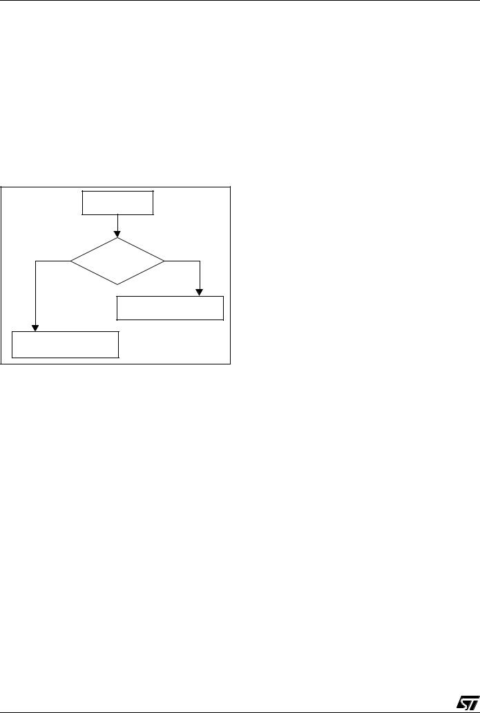
ST7262
INTERRUPTS (Cont’d)
Servicing Pending Interrupts
As several interrupts can be pending at the same time, the interrupt to be taken into account is determined by the following two-step process:
–the highest software priority interrupt is serviced,
–if several interrupts have the same software priority then the interrupt with the highest hardware priority is serviced first.
Figure 21 describes this decision process.
Figure 21. Priority Decision Process
|
PENDING |
|
|
INTERRUPTS |
|
Same |
SOFTWARE |
Different |
|
PRIORITY |
|
|
HIGHEST SOFTWARE |
|
|
PRIORITY SERVICED |
|
HIGHEST HARDWARE |
|
|
PRIORITY SERVICED |
|
|
When an interrupt request is not serviced immediately, it is latched and then processed when its software priority combined with the hardware priority becomes the highest one.
Note 1: The hardware priority is exclusive while the software one is not. This allows the previous process to succeed with only one interrupt.
Note 2: RESET, TRAP and TLI can be considered as having the highest software priority in the decision process.
Different Interrupt Vector Sources
Two interrupt source types are managed by the CPU interrupt controller: the non-maskable type (RESET, TLI, TRAP) and the maskable type (external or from internal peripherals).
Non-Maskable Sources
These sources are processed regardless of the state of the I1 and I0 bits of the CC register (see Figure 20). After stacking the PC, X, A and CC registers (except for RESET), the corresponding vector is loaded in the PC register and the I1 and I0 bits of the CC are set to disable interrupts (level 3). These sources allow the processor to exit HALT mode.
24/132
■ TLI (Top Level Hardware Interrupt)
This hardware interrupt occurs when a specific edge is detected on the dedicated TLI pin. Caution: A TRAP instruction must not be used in a TLI service routine.
■ TRAP (Non Maskable Software Interrupt)
This software interrupt is serviced when the TRAP instruction is executed. It will be serviced according to the flowchart in Figure 20 as a TLI.
Caution: TRAP can be interrupted by a TLI. ■ RESET
The RESET source has the highest priority in the CPU. This means that the first current routine has the highest software priority (level 3) and the highest hardware priority.
See the RESET chapter for more details.
Maskable Sources
Maskable interrupt vector sources can be serviced if the corresponding interrupt is enabled and if its own interrupt software priority (in ISPRx registers) is higher than the one currently being serviced (I1 and I0 in CC register). If any of these two conditions is false, the interrupt is latched and thus remains pending.
■ External Interrupts
External interrupts allow the processor to exit from HALT low power mode.
External interrupt sensitivity is software selectable through the ITRFRE2 register.
External interrupt triggered on edge will be latched and the interrupt request automatically cleared upon entering the interrupt service routine.
If several input pins of a group connected to the same interrupt line are selected simultaneously, these will be logically NANDed.
■ Peripheral Interrupts
Usually the peripheral interrupts cause the Device to exit from HALT mode except those mentioned in the “Interrupt Mapping” table.
A peripheral interrupt occurs when a specific flag is set in the peripheral status registers and if the corresponding enable bit is set in the peripheral control register.
The general sequence for clearing an interrupt is based on an access to the status register followed by a read or write to an associated register.
Note: The clearing sequence resets the internal latch. A pending interrupt (i.e. waiting for being serviced) will therefore be lost if the clear sequence is executed.

ST7262
INTERRUPTS (Cont’d)
7.3 INTERRUPTS AND LOW POWER MODES
All interrupts allow the processor to exit the WAIT low power mode. On the contrary, only external and other specified interrupts allow the processor to exit from the HALT modes (see column “Exit from HALT” in “Interrupt Mapping” table). When several pending interrupts are present while exiting HALT mode, the first one serviced can only be an interrupt with exit from HALT mode capability and it is selected through the same decision process shown in Figure 21.
Note: If an interrupt, that is not able to Exit from HALT mode, is pending with the highest priority when exiting HALT mode, this interrupt is serviced after the first one serviced.
Figure 22. Concurrent Interrupt Management
7.4 CONCURRENT & NESTED MANAGEMENT
The following Figure 22 and Figure 23 show two different interrupt management modes. The first is called concurrent mode and does not allow an interrupt to be interrupted, unlike the nested mode in Figure 23. The interrupt hardware priority is given in this order from the lowest to the highest: MAIN, IT4, IT3, IT2, IT1, IT0, TLI. The software priority is given for each interrupt.
Warning: A stack overflow may occur without notifying the software of the failure.
HARDWARE PRIORITY
|
IT2 |
IT1 |
IT4 |
IT3 |
TLI |
IT0 |
SOFTWARE |
|
|
I1 |
|
|
|
|
|
|
I0 |
|||||||
|
PRIORITY |
|
|
|
|
|
|
|
||||||||||||||||
|
|
|
|
|
|
|
|
|
|
|
|
|
|
|
|
|
|
|
|
|
|
|
||
|
|
|
|
|
|
|
|
|
|
|
|
|
LEVEL |
|
|
|
|
|
|
|
|
|
BYTES |
|
|
|
|
|
|
|
|
|
|
|
|
|
IT0 |
|
|
3 |
|
1 |
|
1 |
|||||
|
|
|
|
|
|
|
|
|
|
|
TLI |
|
|
3 |
|
1 |
|
1 |
|
|||||
|
|
|
|
|
|
|
IT1 |
|
|
|
IT1 |
|
|
3 |
|
1 |
|
1 |
= 10 |
|||||
|
|
|
IT2 |
|
|
|
|
|
|
|
|
|
|
3 |
|
1 |
|
1 |
STACK |
|||||
|
|
|
|
|
|
|
|
|
|
|
|
|
|
|
|
|||||||||
RIM |
|
|
|
|
|
|
|
|
|
IT3 |
|
|
3 |
|
1 |
|
1 |
USED |
||||||
|
|
|
|
|
|
|
|
|
|
|
|
3 |
|
1 |
|
1 |
||||||||
|
|
|
|
|
|
|
|
|
|
|
|
|
|
|
||||||||||
|
|
|
|
|
|
|
|
|
|
|
|
IT4 |
|
|
|
|
|
|||||||
MAIN |
|
|
|
|
|
|
|
|
|
|
MAIN |
3/0 |
|
|
|
|
|
|
|
|
||||
|
|
|
|
|
|
|
|
|
|
|
|
|
|
|
|
|
|
|||||||
11 / 10 |
|
|
|
|
|
|
|
|
|
|
|
10 |
|
|
|
|
|
|
|
|
|
|
|
|
|
|
|
|
|
|
|
|
|
|
|
|
|
|
|
|
|
|
|
|
|
|
|||
Figure 23. Nested Interrupt Management
HARDWARE PRIORITY
IT2 |
IT1 |
IT4 |
IT3 |
TLI |
IT0 |
SOFTWARE |
|
I1 |
|
|
|
I0 |
||||||
PRIORITY |
|
|
|
|
||||||||||||||
|
|
|
|
|
|
|
|
|
|
|
|
LEVEL |
|
|
|
|
|
|
|
|
|
|
|
|
|
|
|
|
|
|
|
|
|
|
|
|
|
|
|
|
|
|
|
|
|
|
|
|
|
|
|
|
|
|
|
|
|
|
TLI |
|
3 |
1 |
1 |
||
|
|
IT0 |
|
3 |
1 |
1 |
||
|
IT1 |
|
IT1 |
2 |
0 |
0 |
||
|
IT2 |
|
IT2 |
1 |
0 |
1 |
||
RIM |
IT3 |
|
3 |
1 |
1 |
|||
|
|
3 |
1 |
1 |
||||
|
IT4 |
IT4 |
|
|||||
MAIN |
|
MAIN |
3/0 |
|
|
|
|
|
|
|
|
|
|
||||
11 / 10 |
|
10 |
|
|
|
|
|
|
|
|
|
|
|
|
|||
USED STACK = 20 BYTES
25/132
ST7262
INTERRUPTS (Cont’d)
7.5 INTERRUPT REGISTER DESCRIPTION CPU CC REGISTER INTERRUPT BITS
Read/Write
Reset Value: 111x 1010 (xAh)
7 |
|
|
|
|
|
|
0 |
1 |
1 |
I1 |
H |
I0 |
N |
Z |
C |
|
|
|
|
|
|
|
|
Bit 5, 3 = I1, I0 Software Interrupt Priority
These two bits indicate the current interrupt software priority.
Interrupt Software Priority |
Level |
I1 |
I0 |
|
Level 0 |
(main) |
Low |
1 |
0 |
Level 1 |
|
|
0 |
1 |
Level 2 |
|
|
0 |
0 |
Level 3 |
(= interrupt disable*) |
High |
1 |
1 |
These two bits are set/cleared by hardware when entering in interrupt. The loaded value is given by the corresponding bits in the interrupt software priority registers (ISPRx).
They can be also set/cleared by software with the RIM, SIM, HALT, WFI, IRET and PUSH/POP instructions (see “Interrupt Dedicated Instruction Set” table).
*Note: TLI, TRAP and RESET events can interrupt a level 3 program.
INTERRUPT SOFTWARE PRIORITY REGISTERS (ISPRX)
Read/Write (bit 7:4 of ISPR3 are read only)
Reset Value: 1111 1111 (FFh)
|
7 |
|
|
|
|
|
|
0 |
|
|
|
|
|
|
|
|
|
ISPR0 |
I1_3 |
I0_3 |
I1_2 |
I0_2 |
I1_1 |
I0_1 |
I1_0 |
I0_0 |
|
|
|
|
|
|
|
|
|
ISPR1 |
I1_7 |
I0_7 |
I1_6 |
I0_6 |
I1_5 |
I0_5 |
I1_4 |
I0_4 |
|
|
|
|
|
|
|
|
|
ISPR2 |
I1_11 |
I0_11 |
I1_10 |
I0_10 |
I1_9 |
I0_9 |
I1_8 |
I0_8 |
|
|
|
|
|
|
|
|
|
ISPR3 |
1 |
1 |
1 |
1 |
I1_13 |
I0_13 |
I1_12 |
I0_12 |
|
|
|
|
|
|
|
|
|
These four registers contain the interrupt software priority of each interrupt vector.
–Each interrupt vector (except RESET and TRAP) has corresponding bits in these registers where its own software priority is stored. This correspondance is shown in the following table.
Vector address |
ISPRx bits |
|
|
FFFBh-FFFAh |
I1_0 and I0_0 bits* |
|
|
FFF9h-FFF8h |
I1_1 and I0_1 bits |
|
|
... |
... |
|
|
FFE1h-FFE0h |
I1_13 and I0_13 bits |
|
|
–Each I1_x and I0_x bit value in the ISPRx registers has the same meaning as the I1 and I0 bits in the CC register.
–Level 0 can not be written (I1_x=1, I0_x=0). In this case, the previously stored value is kept. (example: previous=CFh, write=64h, result=44h)
The RESET, TRAP and TLI vectors have no software priorities. When one is serviced, the I1 and I0 bits of the CC register are both set.
*Note: Bits in the ISPRx registers which correspond to the TLI can be read and written but they are not significant in the interrupt process management.
Caution: If the I1_x and I0_x bits are modified while the interrupt x is executed the following behaviour has to be considered: If the interrupt x is still pending (new interrupt or flag not cleared) and the new software priority is higher than the previous one, the interrupt x is re-entered. Otherwise, the software priority stays unchanged up to the next interrupt request (after the IRET of the interrupt x).
26/132
ST7262
7.6 Interrupt Register
INTERRUPT REGISTER 1 (ITRFRE1)
Address: 0008h - Read/Write
Reset Value: 0000 0000 (00h)
7 |
0 |
IT8E IT7E IT6E IT5E IT4E IT3E IT2E IT1E
Bit 7:0 = ITiE Interrupt Enable
0:I/O pin free for general purpose I/O
1:ITi external interrupt enabled.
Note: The corresponding interrupt is generated when:
–a rising edge occurs on the IT5/IT6 pins
–a falling edge occurs on the IT1, 2, 3, 4, 7 and 8 pins
INTERRUPT REGISTER 2 (ITRFRE2)
Address: 0039h - Read/Write
Reset Value: 0000 0000 (00h)
7 |
0 |
CTL3 CTL2 CTL1 CTL0 IT12E IT11E IT10E IT9E
Bit 5:4 = CTL[1:0] IT[10:9]1nterrupt Sensitivity
These bits are set and cleared by software. They are used to configure the edge and level sensitivity of the IT10 and IT9 external interrupt pins (this means that both must have the same sensitivity).
CTL1 |
CTL0 |
IT[10:9] Sensitivity |
|
|
|
0 |
0 |
Falling edge and low level |
|
|
|
0 |
1 |
Rising edge only |
|
|
|
1 |
0 |
Falling edge only |
|
|
|
1 |
1 |
Rising and falling edge |
|
|
|
Bit 3:0 = ITiE Interrupt Enable
0:I/O pin free for general purpose I/O
1:ITi external interrupt enabled.
Bit 7:6 = CTL[3:2] IT[12:11] Interrupt Sensitivity
These bits are set and cleared by software. They are used to configure the edge and level sensitivity of the IT12 and IT11 external interrupt pins (this means that both must have the same sensitivity).
CTL3 |
CTL2 |
IT[12:11] Sensitivity |
|
|
|
0 |
0 |
Falling edge and low level |
|
|
|
0 |
1 |
Rising edge only |
|
|
|
1 |
0 |
Falling edge only |
|
|
|
1 |
1 |
Rising and falling edge |
|
|
|
27/132

ST7262
INTERRUPTS (Cont’d)
Table 6. Interrupt Mapping
|
Source |
|
Register |
Priority |
Exit |
Address |
||
N° |
Description |
from |
||||||
Block |
Label |
Order |
Vector |
|||||
|
|
HALT |
||||||
|
|
|
|
|
|
|
||
|
|
|
|
|
|
|
|
|
|
|
Reset |
|
Highest |
Yes |
FFFEh-FFFFh |
||
|
|
|
|
|
|
|||
|
|
TRAP software interrupt |
|
Priority |
No |
FFFCh-FFFDh |
||
|
|
|
|
|
|
|
|
|
0 |
ICP |
FLASH Start programming NMI interrupt |
|
|
|
Yes |
FFFAh-FFFBh |
|
|
|
|
|
|
|
|
|
|
1 |
USB |
USB End Suspend interrupt |
USBISTR |
|
|
Yes |
FFF8h-FFF9h |
|
|
|
|
|
|
|
|
|
|
2 |
|
Port A external interrupts IT[4:1] |
ITRFRE1 |
|
|
Yes |
FFF6h-FFF7h |
|
|
|
|
|
|
|
|
|
|
3 |
I/O Ports |
Port B external interrupts IT[8:5] |
ITRFRE1 |
|
|
Yes |
FFF4h-FFF5h |
|
|
|
|
|
|
|
|
|
|
4 |
|
Port C external interrupts IT[12:9] |
ITRFRE2 |
|
|
Yes |
FFF2h-FFF3h |
|
|
|
|
|
|
|
|
|
|
5 |
TBU |
Timebase Unit interrupt |
TBUCSR |
|
|
No |
FFF0h-FFF1h |
|
|
|
|
|
|
|
|
|
|
6 |
ART |
ART/PWM Timer interrupt |
ICCSR |
|
|
Yes |
FFEEh-FFEFh |
|
|
|
|
|
|
|
|
|
|
7 |
SPI |
SPI interrupt vector |
SPISR |
|
|
Yes |
FFECh-FFEDh |
|
|
|
|||||||
|
|
|
|
|
|
|
|
|
8 |
SCI |
SCI interrupt vector |
SCISR |
|
|
No |
FFEAh-FFEBh |
|
|
|
|
|
Lowest |
|
|
||
9 |
USB |
USB interrupt vector |
USBISTR |
No |
FFE8h-FFE9h |
|||
|
|
|
|
Priority |
|
|
||
10 |
ADC |
A/D End of conversion interrupt |
ADCCSR |
No |
FFE6h-FFE7h |
|||
|
|
|||||||
|
|
|
|
|
|
|
|
|
|
|
Reserved area |
|
|
|
|
FFE0h-FFE5h |
|
|
|
|
|
|
|
|
|
|
Table 7. Nested Interrupts Register Map and Reset Values
Address |
Register |
7 |
|
6 |
5 |
|
4 |
|
3 |
|
2 |
1 |
|
0 |
(Hex.) |
Label |
|
|
|
|
|
||||||||
|
|
|
|
|
|
|
|
|
|
|
|
|
||
|
|
|
|
|
|
|
|
|
|
|
||||
|
|
Ext. Interrupt Port B |
Ext. Interrupt Port A |
USB END SUSP |
Not Used |
|||||||||
0032h |
ISPR0 |
|
|
|
|
|
|
|
|
|
|
|
|
|
I1_3 |
|
I0_3 |
I1_2 |
|
I0_2 |
I1_1 |
|
I0_1 |
|
|
|
|||
|
Reset Value |
1 |
|
1 |
1 |
|
1 |
|
1 |
|
1 |
1 |
|
1 |
|
|
|
|
|
|
|
|
|
|
|
|
|
|
|
|
|
|
SPI |
|
ART |
|
TBU |
Ext. Interrupt Port C |
||||||
0033h |
ISPR1 |
|
|
|
|
|
|
|
|
|
|
|
|
|
I1_7 |
|
I0_7 |
I1_6 |
|
I0_6 |
I1_5 |
|
I0_5 |
I1_4 |
|
I0_4 |
|||
|
Reset Value |
1 |
|
1 |
1 |
|
1 |
|
1 |
|
1 |
1 |
|
1 |
|
|
|
|
|
|
|
|
|
|
|
|
|
|
|
|
|
Not Used |
|
ADC |
|
USB |
|
SCI |
||||||
0034h |
ISPR2 |
|
|
|
|
|
|
|
|
|
|
|
|
|
I1_11 |
|
I0_11 |
I1_10 |
|
I0_10 |
I1_9 |
|
I0_9 |
I1_8 |
|
I0_8 |
|||
|
Reset Value |
1 |
|
1 |
1 |
|
1 |
|
1 |
|
1 |
1 |
|
1 |
|
|
|
|
|
|
|
|
|
|
|
|
|
||
|
|
|
|
|
|
|
|
|
Not Used |
Not Used |
||||
0035h |
ISPR3 |
|
|
|
|
|
|
|
|
|
|
|
|
|
|
|
|
|
|
|
|
I1_13 |
|
I0_13 |
I1_12 |
|
I0_12 |
||
|
Reset Value |
1 |
|
1 |
1 |
|
1 |
|
1 |
|
1 |
1 |
|
1 |
|
|
|
|
|
|
|
|
|
|
|
|
|
|
|
28/132
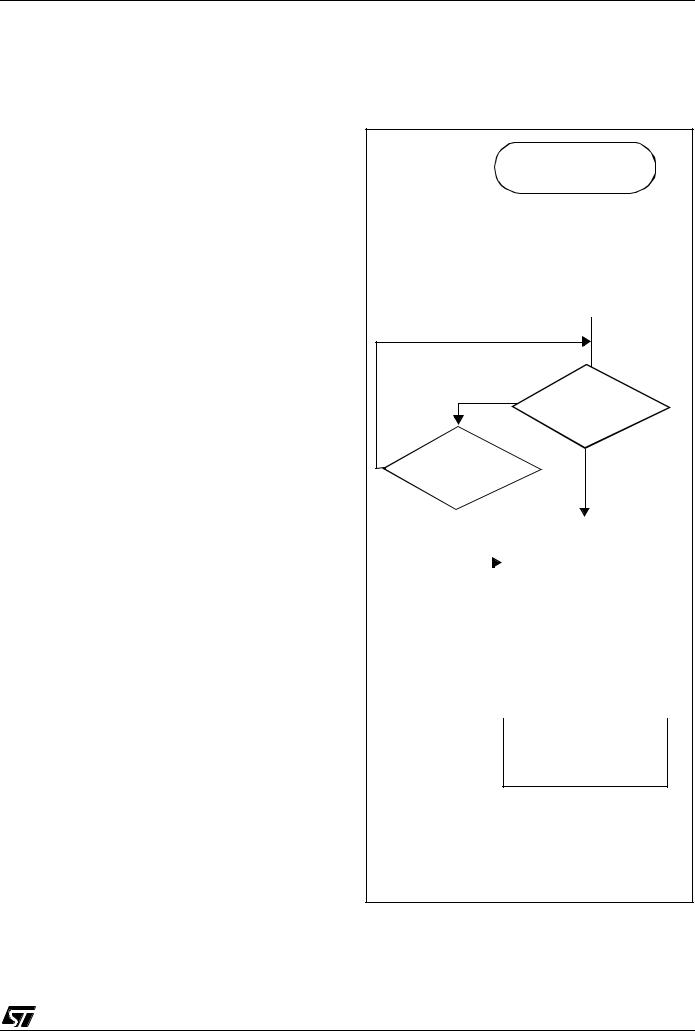
ST7262
8 POWER SAVING MODES
8.1 INTRODUCTION
There are three Power Saving modes. Slow Mode is selected by setting the SMS bits in the Miscellaneous register. Wait and Halt modes may be entered using the WFI and HALT instructions.
After a RESET the normal operating mode is selected by default (RUN mode). This mode drives the device (CPU and embedded peripherals) by means of a master clock which is based on the main oscillator frequency divided by 3 and multiplied by 2 (fCPU).
From Run mode, the different power saving modes may be selected by setting the relevant register bits or by calling the specific ST7 software instruction whose action depends on the oscillator status.
8.1.1 Slow Mode
In Slow mode, the oscillator frequency can be divided by a value defined in the Miscellaneous Register. The CPU and peripherals are clocked at this lower frequency. Slow mode is used to reduce power consumption, and enables the user to adapt clock frequency to available supply voltage.
8.2 WAIT MODE
WAIT mode places the MCU in a low power consumption mode by stopping the CPU.
This power saving mode is selected by calling the “WFI” ST7 software instruction.
All peripherals remain active. During WAIT mode, the I bit of the CC register is forced to 0, to enable all interrupts. All other registers and memory remain unchanged. The MCU remains in WAIT mode until an interrupt or Reset occurs, whereupon the Program Counter branches to the starting address of the interrupt or Reset service routine.
The MCU will remain in WAIT mode until a Reset or an Interrupt occurs, causing it to wake up.
Refer to Figure 24.
Figure 24. WAIT Mode Flow Chart
WFI INSTRUCTION
|
|
|
OSCILLATOR |
ON |
|
PERIPH. CLOCK |
ON |
|
CPU CLOCK |
OFF |
|
I-BIT |
CLEARED |
|
|
|
|
N |
RESET |
N |
Y |
INTERRUPT |
Y |
|
|
|
|
|
OSCILLATOR |
ON |
||
|
|
|||
|
|
PERIPH. CLOCK |
ON |
|
|
|
CPU CLOCK |
ON |
|
|
|
|||
|
|
I-BIT |
SET |
|
|
|
|
|
|
|
|
|
|
|
|
|
IF RESET |
|
|
|
|
514 CPU CLOCK |
||
|
|
CYCLES DELAY |
|
|
|
|
|
|
|
|
|
|
|
|
FETCH RESET VECTOR
OR SERVICE INTERRUPT
Note: Before servicing an interrupt, the CC register is pushed on the stack. The I-Bit is set during the interrupt routine and cleared when the CC register is popped.
29/132
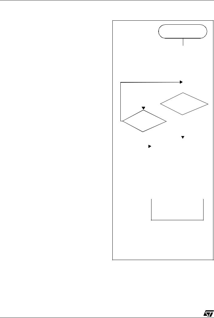
ST7262
POWER SAVING MODES (Cont’d)
8.3 HALT MODE
The HALT mode is the MCU lowest power consumption mode. The HALT mode is entered by executing the HALT instruction. The internal oscillator is then turned off, causing all internal processing to be stopped, including the operation of the on-chip peripherals.
When entering HALT mode, the I bit in the Condition Code Register is cleared. Thus, any of the external interrupts (ITi or USB end suspend mode), are allowed and if an interrupt occurs, the CPU clock becomes active.
The MCU can exit HALT mode on reception of either an external interrupt on ITi, an end suspend mode interrupt coming from USB peripheral, or a reset. The oscillator is then turned on and a stabilization time is provided before releasing CPU operation. The stabilization time is 514 CPU clock cycles.
After the start up delay, the CPU continues operation by servicing the interrupt which wakes it up or by fetching the reset vector if a reset wakes it up.
30/132
Figure 25. HALT Mode Flow Chart
HALT INSTRUCTION
OSCILLATOR |
OFF |
|
PERIPH. CLOCK |
OFF |
|
CPU CLOCK |
OFF |
|
I-BIT |
CLEARED |
|
|
|
|
|
|
|
N
|
|
|
|
|
|
RESET |
|
|
||
|
|
|
|
|
|
|
|
|||
N |
|
|
|
|
|
|||||
EXTERNAL |
|
|
Y |
|
|
|||||
INTERRUPT* |
|
|
|
|
||||||
|
|
|
|
|
||||||
|
|
Y |
|
|
|
|
|
|||
|
|
|
|
|
|
|
||||
|
|
|
|
|
||||||
|
|
|
|
OSCILLATOR |
ON |
|
||||
|
|
|
|
PERIPH. CLOCK |
ON |
|
||||
|
|
|
|
|
||||||
|
|
|
|
CPU CLOCK |
ON |
|
||||
|
|
|
|
I-BIT |
|
|
|
SET |
|
|
|
|
|
|
|
|
|
|
|
||
|
|
|
|
|
|
|
|
|
||
|
|
|
|
|
|
514 CPU CLOCK |
|
|||
|
|
|
|
|
|
CYCLES DELAY |
|
|||
|
|
|
|
|
|
|
|
|
|
|
|
|
|
|
|
|
|
|
|
|
|
FETCH RESET VECTOR
OR SERVICE INTERRUPT
Note: Before servicing an interrupt, the CC register is pushed on the stack. The I-Bit is set during the interrupt routine and cleared when the CC register is popped.
 Loading...