


SGS Thomson Microelectronics ST63T156B1, ST63T142B1, ST63T140B1, ST63T126B1, ST63142B1 Datasheet
...ST63140, ST63146 ST63126, ST63156
DATA SHEET
1st Edition
OCTOBER 1993
USE IN LIFE SUPPORT DEVICES OR SYSTEMS MUST BE EXPRESSLY AUTHORIZED.
SGS-THOMSON PRODUCTS ARE NOT AUTHORIZED FOR USE AS CRITICAL COMPONENTS IN LIFE SUPPORT DEVICES OR SYSTEMS WITHOUT THE EXPRESS WRITTEN APPROVAL OF SGS-THOMSON Microelectronics.
As used herein :
1.Life support devices or systems are those which (a) are intended for surgical implant into the body, or (b) support or sustain life, and whose failure to perform, when properly used in accordance with instructions for use provided with the product, can be reasonably expected to result in significant injury to the user.
2. A critical component is any component of a life support device or system whose failure to perform can reasonably be expected to cause the failure of the life support device or system, or to affect its safety or effectiveness.

ST631xx DATASHEET INDEX
|
Pages |
ST63140, ST63142 |
|
ST63126, ST63156 . . . . . . . . . . . . . . . . . . . . . . . . . . . . . . . . . . . . |
1 |
GENERAL DESCRIPTION . . . . . . . . . . . . . . . . . . . . . . . . . . . . . . . . . . . . . . |
3 |
PIN DESCRIPTION . . . . . . . . . . . . . . . . . . . . . . . . . . . . . . . . . . . . . . . . . |
5 |
ST631xx CORE . . . . . . . . . . . . . . . . . . . . . . . . . . . . . . . . . . . . . . . . . . . |
7 |
MEMORY SPACES . . . . . . . . . . . . . . . . . . . . . . . . . . . . . . . . . . . . . . . . . |
10 |
STACK SPACE . . . . . . . . . . . . . . . . . . . . . . . . . . . . . . . . . . . . . . . . . . . |
16 |
INTERRUPT . . . . . . . . . . . . . . . . . . . . . . . . . . . . . . . . . . . . . . . . . . . . . |
16 |
RESET . . . . . . . . . . . . . . . . . . . . . . . . . . . . . . . . . . . . . . . . . . . . . . . . |
20 |
WAIT & STOP MODES . . . . . . . . . . . . . . . . . . . . . . . . . . . . . . . . . . . . . . . |
22 |
ON-CHIP CLOCK OSCILLATOR . . . . . . . . . . . . . . . . . . . . . . . . . . . . . . . . . . |
23 |
INPUT/OUTPUT PORTS . . . . . . . . . . . . . . . . . . . . . . . . . . . . . . . . . . . . . . |
24 |
TIMERS . . . . . . . . . . . . . . . . . . . . . . . . . . . . . . . . . . . . . . . . . . . . . . . |
27 |
HARDWARE ACTIVATED DIGITAL WATCHDOG FUNCTION . . . . . . . . . . . . . . . . . . . |
30 |
SERIAL PERIPHERAL INTERFACE . . . . . . . . . . . . . . . . . . . . . . . . . . . . . . . . . |
31 |
14-BIT VOLTAGE SYNTHESIS TUNING |
|
PERIPHERAL . . . . . . . . . . . . . . . . . . . . . . . . . . . . . . . . . . . . . . . . . . . . |
40 |
6-BIT PWM D/A CONVERTER AND 62.5 kHz OUTPUT FUNCTION . . . . . . . . . . . . . . . . |
41 |
AFC A/D INPUT, KEYBOARD INPUTS |
|
AND BANDSWITH OUTPUTS . . . . . . . . . . . . . . . . . . . . . . . . . . . . . . . . . . . . |
43 |
INFRARED INPUT (IRIN) . . . . . . . . . . . . . . . . . . . . . . . . . . . . . . . . . . . . . . |
44 |
ON-SCREEN DISPLAY (OSD) . . . . . . . . . . . . . . . . . . . . . . . . . . . . . . . . . . . . |
45 |
SOFTWARE DESCRIPTION . . . . . . . . . . . . . . . . . . . . . . . . . . . . . . . . . . . . . |
54 |
ABSOLUTE MAXIMUM RATINGS . . . . . . . . . . . . . . . . . . . . . . . . . . . . . . . . . . |
59 |
EEPROM INFORMATION . . . . . . . . . . . . . . . . . . . . . . . . . . . . . . . . . . . . . . |
60 |
PACKAGE MECHANICAL DATA . . . . . . . . . . . . . . . . . . . . . . . . . . . . . . . . . . |
63 |
ORDERING INFORMATION TABLE . . . . . . . . . . . . . . . . . . . . . . . . . . . . . . . . . |
65 |
ST63E140/T140, E142/T142 |
|
ST63E126/T126, E156/T156 . . . . . . . . . . . . . . . . . . . . . . . . . . . . . |
67 |
GENERAL DESCRIPTION . . . . . . . . . . . . . . . . . . . . . . . . . . . . . . . . . . . . . . |
69 |
PIN DESCRIPTION . . . . . . . . . . . . . . . . . . . . . . . . . . . . . . . . . . . . . . . . . |
71 |
EPROM/OTP DESCRIPTION. . . . . . . . . . . . . . . . . . . . . . . . . . . . . . . . . . . . . |
74 |
ABSOLUTE MAXIMUM RATINGS . . . . . . . . . . . . . . . . . . . . . . . . . . . . . . . . . . |
75 |
EEPROM INFORMATION . . . . . . . . . . . . . . . . . . . . . . . . . . . . . . . . . . . . . . |
76 |
PACKAGE MECHANICAL DATA . . . . . . . . . . . . . . . . . . . . . . . . . . . . . . . . . . |
79 |
ORDERING INFORMATION TABLE . . . . . . . . . . . . . . . . . . . . . . . . . . . . . . . . . |
82 |


|
ST63140, ST63142 |
|
ST63126, ST63156 |
8-BIT HCMOS MCUs FOR TV FREQUENCY & VOLTAGE SYNTHESIS WITH OSD
PRELIMINARY DATA
4.5 to 6V operating Range
8MHz Maximum Clock Frequency User Program ROM: 7948 bytes Reserved Test ROM: 244 bytes
Data ROM: |
user selectable size |
Data RAM: |
256 bytes |
Data EEPROM: |
128 bytes |
40-Pin Dual in Line Plastic Package for the ST63126, 156
28-Pin Dual in Line Plastic Package for the ST63140, 142
Up to 18 software programmable general purpose Inputs/Outputs, including 8 direct LED driving Outputs
3 Inputs for keyboard scan (KBY0-2) Up to 4 high voltage outputs (BSW0-3)
Two Timers each including an 8-bit counter with a 7-bit programmable prescaler
Digital Watchdog Function
Serial Peripheral Interface (SPI) supporting S-BUS/ I2C BUS and standard serial protocols
Up to Four 6-bit PWM D/A Converters 62.5kHz Output pin
14 bit counter for voltage synthesis tuning (ST63156, ST63140)
AFC A/D converter with 0.5V resolution
Four interrupt vectors (IRIN/NMI, Timer 1 & 2, VSYNC.)
On-chip clock oscillator
1
PDIP40
1
PDIP28
(Ordering Information at the end of the datasheet)
DEVICE SUMMARY
DEVICE |
ROM |
TUN. I/O Pins Package |
|
(Bytes) |
|||
|
|
5 Lines by 15 Characters On-Screen Display Generator with 128 Characters (2 banks)
All ROM types are supported by pin-to-pin EPROM and OTP versions.
The development tool of the ST631xx microcontrollers consists of the ST63TVS-EMUemulation and development system to be connected via a standard RS232 serial line to an MS-DOS Personal Computer.
ST63126 |
8K |
FS |
12 |
PDIP40 |
ST63156 |
8K |
VS |
11 |
PDIP40 |
ST63140 |
8K |
VS |
6 |
PDIP28 |
ST63142 |
8K |
FS |
6 |
PDIP28 |
October 1993 |
1/82 |
This is Preliminary information from SGS-THOMSON. Details are subject to change without notice.
ST63140,142,126,156
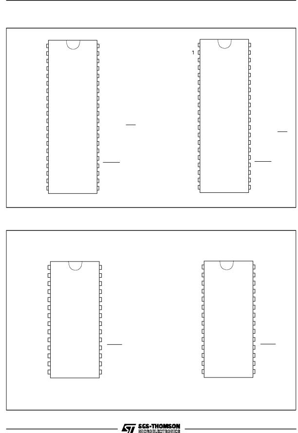
Figure 1. ST63126, 156 Pin Configuration
BSW0 |
1 |
40 |
VDD |
BSW1 |
2 |
39 |
DA3 |
BSW2 |
3 |
38 |
DA2 |
BSW3 |
4 |
37 |
DA1 |
KBY0 |
5 |
36 |
DA0 |
KBY 1 |
6 |
35 |
OUT1 |
KBY2 |
7 |
34 |
IRIN |
OSDOSCout |
8 |
33 |
PC7 (B) |
OSDOSCin |
9 |
32 |
PC6 (G) |
(SEN) PB7 |
10 |
31 |
PC5 (R) |
(SDA) PB6 |
11 |
30 |
PC3 (BLANK) |
(SCL) PB5 |
12 |
29 |
PC2 (ON/OFF) |
(HSYNC) PB3 |
13 |
28 |
PC1 |
(VSYNC) PB2 |
14 |
27 |
PC0 |
AFC |
15 |
26 |
OSCout |
TEST (1) |
16 |
25 |
OSCin |
PA6 |
17 |
24 |
RESET |
PA5 |
18 |
23 |
PA1 |
PA4 |
19 |
22 |
PA2 |
VSS |
20 |
21 |
PA3 |
|
|
ST63126 |
VA00282 |
|
|
|
Note 1. This pin is also the VPP input for EPROM based devices
Figure 2. ST63140, 142 Pin Configuration
BSW0 |
1 |
28 |
VDD |
BSW1 |
2 |
27 |
DA0 |
BSW2 |
3 |
26 |
OUT1 |
KBY0 |
4 |
25 |
VS |
KBY1 |
5 |
24 |
PC6 (G) |
KBY2 |
6 |
23 |
PC4 |
OSDOSCout |
7 |
22 |
PC3 (BLANK) |
OSDOSCin |
8 |
21 |
PC2 |
PB3 (HSYNC) |
9 |
20 |
OSCout |
PB2 (VSYNC) |
10 |
19 |
OSCin |
AFC |
11 |
18 |
RESET |
TEST (1) |
12 |
17 |
PA0 |
PA4 |
13 |
16 |
PA1 |
VSS |
14 |
15 |
PA2 |
|
|
|
VR001389 |
ST63140
Note 1. This pin is also the VPP input for EPROM based devices
2/82
BSW0 |
1 |
40 |
VDD |
BSW |
2 |
39 |
DA3 |
BSW2 |
3 |
38 |
DA2 |
BSW3 |
4 |
37 |
DA1 |
KBY0 |
5 |
36 |
DA0 |
KBY 1 |
6 |
35 |
OUT1 |
KBY2 |
7 |
34 |
IRIN |
OSDOSCout |
8 |
33 |
VS |
OSDOSCin |
9 |
32 |
PC7 (B) |
(SEN) PB7 |
10 |
31 |
PC6 (G) |
(SDA) PB6 |
11 |
30 |
PC5 (R) |
(SCL) PB5 |
12 |
29 |
PC3 (BLANK) |
(HSYNC) PB3 |
13 |
28 |
PC2 (ON/OFF) |
(VSYNC) PB2 |
14 |
27 |
PC1 |
AFC |
15 |
26 |
OSCout |
TEST (1) |
16 |
25 |
OSCin |
PA6 |
17 |
24 |
RESET |
PA5 |
18 |
23 |
PA1 |
PA4 |
19 |
22 |
PA2 |
VSS |
20 |
21 |
PA3 |
|
|
|
VA00288 |
ST63156
BSW0 |
1 |
28 |
VDD |
BSW1 |
2 |
27 |
DA0 |
BSW2 |
3 |
26 |
OUT1 |
KBY0 |
4 |
25 |
IRIN |
KBY1 |
5 |
24 |
PC6 (G) |
KBY2 |
6 |
23 |
PC5 (R) |
OSDOSCout |
7 |
22 |
PC4 |
OSDOSCin |
8 |
21 |
PC2 |
PB3 (HSYNC) |
9 |
20 |
OSCout |
PB2 (VSYNC) |
10 |
19 |
OSCin |
AFC |
11 |
18 |
RESET |
TEST (1) |
12 |
17 |
PA0 |
PA4 |
13 |
16 |
PA1 |
VSS |
14 |
15 |
PA2 |
VR001390
ST63142

GENERAL DESCRIPTION
The ST63140, 142, 126, 156 microcontrollers are members of the 8-bit HCMOS ST631xx family, a series of devices specially oriented to TV applications. Different ROM size and peripheral configurations are available to give the maximum application and cost flexibility. All ST631xx members are based on a building block approach: a common core is surrounded by a combination of on-chip peripherals (macrocells) available from a standard library. These peripherals are designed with the same Core technology providing full compatibility and short design time. Many of these macrocells are specially dedicated to TV applications. The macrocells of the ST631xx family are: two Timer peripherals each including an 8-bit counter with a
ST63140,142,126,156
7-bit software programmable prescaler (Timer), a digital hardware activated watchdog function (DHWD), a 14-bit voltage synthesis tuning peripheral, a Serial Peripheral Interface (SPI), up to four 6-bit PWM D/A converters, an AFC A/D converter with 0.5V resolution, an on-screen display (OSD) with 15 characters per line and 128 characters (in two banks each of 64 characters). In addition the following memory resources are available: program ROM (7K), data RAM (256 bytes), EEPROM (128 bytes).
Refer to pin configuration figures and to ST631xx device summary (Table 1) for the definition of ST631xx family members and a summary of differences among the different types.
3/82

ST63140,142,126,156
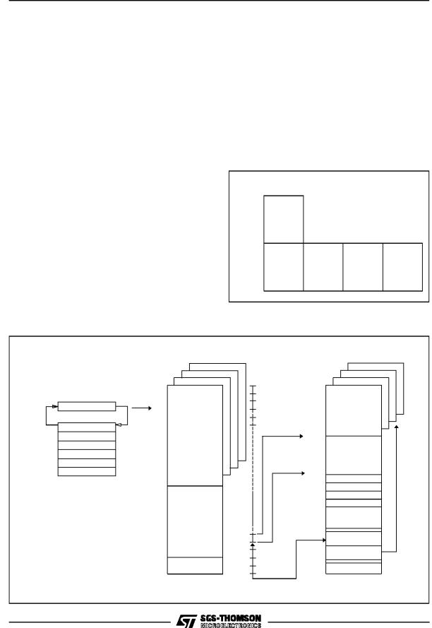
Figure 3. ST631xx Block Diagram
TEST
IRIN/NMI
* Refer To Pin Configuration For Additional Information
TEST
IR INTERRUPT
Input
USER PROGRAM
ROM
8 KBytes
PC
STACK LEVEL 1 STACK LEVEL 2 STACK LEVEL 3 STACK LEVEL 4 STACK LEVEL 5 STACK LEVEL 6
DATA ROM
USER SELECTABLE
DATA RAM
256 Bytes
DATA EEPROM
128 Bytes
8-BIT CORE
POWER SUPPLY |
OSCILLATOR |
RESET |
|
VDD |
VSS |
OSCin OSCout |
RESET |
PORT A |
PA0 - PA7 * |
|
PORT B |
PB2 - PB7 * |
|
PORT C |
PC0 - PC7 * |
|
SERIAL PERIPHERAL |
|
|
INTERFACE |
|
|
TIMER 1 |
|
|
TIMER 2 |
|
|
DIGITAL |
|
|
WATCHDOG/TIMER |
|
|
D / A Outputs |
DA0 - DA3 |
|
VS output & |
AFC & VS * |
|
AFC Input |
||
|
||
ON-SCREEN |
R, G, B, BLANK |
|
DISPLAY |
HSYNC (PB3) |
|
|
VSYNC (PB2) |
|
OSDOSCin OSDOSCout |
VR 01 753E |
|
|
Table 1. Device Summary
DEVICE |
ROM |
RAM |
EEPROM |
I/O |
KBY |
BSW |
AFC |
VS |
D/A |
PACK. |
EMUL. |
|
(Bytes) |
(Bytes) |
(Bytes) |
I/O |
OUT |
DEVICES |
|||||||
|
|
|
|
|
|
|||||||
ST63126 |
8K |
256 |
128 |
12 |
3 |
4 |
YES |
NO |
4 |
PDIP40 |
ST63E126 |
|
ST63156 |
8K |
256 |
128 |
11 |
3 |
4 |
YES |
YES |
4 |
PDIP40 |
ST63E156 |
|
ST63140 |
8K |
256 |
128 |
6 |
3 |
3 |
YES |
YES |
1 |
PDIP28 |
ST6E140 |
|
ST63142 |
8K |
256 |
128 |
6 |
3 |
3 |
YES |
NO |
1 |
PDIP28 |
ST63E142 |
4/82

ST63140,142,126,156
PIN DESCRIPTION
VDD and VSS. Power is supplied to the MCU using these two pins. VDD is power and VSS is the ground connection.
OSCin, OSCout. These pins are internally connected to the on-chip oscillator circuit. A quartz crystal or a ceramic resonator can be connected between these two pins in order to allow the correct operation of the MCU with various stability/cost trade-offs. The OSCin pin is the input pin, the OSCout pin is the output pin.
RESET. The active low RESET pin is used to start the microcontroller to the beginning of its program.
TEST. The TEST pin must be held at VSS for normal operation.
PA0-PA7. These 8 lines are organized as one I/O port (A). Each line may be configured as either an input or as an output under software control of the data direction register. Port A has an open-drain (12V drive) output configuration with direct LED driving capability (30mA, 1V).
PB2-PB3, PB5-PB7. These lines are organized as one I/O port (B). Each line may be configured as either an input with or without internal pull-up resistor or as an output under software control of the data direction register. PB2-PB3 have a push-pull configuration in output mode while PB5-PB7 are open-drain (5V drive).
PB2 and PB3 lines are connected to the VSYNC and HSYNC control signals of the OSD cell; to provide the right signals to the OSD these I/O lines should be programmed in input mode and the user can read ªon the flyº the state of VSYNC and HSYNC signals. PB2 is also connected with the VSYNC Interrupt. The active polarity of VSYNC Interrupt signal is software controlled. The active polarity of these synchronization input pins to the OSD macrocell can be selected by the user as ROM mask option. If the device is specified to have negative logic inputs, then when these signals are low the OSD oscillator stops. If the device is specified to have positive logic inputs, then when these signals are high the OSD oscillator stops.
PB5, PB6 and PB7 lines, when in output modes, are ªANDedº with the SPI control signals. PB5 is connected with the SPI clock signal (SCL), PB6 with the SPI data signal (SDA) while PB7 is connected with SPI enable signal (SEN).
PC0-PC7. These 8 lines are organized as one I/O port (C). Each line may be configured as either an input with or without internal pull-up resistor or as an output under software control of the data direction register. PC0-PC2, PC4 have a push-pull configuration in output mode while PC3, PC5-PC7 (OSD signals) are open-drain (5V drive). PC3, PC5 , PC6 and PC7 lines when in output mode are ªANDedº with the character and blank signals of the OSD cell. PC3 is connected with the OSD BLANK signal, PC5, PC6 and PC7 with the OSD R, G and B signals. The active polarity of these signals can be selected by the user as ROM mask option. PC2 is also used as TV set ON-OFF switch (5V drive).
DA0-DA3. These pins are the four PWM D/A outputs (with 32kHz repetition) of the 6-bit on-chip D/A converters. The PWM function can be disabled by software and these lines can be used as general purpose open-drain outputs (12V drive).
IRIN. This pin is the external NMI of the MCU.
OUT1. This pin is the 62.5kHz output specially suited to drive multi-standard chroma processors. This function can be disabled by software and the pin can be used as general purpose open-drain output (12V drive).
BSW0-BSW3. These output pins can be used to select up to 4 tuning bands. These lines are configured as open-drain outputs (12V drive).
KBY0-KBY2. These pins are input only and can be used for keyboard scan. They have CMOS threshold levels with Schmitt Trigger and on-chip 100kΩ pull-up resistors.
AFC. This is the input of the on-chip 10 level comparator that can be used to implement the AFC function. This pin is an high impedance input able to withstand signals with a peak amplitude up to 12V.
OSDOSCin, OSDOSCout. These are the On Screen Display oscillator terminals. An oscillation capacitor and coil network have to be connected to provide the right signal to the OSD.
VS. This is the output pin of the on-chip 14-bit voltage synthesis tuning cell (VS). The tuning signal present at this pin gives an approximate resolution of 40kHz per step over the UHF band. This line is a push-pull output with standard drive (ST63140, ST63156 only).
5/82

ST63140,142,126,156
Table 2. Pin Summary
Pin Function |
Description |
DA0 to DA3 |
Output, Open-Drain, 12V |
BSW0 to BSW3 |
Output, Open-Drain, 12V |
IRIN |
Input, Resistive Bias, Schmitt Trigger |
AFC |
Input, High Impedance, 12V |
OUT1 |
Output, Open-Drain, 12V |
KBY0 to KBY2 |
Input, Pull-up, Schmitt Trigger |
R,G,B, BLANK |
Output, Open-Drain, 5V |
HSYNC, VSYNC |
Input, Pull-up, Schmitt Trigger |
OSDOSCin |
Input, High Impedance |
OSDOSCout |
Output, Push-Pull |
TEST |
Input, Pull-Down |
OSCin |
Input, Resistive Bias, Schmitt Trigger to Reset Logic Only |
OSCout |
Output, Push-Pull |
RESET |
Input, Pull-up, Schmitt Trigger Input |
VS |
Output, Push-Pull |
PA0-PA6 |
I/O, Open-Drain, 12V, No Input Pull-up, Schmitt Trigger, High Drive |
PB2-PB3, PB5-PB7 |
I/O, Push-Pull, 5V, Input Pull-up, Schmitt Trigger |
PB5-PB7 |
I/O, Open-Drain, 5V, Input Pull-up, Schmitt Trigger |
PC0-PC2, PC4 |
I/O, Push-Pull, 5V, Input Pull-up, Schmitt Trigger |
PC3, PC5-PC7 |
I/O, Open-Drain, 5V, Input Pull-up, Schmitt Trigger |
VDD, VSS |
Power Supply Pins |
6/82
ST63140,142,126,156
ST631xx CORE
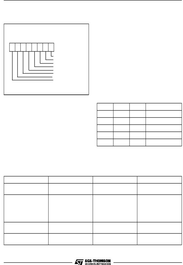
The Core of the ST631xx Family is implemented independently from the I/O or memory configuration. Consequently, it can be treated as an independent central processor communicating with I/O and memory via internal addresses, data, and control busses. The in-core communication is arranged as shown in the following block diagram figure; the controller being externally linked to both the reset and the oscillator, while the core is linked to the dedicated on-chip macrocells peripherals via the serial data bus and indirectly for interrupt purposes through the control registers.
Registers
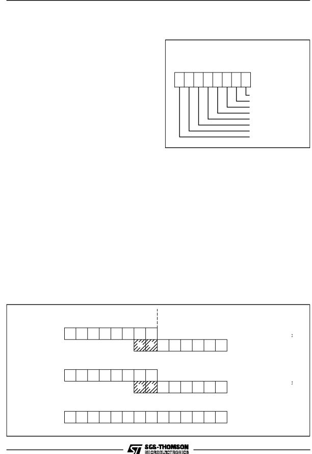
The ST631xx Family Core has six registers and three pairs of flags available to the programmer. They are shown in Figure 5 and are explained in the following paragraphs together with the program and data memory page registers.
Accumulator (A). The accumulator is an 8-bit general purpose register used in all arithmetic calculations, logical operations, and data manipulations. The accumulator is addressed in the data space as RAM location at address FFh .
Accordingly, the ST631xx instruction set can use the accumulator as any other register of the data space.
Figure 4. ST631xx Core Block Diagram
Figure 5. ST631xx Core Programming Model
INDEX |
b7 |
X REG. POINTER |
b0 |
SHORT |
|
|
|
|
|
||
REGISTER |
b7 |
Y REG. POINTER |
b0 |
DIRECT |
|
|
|
|
|
|
ADDRESSING |
|
b7 |
V REGISTER |
b0 |
MODE |
|
|
b7 |
W REGISTER |
|
b0 |
|
|
b7 |
ACCUMULATOR |
b0 |
|
|
b11 |
PROGRAM COUNTER |
|
b0 |
|
|
|
SIX LEVELS |
|
|
|
|
|
STACK REGISTER |
|
|
|
|
NORMAL FLAGS |
|
C |
Z |
|
|
INTERRUPT FLAGS |
C |
Z |
|
||
NMI FLAGS |
|
C |
Z |
|
|
|
|
|
|
|
VA000423 |
|
|
0,0 1 TO 8MHz |
|
|
|
|
RESET |
OS Cin |
OSCout |
|
|
|
|
CONTROLLER |
|
|
INTERRUPTS |
|
|
|
|
|
DATA SPACE |
|
|
FLAG |
CONTROL |
|
|
|
OPCODE |
VALUES |
SIGNALS |
ADDRESS / READ LINE |
|
|
|
2 |
|
|
DATA |
|
|
|
|
|
|
|
|
|
|
|
RAM / EEPROM |
PROGRAM |
|
|
|
|
|
ROM/EPROM |
|
|
|
|
|
|
|
|
|
ADDRESS |
DATA |
|
|
|
|
256 |
|
|
|
|
|
DECODER |
|
|
|
|
|
ROM / EPROM |
|
|
|
A-DATA |
B-DATA |
|
|
|
|
|
|
|
DEDICATIONS |
|
Progr am Counter |
|
|
ACCUMULATOR |
|
12 |
a nd |
FLAGS |
|
|
|
|
6 LAYER STACK |
|
ALU |
|
|
RESULTS TO DATA SPACE ( WRITE LINE )
VR001811
7/82

ST63140,142,126,156
ST631xx CORE (Continued)
Indirect Registers (X, Y). These two indirect registers are used as pointers to the memory locations in the data space. They are used in the register-in- direct addressing mode.These registers can be addressed in the data space as RAM locations at the 80h (X) and 81h (Y) addresses. They can also be accessed with the direct, short direct, or bit direct addressing modes. Accordingly, the ST631xx instruction set can use the indirect registers as any other register of the data space.
Short Direct Registers (V, W). These two registers are used to save one byte in short direct addressing mode. These registers can be addressed in the data space as RAM locations at the 82h (V) and 83H (W) addresses. They can also be accessed with the direct and bit direct addressing modes. Accordingly, the ST631xx instruction set can use the short direct registers as any other register of the data space.
Program Counter (PC)
The program counter is a 12-bit register that contains the address of the next ROM location to be processed by the core. This ROM location may be an opcode, an operand, or an address of operand. The 12-bit length allows the direct addressing of 4096 bytes in the program space. Nevertheless, if the program space contains more than 4096 locations, the further program space can be addressed by using the Program ROM Page Register. The PC value is incremented, after it is read for the address of the current instruction, by sending it through the ALU, so giving the address of the next byte in the program. To execute relative jumps the PC and the offset values are shifted through the ALU, where they will be added, and the result is shifted back into the PC. The program counter can be changed in the following ways:
JP (Jump) instruction.... |
PC = Jump address |
CALL instruction ........... |
PC= Call address |
Relative Branch |
|
instructions ................... |
PC= PC+offset |
Interrupt........................ |
PC= Interrupt vector |
Reset............................ |
PC= Reset vector |
RET & RETI instructions |
............PC=Pop (stack) |
Normal instruction ........ |
PC = PC+1 |
Flags (C, Z)
The ST631xx Core includes three pairs of flags that correspond to 3 different modes: normal mode, interrupt mode and Non-Maskable-Inter- rupt-Mode. Each pair consists of a CARRY flag and a ZERO flag. One pair (CN, ZN) is used during normal operation, one pair is used during the interrupt mode (CI,ZI) and one is used during the notmaskable interrupt mode (CNMI, ZNMI).
The ST631xx Core uses the pair of flags that corresponds to the actual mode: as soon as an interrupt (resp. a Non-Maskable-Interrupt) is generated, the ST631xx Core uses the interrupt flags (resp. the NMI flags) instead of the normal flags. When the RETI instruction is executed, the normal flags (resp. the interrupt flags) are restored if the MCU was in the normal mode (resp. in the interrupt mode) before the interrupt. Should be observed that each flag set can only be addressed in its own routine (Not-maskable interrupt, normal interrupt or main routine). The interrupt flags are not cleared during the context switching and so, they remain in the state they were at the exit of the last routine switching.
The Carry flag is set when a carry or a borrow occurs during arithmetic operations, otherwise it is cleared. The Carry flag is also set to the value of the bit tested in a bit test instruction, and participates in the rotate left instruction.
The Zero flag is set if the result of the last arithmetic or logical operation was equal to zero, otherwise it is cleared.
The switching between these three sets is automatically performed when an NMI, an interrupt and a RETI instructions occur. As the NMI mode is automatically selected after the reset of the MCU, the ST631xx Core uses at first the NMI flags.
8/82

ST631xxx CORE (Continued)
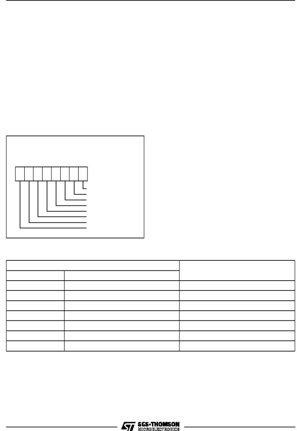
Stack
The ST631xx Core includes true LIFO hardware stack that eliminates the need for a stack pointer. The stack consists of six separate 12-bit RAM locations that do not belong to the data space RAM area. When a subroutine call (or interrupt request) occurs, the contents of each level is shifted into the next level while the content of the PC is shifted into the first level (the value of the sixth level will be lost). When subroutine or interrupt return occurs (RET or RETI instructions), the first level register is shifted back into the PC and the value of each level is shifted back into the previous level. These two operating modes are described in Figure 6. Since the accumulator, as all other data space registers, is not stored in this stack the handling of this registers shall be performed inside the subroutine. The stack pointer will remain in its deepest position, if more than 6 calls or interrupts are executed, so that the last return address will be lost. It will also remain in its highest position if the stack is empty and a RET or RETI is executed. In this case the next instruction will be executed.
ST63140,142,126,156
Figure 6. Stack Operation
RET OR RETI
WHEN
OCCURS
PROGRAM COUNTER
STACK LEVEL 1
STACK LEVEL 1
STACK LEVEL 1
STACK LEVEL 1
STACK LEVEL 1
STACK LEVEL 1
WHEN CALL
OR
INTERRUPT REQUEST
OCCURS
VA000424
9/82
ST63140,142,126,156
MEMORY SPACES
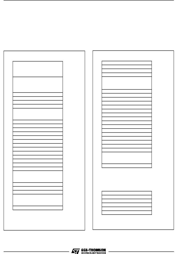
The MCUs operate in three different memory spaces: Program Space, Data Space, and Stack Space. A description of these spaces is shown in the following Figures.
Program Space
The program space is physically implemented in the ROM and includes all the instructions that are to be executed, as well as the data required for the immediate addressing mode instructions, the reserved test area and user vectors. It is addressed thanks to the 12-bit Program Counter register (PC register) and so, the ST631xx Core can directly address up to 4K bytes of Program Space. Nevertheless, the Program Space can be extended by the addition of 2-Kbyte ROM banks as it is shown in Figure 8 in which the 8K bytes memory is described.
These banks are addressed by pointing to the 000h-7FFh locations of the Program Space thanks to the Program Counter, and by writing the appropriate code in the Program ROM Page Register (PRPR) located at address CAh of the Data Space. Because interrupts and common subroutines should be available all the time only the lower 2K bytes of the 4K program space are bank switched while the upper 2K bytes can be seen as
static space. Table 3 gives the codes that allow the selection of the correspondingbanks.
Note that, from the memory point of view, the Page 1 and the Static Page represent the same physical memory: it is only a different way of addressing the same location. On the ST631xx a total of 8192 bytes of ROM have been implemented; 7948 are available as user ROM while 244 are reserved for testing.
Figure 8. ST631xx 8K Bytes Program Space
Addressing Description
Program |
|
|
|
|
counter |
0000h |
|
1FFFh |
|
space |
|
|
|
|
0FFFh |
|
|
|
|
|
Static Page |
|
|
|
|
Page 1 |
|
|
|
0800h |
|
|
|
|
07FFh |
|
|
|
|
|
Page 0 |
Page 1 |
Page 2 |
Page 3 |
|
Static Page |
|||
|
|
|
|
|
0000h |
|
|
|
|
Figure 7. ST631xx Memory Addressing Description Diagram
STACK SPAC E |
PROGRAM SPACE |
DATA SPACE |
|
0000h |
000h |
PROGRAM COUNTER |
|
RAM / EEPROM |
|
|
|
|
|
BANKING AR EA |
|
|
|
0-63 |
STACK LEVEL 1 |
|
|
03Fh |
STACK LEVEL 2 |
|
ROM |
|
|
040h |
||
STACK LEVEL 3 |
|
|
|
|
|
|
|
STACK LEVEL 4 |
|
|
|
STACK LEVEL 5 |
|
|
070h |
STACK LEVEL 6 |
|
|
|
|
|
080h |
|
|
07FFh |
|
|
|
|
081h |
|
|
0800h |
|
|
|
|
082h |
|
|
|
|
|
|
|
|
083h |
|
|
|
084h |
|
|
ROM |
0C0h |
|
0FF0h |
|
|
|
|
INTERRUPT & |
|
|
0FFFh |
RESET VEC TOR S |
0FFh |
|
|
|
DATA ROM
WINDOW
XREGISTER
YREGISTER
VREGISTER W REGISTER
RA M
DATA ROM
WIND OW SELECT
DATA RAM
BANK S ELECT
AC CUMUL ATOR
VR001568
10/82
ST63140,142,126,156
MEMORY SPACES (Continued)
Figure 11. Program ROM Page Register
PRPR
Program ROM Page Register
(CAh, Write Only)
D7 D6 D5 D4 D3 D2 D1 D0
PRPR0 = PROG.ROM Select 0
PRPR1 = PROG.ROM Select 1
UNUSED
UNUSED
UNUSED
UNUSED
UNUSED
UNUSED
Care is required when handling the PRPR as it is write only. For this reason, it is not allowed to change the PRPR contents while executing interrupts drivers, as the driver cannot save and than restore its previous content. Anyway, this operation may be necessary if the sum of common routines and interrupt drivers will take more than 2K bytes; in this case could be necessary to divide the interrupt driver in a (minor) part in the static page (start and end), and in the second (major) part in one dynamic page. If it is impossible to avoid the writing of this register in interrupts drivers, an image of this register must be saved in a RAM location, and each time the program writes the PRPR it writes also the image register. The image register must be written first, so if an interrupt occurs between the two instructions the PRPR is not affected.
D7-D2. These bits are not used.
PRPR1-PRPR0. These are the program ROM banking bits and the value loaded selects the corresponding page to be addressed in the lower part of 4K program address space as specified in Table 3. This register is undefinedon reset.
Note:
Only the lower part of address space has been bankswitched because interrupt vectors and common subroutines should be available all the time. The reason of this structure is due to the fact that it is not possible to jump from a dynamic page to another, unless jumping back to the static page, changing contents of PRPR, and, then, jumping to a different dynamic page.
Table 4. ST631xx Program ROM Map
Table 3. Program ROM Page Register Coding
PRPR1 |
PRPR0 |
PC11 |
Memory Page |
X |
X |
1 |
Static Page (Page1) |
0 |
0 |
0 |
Page 0 |
0 |
1 |
0 |
Page 1 (Static Page) |
1 |
0 |
0 |
Page 2 |
1 |
1 |
0 |
Page 3 |
This register is undefined on reset. Neither read nor single bit instructions may be used to address this register.
ROM Page |
Device Address |
Device Address (1) |
Description |
|
PAGE 0 |
0000h-007Fh |
0000h-007Fh |
Reserved |
|
0080h-07FFh |
0080h-07FFh |
User ROM |
||
|
||||
|
0800h-0F9Fh |
0800h-0F9Fh |
User ROM |
|
|
0FA0h-0FEFh |
0FA0h-0FEFh |
Reserved |
|
PAGE 1 |
0FF0h-0FF7h |
0FF0h-0FF7h |
Interrupt Vectors |
|
ªSTATICº |
0FF8h-0FFBh |
0FF8h-0FFBh |
Reserved |
|
|
0FFCh-0FFDh |
0FFCh-0FFDh |
NMI Vector |
|
|
0FFEh-0FFFh |
0FFEh-0FFFh |
Reset Vector |
|
PAGE 2 |
0000h-000Fh |
1000h-100Fh |
Reserved |
|
0010h-07FFh |
1010h-17FFh |
User ROM |
||
|
||||
PAGE 3 |
0000h-000Fh |
1800h-180Fh |
Reserved |
|
0010h-07FFh |
1810h-1FFFh |
User ROM |
||
|
Note 1. EPROM addresses relate to the use of ST63E1xx EPROM Emulation device.
11/82
ST63140,142,126,156
MEMORY SPACES (Continued)
Data Space
The instruction set of the ST631xx Core operates on a specific space, named Data Space that contains all the data necessary for the processing of the program. The Data Space allows the address-
Figure 12. ST631xx Data Space
b7 |
b0 |
|
|
|
000h |
|
DATA RAM/EEPROM/OSD |
|
|
BANK AREA |
|
|
|
03Fh |
|
|
040h |
|
DATA ROM |
|
|
WINDOW AREA |
|
|
|
07Fh |
|
X REGISTER |
080h |
|
Y REGISTER |
081h |
|
V REGISTER |
082h |
|
W REGISTER |
083h |
|
|
084h |
|
DATA RAM |
|
|
|
0BFh |
|
PORT A DATA REGISTER |
0C0h |
|
PORT B DATA REGISTER |
0C1h |
|
PORT C DATA REGISTER |
0C2h |
|
RESERVED |
0C3h |
PORT A DIRECTION REGISTER |
0C4h |
|
PORT B DIRECTION REGISTER |
0C5h |
|
PORT C DIRECTION REGISTER |
0C6h |
|
|
RESERVED |
0C7h |
INTERR UPT OPTION REGISTER |
0C8h |
|
DATA ROM WINDOW REGISTER |
0C9h |
|
PROGRAM ROM PAGE REGISTER |
0CAh |
|
|
RESERVED |
0CBh |
|
SPI DATA REGISTER |
0CCh |
|
|
0CDh |
|
RESERVED |
|
|
|
0D1h |
TIMER 1 PRESCALER REGISTER |
0D2h |
|
TIMER 1 COUNTER REGISTER |
0D3h |
|
TIMER 1 STATUS/CONTROL REG. |
0D4h |
|
|
|
0D5h |
|
RESERVED |
|
|
|
0D7h |
|
WATCHD OG REGISTER |
0D8h |
ing of RAM (256 bytes for the ST631xx family), EEPROM (128 bytes), ST631xx Core/peripheral registers, and read-only data such as constants and the look-up tables.
Figure 13. ST631xx Data Space (Continued)
b7 |
b0 |
|
|
RESERVED |
0D9h |
TIMER 2 PRESCALER REGISTER |
0DAh |
|
TIMER 2 COUNTER REGISTER |
0DBh |
|
TIMER 2 STATUS CONTROL REG. |
0DCh |
|
|
|
0DDh |
|
RESERVED |
|
|
|
0DFh |
DA0 DATA/CONTROL REGISTER |
0E0h |
|
DA1 DATA/CONTROL REGISTER |
0E1h |
|
DA2 DATA/CONTROL REGISTER |
0E2h |
|
DA3 DATA/CONTROL REGISTER |
0E3h |
|
|
AFC RESULT REGISTER |
0E4h |
|
KEYBOARD INPUT REGISTER |
0E5h |
|
RESERVED |
0E6h |
|
RESERVED |
0E7h |
|
DATA RAM BANK REGISTER |
0E8h |
|
BSW CONTROL REGISTER |
0E9h |
EEPROM CONTROL REGISTER |
0EAh |
|
|
SPI CONTROL REGISTER 1 |
0EBh |
|
SPI CONTROL REGISTER 2 |
0ECh |
|
VS DATA REGISTER 1 |
0EDh |
|
VS DATA REGISTER 2 |
0EEh |
OSD CHARAC. BANK SELECT REG. 0EFh |
||
|
|
0F0h |
|
RESERVED |
|
|
|
0FEh |
|
ACCUMULATOR |
0FFh |
OSD CONTROL REGISTERS LOCATED |
|
|
IN PAGE6 OF BANKED DATA RAM |
|
|
VERTICAL START ADDRESS REG. |
010h |
|
HORIZONTALSTART ADDRESS REG. 011h |
||
|
VERTICAL SPACE REGISTER |
012h |
HORIZONTAL SPACE REGISTER |
013h |
|
BACKGROUND COLOUR REGISTER |
014h |
|
|
GLOBAL ENABLE REGISTER |
017h |
12/82
ST63140,142,126,156
MEMORY SPACES (Continued)
Data ROM Addressing. All the read-only data are physically implemented in the ROM in which the Program Space is also implemented. The ROM therefore contains the program to be executed and also the constants and the look-up tables needed for the program. The locations of Data Space in which the different constants and look-up tables are addressed by the ST631xx Core can be considered as being a 64-byte window through which it is possible to access to the read-only data stored in the ROM. This window is located from address 40H to address 7Fh in the Data space and allows the direct reading of the bytes from the address 000h to address 03Fh in the ROM. All the bytes of the ROM can be used to store either instructions or read-only data. Indeed, the window can be moved by step of 64 bytes along the ROM in writing the appropriate code in the Write-only Data ROM Window register (DRWR, location C9h). The effective address of the byte to be read as a data in the ROM is obtained by the concatenation of the 6 less significant bits of the address in the Data Space (as less significant bits) and the content of the DRWR (as most significant bits). So when addressing location 40h of data space, and 0 is loaded in the DRWR, the physical addressed location in ROM is 00h.
Figure 15. Data ROM Window Memory Addressing
Figure 14. Data ROM Window Register
DWR
Data ROM Window Register
(C9h, Write Only)
D7 D6 D5 D4 D3 D2 D1 D0
DWR0 = Data ROMWindow 0
DWR1 = Data ROMWindow 1
DWR2 = Data ROMWindow 2
DWR3 = Data ROMWindow 3
DWR4 = Data ROMWindow 4
DWR5 = Data ROMWindow 5
DWR6 = Data ROMWindow 6
UNUSED
D7. This bit is not used.
DWR6-DWR0. These are the Data Rom Window bits thatcorrespondto theupperbitsof data ROMprogram space. This register is undefined after reset.
This register is undefined on reset. Neither read nor single bit instructions may be used to address this register.
Note. Care is required when handling the DRWR as it is write only. For this reason, it is not allowed to change the DRWR contents while executing interrupts drivers, as the driver cannot save and than restore its previous content. If it is impossible to avoid the writing of this register in interrupts drivers, an image of this register must be saved in a RAM location, and each time the program writes the DRWR it writes also the image register. The image register must be written first, so if an interrupt occurs between the two instructions the DRWR register is not affected.
DATA ROM |
13 12 |
11 |
10 9 |
8 |
7 |
6 5 |
4 |
3 |
2 |
1 |
0 |
PROGRAM SPACE ADDRESS |
|
|
|
|
|
|
|
|
|
|
|
READ |
|
WINDOW REGISTER 7 6 |
5 |
4 3 |
2 |
1 |
0 |
|
|
|
|
|
||
|
|
|
|
|
|
|||||||
CONTENTS |
|
|
|
|
|
5 |
4 |
3 |
2 |
1 |
0 |
DATA SPACE ADDRESS |
(DWR) |
|
|
|
|
|
|||||||
|
|
|
|
0 |
1 |
|
|
|
|
|
40h-7Fh |
|
|
|
|
|
|
|
|
|
|
|
|||
|
|
|
|
|
|
|
|
|
|
|
|
IN INSTRUCTION |
Example:
DWR=28h |
0 |
0 |
1 |
0 |
1 |
0 |
0 |
0 |
|
|
|
|
|
|
|
|
|
|
|
|
|
|
0 |
1 |
0 |
1 |
1 |
0 |
0 |
1 |
DATA SPACE ADDRESS |
|
|
|
|
|
|
|
59h |
||||||||
|
|
|
|
|
|
|
|
|
|
|
|
|
|
|
|
ROM |
0 |
0 |
1 |
0 |
1 |
0 |
0 |
0 |
0 |
1 |
1 |
0 |
0 |
1 |
|
ADDRESS:A19h |
|
||||||||||||||
|
|
|
|
|
|
|
|
|
|
|
|
|
|
|
VR01573B
13/82
ST63140,142,126,156
MEMORY SPACES (Continued)
Data RAM/EEPROM/OSD RAM Addressing
In all members of the ST631xx family 64 bytes of data RAM are directly addressable in the data space from 80h to BFh addresses. The additional 192 bytesof RAM, the 128 bytes of EEPROM , and the OSD RAM can be addressed using the banks of 64 bytes located between addresses 00h and 3Fh. The selection of the bank is done by programming the Data RAM Bank Register (DRBR) located at the E8h address of the Data Space. In this way each bank of RAM, EEPROM or OSD RAM can select 64 bytes at a time. No more than one bank should be set at a time.
Figure 16. Data RAM Bank Register
DRBR
Data RAM
Bank Register
(E8h, Write Only)
D7 |
D6 |
D5 |
D4 |
D3 |
D2 |
D1 |
D0 |
DRBR0 = Data RAM Bank0
DRBR1= Data RAM Bank 0
DRBR2= Data RAM Bank 0
DRBR3= Data RAM Bank 0
DRBR4= Data RAM Bank 0
DRBR5= Data RAM Bank 0
DRBR6= Data RAM Bank 0
UNUSED
Table 5. Data RAM Bank Register Set-up
|
DRBR Value |
Hex. |
Binary |
01h |
0000 0001 |
02h |
0000 0010 |
04h |
0000 0100 |
08h |
000 1000 |
10h |
0001 0000 |
20h |
0010 0000 |
40h |
0100 0000 |
14/82
D7. This bit is not used.
DRBR6, DRBR5. Each of these bits, when set, will select one OSD RAM register page.
DRBR4,DRBR3,DRBR2. Each of these bits, when set, will select one RAM page.
DRBR1,DRBR0. These bits select the EEPROM pages.
This register is undefined after reset. Neither read nor single bit instructions may be used to address this register.
Table 5 summarizes how to set the Data RAM Bank Register in order to select the various banks or pages.
Note :
Care is required when handling the DRBR as it is write only. For this reason, it is not allowed to change the DRBR contents while executing interrupts drivers, as the driver cannot save and than restore its previous content. If it is impossible to avoid the writing of this register in interrupts drivers, an image of this register must be saved in a RAM location, and each time the program writes the DRBR it writes also the image register.
The image register must be written first, so if an interrupt occurs between the two instructions the DRBR is not affected.
Selection
EEPROM Page 0
EEPROM Page 1
RAM Page 2
RAM Page 3
RAM Page 4
OSD Page 5
OSD Page 6

ST63140,142,126,156
MEMORY SPACES (Continued)
EEPROM Description
The data space of ST631xx family from 00h to 3Fh is paged as described in Table 5. 128 bytes of EEPROM located in 2 pages of 64 bytes (pages 0, and 1, see Table 5).
Through the programming of the Data RAM Bank Register (DRBR=E8h) the user can select the bank or page leaving unaffected the way to address the static registers. The way to address the ªdynamicº page is to set the DRBR as described in Table 5 (e.g. to select EEPROM page 0, the DRBR has to be loaded with content 01h, see Data RAM/EEPROM/OSD RAM addressing for additional information). Bits 0 and 1 of the DRBR are dedicated to the EEPROM.
The EEPROM pages do not require dedicated instructions to be accessed in reading or writing. The EEPROM is controlled by the EEPROM Control Register (EECR=EAh). Any EEPROM location can be read just like any other data location, also in terms of access time.
To write an EEPROM location takes an average time of 5 ms (10ms max) and during this time the EEPROM is not accessible by the Core. A busy flag can be read by the Core to know the EEPROM status before trying any access. In writing the EEPROM can work in two modes: Byte Mode (BMODE) and Parallel Mode (PMODE). The BMODE is the normal way to use the EEPROM and consists in accessing one byte at a time. The PMODE consists in accessing 8 bytes per time.
Figure 17. EEPROM Control Register
EECR
EEPROM Control Register
(EAh, Read/Write)
D7 D6 D5 D4 D3 D2 D1 D0
EN = EEPROM Enable Bit
BS = EEPROM Busy Bit
PE = Parallel Mode Enable Bit
PS = Parallel Start Bit
Reserved (Must be set Low)
Reserved (Must be set Low)
SB = Stand-by Enable Bit
Unused
D7. Not used
SB. WRITE ONLY. If this bit is set the EEPROM is disabled (any access will be meaningless) and the power consumption of the EEPROM is reduced to the leakage values.
D5, D4. Reserved, they must be set to zero.
PS. SET ONLY. Once in Parallel Mode, as soon as the user software sets the PS bit the parallel writing of the 8 adjacent registers will start. PS is internally reset at the end of the programming procedure. Note that less than 8 bytes can be written; after parallel programming the remaining undefined bytes will have no particular content.
PE. WRITE ONLY. This bit must be set by the user program in order to perform parallel programming (more bytes per time). If PE is set and the ªparallel start bitº (PS) is low, up to 8 adjacent bytes can be written at the maximum speed, the content being stored in volatile registers. These 8 adjacent bytes can be considered as row, whose A7, A6, A5, A4, A3 are fixed while A2, A1 and A0 are thechanging bytes. PE is automatically reset at the end of any parallel programming procedure. PE can be reset by the user software before starting the programming procedure, leaving unchanged the EEPROM registers.
BS. READ ONLY. This bit will be automatically set by the CORE when the user program modifies an EEPROM register. The user program has to test it before any read or write EEPROM operation; any attempt to access the EEPROM while ªbusy bitº is set will be aborted and the writing procedure in progress completed.
EN. WRITE ONLY. This bit MUST be set to one in order to write any EEPROM register. If the user program will attempt to write the EEPROM when EN= ª0º the involved registers will be unaffected and the ªbusy bitº will not be set.
AfterRESET the contentof EECR register will be 00h.
Notes :
When the EEPROM is busy (BS=ª1º) the EECR can not be accessed in write mode, it is only possible to read BS status. This implies that as long as the EEPROM is busy it is not possible to change the status of the EEPROM control register. EECR bits 4 and 5 are reserved for test purposes, and must never be set to ª1º.
15/82

ST63140,142,126,156
MEMORY SPACES (Continued)
Additional Notes on Parallel Mode. If the user wants to perform a parallel programming the first action should be the set to one the PE bit; from this moment the first time the EEPROM will be addressed in writing, the ROW address will be latched and it will be possible to change it only at the end of the programming procedure or by resetting PE without programming the EEPROM. After the ROW address latching the Core can ªseeº just one EEPROM row (the selected one) and any attempt to write or read other rows will produce errors. Do not read the EEPROM while PE is set.
As soon as PE bit is set, the 8 volatile ROW latches are cleared. From this moment the user can load data in the whole ROW or just in a subset. PS setting will modify the EEPROM registers corresponding to the ROW latches accessed after PE. For example, if the software sets PE and accesses EEPROM in writing at addresses 18h,1Ah,1Bh and then sets PS, these three registers will be modified at the same time; the remaining bytes will have no particular content. Note that PE is internally reset at the end of the programming procedure. This implies that the user must set PE bit between two parallel programming procedures. Anyway the user can set and then reset PE without performing any EEPROM programming. PS is a set only bit and is internally reset at the end of the programming procedure. Note that if the user tries to set PS while PE is not set there will not be any programming procedure and the PS bit will be unaffected. Consequently PS bit can not be set if EN is low. PS can be affected by the user set if, and only if, EN and PE bits are also set to one.
STACK SPACE
The stack space consists of six 12 bit registers that are used for stacking subroutine and interrupt return addresses plus the current program counter register.
INTERRUPT
The ST631xx Core can manage 4 different maskable interrupt sources, plus one non-maskable interrupt source (top priority level interrupt). Each source is associated with a particular interrupt vector that contains a Jump instruction to the related interrupt service routine. Each vector is located in the Program Space at a particular address (see Table 6). When a source provides an interrupt request, and the request processing is also enabled by the ST631xx Core, then the PC register is loaded with the address of the interrupt vector (i.e. of the Jump instruction). Finally, the PC is loaded with the address of the Jump instruction and the interrupt routine is processed.
The relationship between vector and source and the associated priority is hardware fixed for the different ST631xx devices. For some interrupt sources it is also possible to select by software the kind of event that will generate the interrupt.
All interrupts can be disabled by writing to the GEN bit (global interrupt enable) of the interrupt option register (address C8h). After a reset, ST631xx is in non maskable interrupt mode, so no interrupts will be accepted and NMI flags will be used, until a RETI instruction is executed. If an interrupt is executed, one special cycle is made by the core, during that the PC is set to the related interrupt vector address. A jump instruction at this address has to redirect program execution to the beginning of the related interrupt routine. The interrupt detecting cycle, also resets the related interrupt flag (not available to the user), so that another interrupt can be stored for this current vector, while its driver is under execution.
If additional interrupts arrive from the same source, they will be lost. NMI can interrupt other interrupt routines at any time, while other interrupts cannot interrupt each other. If more than one interrupt is waiting for service, they are executed according to their priority. The lower the number, the higher the priority. Priority is, therefore, fixed. Interrupts are checked during the last cycle of an instruction (RETI included). Level sensitive interrupts have to be valid during this period.
16/82
INTERRUPT (Continued)
Table 6. Interrupt Vectors/SourcesRelationships
Interrupt |
Associated |
Vector Address |
|
Source |
Vector |
||
|
|||
IRIN/NMI |
Interrupt |
0FFCh-0FFDh |
|
Pin (1) |
Vector # 0 (NMI) |
||
None (2) |
Interrupt |
0FF6h-0FF7h |
|
|
Vector # 1 |
|
|
Vsync |
Interrupt |
0FF4h-0FF5h |
|
Vector # 2 |
|||
|
|
||
Timer 1 |
Interrupt |
0FF2h-0FF3h |
|
Vector # 3 |
|||
|
|
||
Timer 2 |
Interrupt |
0FF0h-0FF1h |
|
Vector # 4 |
|||
|
|
Notes:
1.This pin is associated with the NMI Interrupt Vector
2.This vector is not used in ST631xx.
Interrupt Vectors/Sources
The ST631xx Core includes 5 different interrupt vectors in order to branch to 5 different interrupt routines. The interrupt vectors are located in the fixed (or static) page of the Program Space.
The interrupt vector associated with the non-mask- able interrupt source is named interrupt vector #0. It is located at addresses FFCh,FFDh in the Program Space. This vector is associated with the PC6/IRIN pin.
The interrupt vectors located at addresses (FF6h,FF7h), (FF4h,FF5h), (FF2h,FF3h), (FF0h,FF1h) are named interrupt vectors #1, #2, #3 and #4 respectively. These vectors are associated with TIMER 2 (#4), VSYNC (#2), and TIMER 1 (#3). Interrupt vector (#1) is not used on ST631xx.
Interrupt Priority
The non-maskable interrupt request has the highest priority and can interrupt any other interrupt routines at any time, nevertheless the other interrupts cannot interrupt each other. If more than one interrupt request is pending, they are processed by the ST631xx Core according to their priority level: vector #1 has the higher priority while vector #4 the lower. The priority of each interrupt source is hardware fixed.
ST63140,142,126,156
Interrupt Option Register
The Interrupt Option Register (IOR register, location C8h) is used to enable/disable the individual interrupt sources and to select the operating mode of the external interrupt inputs. This register can be addressed in the Data Space as RAM location at the C8h address, nevertheless it is write-only register that can not be accessed with single-bit operations. The operating modes of the external interrupt inputs associated to interrupt vectors #1 and #2 are selected through bits 5 and 6 of the IOR register.
Figure 18. Interrupt Option Register
IOR
Interr upt Option Register (C8h, Write Only)
D7 |
D6 |
D5 |
D4 |
D3 |
D2 |
D1 |
D0 |
Unuse d
GEN = Global Enable Bit
ES2 = Edge Selection Bit
EL1 = Edge Level Selection Bit
Unuse d
D7. Not used.
EL1. This is the Edge/Level selection bit of interrupt #1. When set to one, the interrupt is generated on low level of the related signal; when cleared to zero, the interrupt is generated on falling edge. The bit is cleared to zero after reset and as no interrupt source is associated to vector #1 on ST631xx, the user must keep this bit at zero to avoid ghost interrupts from this source.
ES2. This is the edge selection bit on interrupt #2. This bit is used on the ST631xx devices with onchip OSD generator for VSYNC detection.
GEN. This is the global enable bit. When set to one all interrupts are globally enabled; when this bit is cleared to zero all interrupts are disabled (EXcluding NMI).
D3 - D0. These bits are not used.
17/82

ST63140,142,126,156
INTERRUPT (Continued)
Interrupt Procedure. The interrupt procedure is very similar to a call procedure, indeed the user can consider the interrupt as an asynchronouscall procedure. As this is an asynchronous event the user does not know about the context and the time at which it occurred. As a result the user should save all the data space registers which will be used inside the interrupt routines. There are separate sets of processor flags for normal, interrupt and non-maskable interrupt modes which are automatically switched and so these do not need to be saved.
The following list summarizes the interrupt procedure:
ST631xx actions
-Interrupt detection
-The flags C and Z of the main routine are exchanged with the flags C and Z of the interrupt routine (or the NMI flags)
-The value of the PC is stored in the first level of the stack
-The normal interrupt lines are inhibited (NMI still active)
-First internal latch is cleared
-The related interrupt vector is loaded in the PC.
User actions
-User selected registers are saved inside the interrupt service routine (normally on a software stack)
-The source of the interrupt is found by polling (if more than one source is associated to the same vector) the interrupt flag of the source.
-Interrupt servicing
-Return from interrupt (RETI)
ST631xx actions
-Automatically the ST631xx core switches back to the normal flags (or the interrupt flags) and pops the previous PC value from the stack
The interrupt routine begins usually by the identification of the device that has generated the interrupt request (by polling). The user should save the registers which are used inside the interrupt routine (that holds relevant data) into a software stack. After the RETI instruction execution, the core carries out the previous actions and the main routine can continue.
18/82
Figure 19. Interrupt Processing Flow-Chart
INSTRUCTION
FE TCH
INST RUCTION
EX ECUTE
INST RUCTION
|
WA S |
NO |
LOAD PC FROM |
|
THE INST RUCTION |
||||
INTERRUPT VECTOR |
||||
|
A RETI |
|
||
|
|
( FFC / FFD ) |
||
|
|
|
||
|
YE S |
|
|
|
YES |
IS THE CORE |
SET |
||
? |
ALREADY IN |
|||
|
INTE RRUPT MASK |
|||
|
NORMAL MODE ? |
|||
|
|
|||
|
NO |
|
|
|
|
CLEAR |
|
PUSH THE |
|
INTERRUPT MASK |
|
PC INTO THE STAC K |
||
|
SELECT |
|
SELECT |
|
PROGRAM FLA GS |
|
INTERNAL MODE FLAG |
||
º POP º
THE STACK ED PC
CHECK IF THERE IS
NO ? AN INTERRUPT REQUES T
AND INTE RRUPT MASK
YES
VA000014
ST631xx Interrupt Details
IR Interrupt (#0). The IRIN Interrupt is connected to the first interrupt #0 (NMI, 0FFCh). If enabled, then an interrupt will be generated on a rising edge at the pin.
Interrupt (#1). On ST631xx no sources are associated to vector (#1). To avoid any ghost interrupt due to interrupt (#1) the user must keep the EL1 bit of IOR register to zero.

INTERRUPT (Continued)
VSYNC Interrupt (#2). The VSYNC Interrupt is connected to the interrupt #2. When disabled the VSYNC INT signal is low. Bit 5 of the interrupt option register C8h is used to select the negative edge (ES2=0) or the positive edge (ES2=1); the edge willdepend on the application. Note that once an edge has been latched, then the only way to remove the latched signal is to service the interrupt. Care must be taken not to generate spurious interrupts. This interrupt may be used for synchronize to the VSYNC signal in order to change characters in the OSD only when the screen is on vertical blanking (if desired). This method may also be used to blink characters.
TIMER 1 Interrupt (#3). The TIMER 1 Interrupt is connected to the fourth interrupt #3 (0FF2h) which detects a low level (latched in the timer).
TIMER 2 Interrupt (#4). The TIMER 2 Interrupt is connected to the fifth interrupt #4 (0FF0h) which detects a high to low level (latched in the timer).
ST63140,142,126,156
Notes: Global disable does not reset edge sensitive interrupt flags. These edge sensitive interrupts become pending again when global disabling is released. Moreover, edge sensitive interrupts are stored in the related flags also when interrupts are globally disabled, unless each edge sensitive interrupt is also individually disabled before the interrupting event happens. Global disable is done by clearing the GEN bit of Interrupt option register, while any individual disable is done in the control register of the peripheral. The on-chip Timer peripherals have an interrupt request flag bit (TMZ), this bit is set to one when the device wants to generate an interrupt request and a mask bit (ETI) that must be set to one to allow the transfer of the flag bit to the Core.
19/82
ST63140,142,126,156
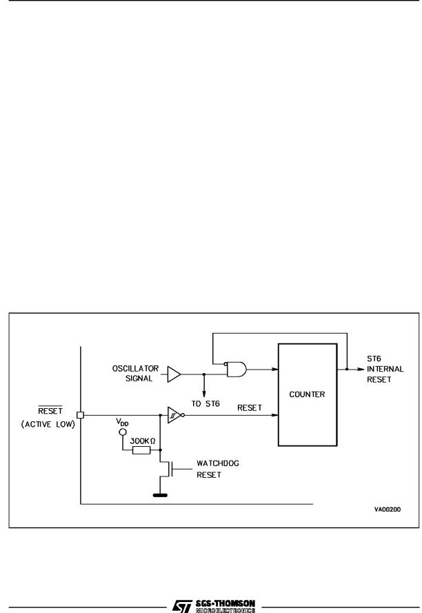
RESET
The ST631xx device can be reset in two ways: by the external reset input (RESET ) tied low, by power-on reset and by the digital Watchdog peripheral.
RESET Input
The external active low RESET pin is used to reset the ST631xx devices and provide an orderly software startup procedure. The activation of the RESET pin may occur in the RUN or WAIT mode. Even short pulses at the reset pin will be accepted since the reset signal is latched internally and is only cleared after 2048 clocks at the oscillator pin. The clocks from the oscillator pin to the reset circuitry are buffered by a Schmitt Trigger so that an oscillator in start-up conditions will not give spurious clocks. The MCU is configured in the Reset mode as long as the signal of the RESET pin is low. The processing of the program is stopped and the standard Input/Outputports (port A, port B and port C) are in the input state (except PC2). As soon as the level on the RESET pin becomes high, the initialization sequence is executed.
Figure 20. Internal Reset Circuit
Watchdog Reset
The ST631xx devices are provided with an onchip hardware activated digital watchdog function in order to provide a graceful recovery from a software upset. If the watchdog register is not refreshed and the end-of-count is reached, then the reset state will be latched into the MCU and an internal circuit pulls down the RESET pin. This also resets the watchdog which subsequently turns off the pull-down and activates the pull-up device at the RESET pin. This causes the positive transition at the RESET pin. The MCU will then exit the reset state after 2048 clocks on the oscillator pin.
Application Notes
An external resistor between VDD and reset pin is not required because an internal pull-up device is provided. The user may prefer to add an external pull-up resistor.
An internal Power-on device does not guarantee that the MCU will exit the reset state when VDD is above 4.5V and therefore the RESET pin should be externally controlled.
20/82
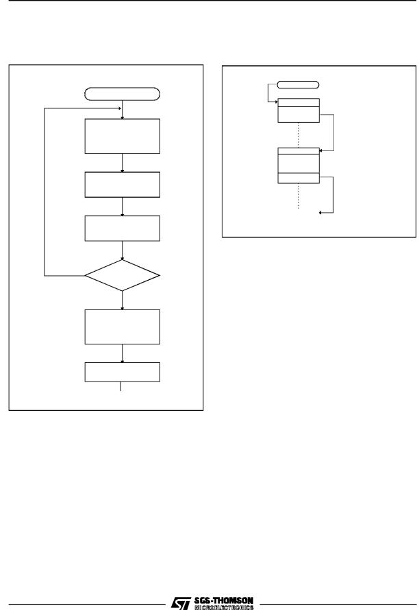
RESET (Continued)
Figure 21. Reset & Interrupt Processing
Flow-Chart
|
RESET |
|
NMI MASK SET |
|
INT LATCH CLEARED |
|
( IF PRESENT ) |
|
SELECT |
|
NMI MODE FLAGS |
|
PUT FFEh |
|
ON ADDRESS BUS |
YES |
IS RESET |
|
STILL PRESENT ? |
|
NO |
LOAD PC
FROM RESET LOCATIONS
FFE / FFF
FETCH INSTRUCTION
VA000427
ST63140,142,126,156
Figure 22. Restart Initialization Program
Flow-Chart
RESET
JP |
JP: 2 BYTES/4 CYCLES |
RESET VECTOR
INITIALIZATION
ROUTINE
RETI |
RETI: 1BYTES/2 CYCLES |
VA 000181
MCU Initialization Sequence
When a reset occurs the stack is reset to the program counter, the PC is loaded with the address of the reset vector (located in the program ROM at addresses FFEh & FFFh). A jump instruction to the beginning of the program has to be written into these locations. After a reset a NMI is automatically activated so that the core is in non-maskable interrupt mode to prevent false or ghost interrupts during the restart phase. Therefore the restart routine should be terminated by a RETI instruction to switch to normal mode and enable interrupts. If no pending interrupt is present at the end of the reset routine the ST631xx will continue with the instruction after the RETI; otherwise the pending interrupt will be serviced.
21/82

ST63140,142,126,156
WAIT & STOP MODES
The STOP and WAIT modes have been implemented in the ST631xx Core in order to reduce the consumption of the device when the latter has no instruction to execute. These two modes are described in the following paragraphs. On ST631xx as the hardware activated digital watchdog function is present the STOP instruction is de-activated and any attempt to execute it will cause the automatic execution of a WAIT instruction.
WAIT Mode
The configuration of the MCU in the WAIT mode occurs as soon as the WAIT instruction is executed. The microcontroller can also be considered as being in a ªsoftware frozenº state where the Core stops processing the instructions of the routine, the contents of the RAM locations and peripheral registers are saved as long as the power supply voltage is higher than the RAM retention voltage but where the peripherals are still working. The WAIT mode is used when the user wants to reduce the consumption of the MCU when it is in idle, while not losing count of time or monitoring of external events. The oscillator is not stopped in order to provide clock signal to the peripherals. The timers counting may be enabled (writing the PSI bit in TSCR register) and the timer interrupt may be also enabled before entering the WAIT mode; this allows the WAIT mode to be left when timer interrupt occurs. If the exit from the WAIT mode is performed with a general RESET (either from the activation of the external pin or by watchdog reset) the MCU will enter a normal reset procedure as described in the RESET chapter. If an interrupt is generated during WAIT mode the MCU behaviour depends on the state of the ST631xx Core before the initialization of the WAIT sequence, but also of the kind of the interrupt request that is generated. This case will be described in the following paragraphs. In any case, the ST631xx Core does not generate any delay after the occurrence of the interrupt because the oscillator clock is still available.
STOP Mode
On ST631xx the hardware watchdog is present and the STOP instruction has been de-activated. Any attempt to execute a STOP will cause the automatic execution of a WAIT instruction.
Exit from WAIT Mode
The following paragraphs describe the output procedure of the ST631xx Core from WAIT mode when an interrupt occurs. It must be noted that the restart sequence depends on the original state of
the MCU (normal, interrupt or non-maskable interrupt mode) before the start of the WAIT sequence, but also of the type of the interrupt request that is generated. In all cases the GEN bit of IOR has to be set to 1 in order to restart from WAIT Mode. Contrary to the operation of NMI in the RUN Mode, the NMI is masked in WAIT Mode if GEN=0.
Normal Mode. If the ST631xx Core was in the main routine when the WAIT instruction has been executed, the ST631xx Core outputs from the wait mode as soon as any interrupt occurs; the related interrupt routine is executed and at the end of the interrupt service routine the instruction that follows the WAIT instruction is executed if no other interrupts are pending.
Non-maskable Interrupt Mode. If the WAIT instruction has been executed during the execution of the non-maskable interrupt routine, the ST631xx Core outputs from the wait mode as soon as any interrupt occurs: the instruction that follows the WAIT instruction is executed and the ST631xx Core is still in the non-maskable interrupt mode even if another interrupt has been generated.
Normal Interrupt Mode. If the ST631xx Core was in the interrupt mode before the initialization of the WAIT sequence, it outputs from the wait mode as soon as any interrupt occurs. Nevertheless, two cases have to be considered:
-If the interrupt is a normal interrupt, the interrupt routine in which the WAIT was entered will be completed with the execution of the instruction that follows the WAIT and the ST631xx Core is still in the interrupt mode. At the end of this routine pending interrupts will be serviced in accordance to their priority.
-If the interrupt is a non-maskable interrupt, the non-maskable routine is processed at first. Then, the routine in which the WAIT was entered will be completed with the execution of the instruction that follows the WAIT and the ST631xx Core is still in the normal interrupt mode.
Notes :
If all the interrupt sources are disabled, the restart of the MCU can only be done by a Reset activation. The Wait instruction is not executed if an enabled interrupt request is pending. In the ST631xx the hardware activated digital watchdog function is present. As the watchdog is always activated the STOP instruction is de-activated and any attempt to execute the STOP instruction will cause an execution of a WAIT instruction.
22/82
 Loading...