SGS Thomson Microelectronics SM15T27A, SM15T27CA, SM15T30A, SM15T30CA, SM15T33A Datasheet
...
|
SM15T6V8A/220A |
|
SM15T6V8CA/220CA |
TRANSILTM
FEATURES
PEAK PULSE POWER : 1500 W (10/1000μs)
BREAKDOWN VOLTAGE RANGE :
From 6.8 V to 220 V
UNI AND BIDIRECTIONAL TYPES
LOW CLAMPING FACTOR
FAST RESPONSE TIME
UL RECOGNIZED
DESCRIPTION
Transil diodes provide high overvoltage protection by clamping action. Their instantane ous response to transient overvoltages makes them particularly suited to protect voltage sensitive devices such as MOS Technology and low voltage supplied IC's.
ABSOLUTE MAXIMUM RATINGS (Tamb = 25°C)
Symbol |
Parameter |
SMC
Value Unit
PPP |
Peak pulse power dissipation (see note1) |
Tj initial = Tamb |
1500 |
W |
P |
Power dissipation on infinite heatsink |
Tamb = 50°C |
6.5 |
W |
IFSM |
Non repetitive surge peak forward |
tp = 10ms |
200 |
A |
|
current for unidirectional types |
Tj initial = Tamb |
|
|
Tstg |
Storage temperature range |
|
- 65 to + 175 |
°C |
Tj |
Maximum junction temperature |
|
150 |
°C |
TL |
Maximum lead temperature for soldering during 10 s. |
260 |
°C |
|
Note 1 : For a surge greater than the maximum values, the diode will fail in short-circuit.
THERMAL RESISTANCES
Symbol
Rth (j-l)
Rth (j-a)
Parameter |
Value |
Unit |
Junction to leads |
15 |
°C/W |
Junction to ambient on printed circuit on recommended pad |
75 |
°C/W |
layout |
|
|
August 1999 Ed : 2A |
1/5 |

SM15Txx |
|
|
ELECTRICAL CHARACTERISTICS |
I |
|
(Tamb = 25°C) |
|
|
|
IF |
|
|
|
|
Symbol |
Parameter |
|
VRM |
Stand-off voltage |
|
|
|
|
VBR |
Breakdown voltage |
|
|
|
|
VCL |
Clamping voltage |
|
|
|
|
IRM |
Leakage current @ VRM |
|
|
||
IPP |
Peak pulse current |
|
|
|
|
αT |
Voltage temperature coefficient |
|
|||
VF |
Forward Voltage drop |
|
|
||
|
Types |
|
IRM @ VRM |
||
|
|
max |
|
||
|
|
|
|
|
|
Uni |
Mar- |
Bi |
Mar- |
μA |
V |
directional |
king |
directional |
king |
|
|
SM15T6V8A |
MDE |
SM15T6V8CA |
BDE |
1000 |
5.8 |
SM15T7V5A |
MDG |
SM15T7V5CA |
BDG |
500 |
6.4 |
SM15T10A |
MDP |
SM15T10CA |
NDP |
10 |
8.55 |
SM15T12A |
MDT |
SM15T12CA |
BDT |
5 |
10.2 |
SM15T15A |
MDX |
SM15T15CA |
BDX |
5 |
12.8 |
SM15T18A |
MEE |
SM15T18CA |
BEE |
5 |
15.3 |
SM15T22A |
MEK |
SM15T22CA |
BEK |
5 |
18.8 |
SM15T24A |
MEM |
SM15T24CA |
BEM |
5 |
20.5 |
SM15T27A |
MEP |
SM15T27CA |
BEP |
5 |
23.1 |
SM15T30A |
MER |
SM15T30CA |
BER |
5 |
25.6 |
SM15T33A |
MET |
SM15T33CA |
BET |
5 |
28.2 |
SM15T36A |
MEV |
SM15T36CA |
BEV |
5 |
30.8 |
SM15T39A |
MEX |
SM15T39CA |
BEX |
5 |
33.3 |
SM15T68A |
MFP |
SM15T68CA |
BFP |
5 |
58.1 |
SM15T100A |
MFX |
SM15T100CA |
BFX |
5 |
85.5 |
SM15T150A |
MGK |
SM15T150CA |
BGK |
5 |
128 |
SM15T200A |
MGV |
SM15T200CA |
BGV |
5 |
171 |
SM15T220A |
MGX |
SM15T220CA |
BGX |
5 |
188 |
% IPP |
|
|
|
|
|
10 0 |
10 |
s |
|
|
|
|
|
|
|
|
|
VCL VBR
VRM |
V F |
|
V |
|
I RM |
I PP
|
VBR |
@ IR |
|
VCL @ IPP |
VCL @ IPP |
αT C |
|||
min |
nom |
max |
|
max |
|
max |
|
max |
typ |
|
note2 |
|
10/1000μs |
8/20μs |
note3 note4 |
||||
V |
V |
V |
mA |
V |
A |
V |
A 10-4/°C pF |
||
6.45 |
6.8 |
7.14 |
10 |
10.5 |
143 |
13.4 |
746 |
5.7 |
9500 |
7.13 |
7.5 |
7.88 |
10 |
11.3 |
132 |
14.5 |
690 |
6.1 |
8500 |
9.5 |
10 |
10.5 |
1 |
14.5 |
103 |
18.6 |
538 |
7.3 |
7000 |
11.4 |
12 |
12.6 |
1 |
16.7 |
90 |
21.7 |
461 |
7.8 |
6000 |
14.3 |
15 |
15.8 |
1 |
21.2 |
71 |
27.2 |
368 |
8.4 |
5000 |
17.1 |
18 |
18.9 |
1 |
25.2 |
59.5 |
32.5 |
308 |
8.8 |
4300 |
20.9 |
22 |
23.1 |
1 |
30.6 |
49 |
39.3 |
254 |
9.2 |
3700 |
22.8 |
24 |
25.2 |
1 |
33.2 |
45 |
42.8 |
234 |
9.4 |
3500 |
25.7 |
27 |
28.4 |
1 |
37.5 |
40 |
48.3 |
207 |
9.6 |
3200 |
28.5 |
30 |
31.5 |
1 |
41.5 |
36 |
53.5 |
187 |
9.7 |
2900 |
31.4 |
33 |
34.7 |
1 |
45.7 |
33 |
59.0 |
169 |
9.8 |
2700 |
34.2 |
36 |
37.8 |
1 |
49.9 |
30 |
64.3 |
156 |
9.9 |
2500 |
37.1 |
39 |
41.0 |
1 |
53.9 |
28 |
69.7 |
143 |
10.0 |
2400 |
64.6 |
68 |
71.4 |
1 |
92 |
16.3 |
121 |
83 |
10.4 |
1550 |
95.0 |
100 |
105 |
1 |
137 |
11 |
178 |
56 |
10.6 |
1150 |
143 |
150 |
158 |
1 |
207 |
7.2 |
265 |
38 |
10.8 |
850 |
190 |
200 |
210 |
1 |
274 |
5.5 |
353 |
28 |
10.8 |
675 |
209 |
220 |
231 |
1 |
328 |
4.6 |
388 |
26 |
10.8 |
625 |
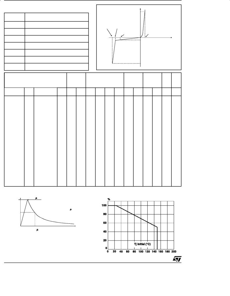
Fig. 1: Peak pulse power dissipation versus initial junction temperature (printed circuit board).
|
PULSE WAVEFORM 10/10 00 s |
50 |
|
0 |
t |
|
100 0 s |
Note 2 : |
Pulse test: tp < 50 ms. |
Note 3 : |
VBR = αT * (Tamb - 25) * VBR(25°C). |
Note 4 : |
VR = 0 V, F = 1 MHz. For bidirectional types, |
|
capacitance value is divided by 2. |
2/5
 Loading...