


SGS Thomson Microelectronics ST72T512R4, ST72T532R4, ST72T511R9, ST72T511R7, ST72T311R9 Datasheet
...ST72311R, ST72511R,
ST72512R, ST72532R
8-BIT MCU WITH NESTED INTERRUPTS, EEPROM, ADC, 16-BIT TIMERS, 8-BIT PWM ART, SPI, SCI, CAN INTERFACES
■Memories
±16K to 60K bytes Program memory (ROM,OTP and EPROM)
with read-out protection
±256 bytes E2PROM Data memory (only on ST72532R4)
±1024 to 2048 bytes RAM
■Clock, Reset and Supply Management
±Enhanced reset system
±Low voltage supply supervisor
±Clock sources: crystal/ceramic resonator oscillator or external clock
±Beep and Clock-out capability
±4 Power Saving Modes: Halt, Active-Halt, Wait and Slow
■Interrupt Management
±Nested interrupt controller
±13 interrupt vectors plus TRAP and RESET
±15 external interrupt lines (on 4 vectors)
±TLI dedicated top level interrupt pin
■48 I/O Ports
±48 multifunctional bidirectional I/O lines
±32 alternate function lines
±12 high sink outputs
■5 Timers
±Configurable watchdog timer
±Real time clock timer
±One 8-bit auto-reload timer with 4 independent PWM output channels, 2 input captures, output compares and external clock with event detector (except on ST725x2R4)
±Two 16-bit timers with: 2 input captures, 2 output compares, external clock input on one timer, PWM and Pulse generator modes
DATASHEET
TQFP64 14 x 14
■3 Communications Interfaces
±SPI synchronous serial interface
±SCI asynchronous serial interface
±CAN interface (except on ST72311Rx)
■1 Analog peripheral
±8-bit ADC with 8 input channels
■Instruction Set
±8-bit data manipulation
±63 basic instructions
±17 main addressing modes
±8 x 8 unsigned multiply instruction
±True bit manipulation
■Development Tools
±Full hardware/software development package
Device Summary
Features
Program memory - bytes RAM (stack) - bytes EEPROM - bytes
Peripherals
Operating Supply
CPU Frequency
Operating Temperature
Packages
ST72511R9 |
ST72511R7 |
ST72511R6 |
ST72311R9 |
ST72311R7 |
ST72311R6 |
ST72512R4 |
ST72532R4 |
60K |
48K |
32K |
60K |
48K |
32K |
16K |
16K |
2048 (256) |
1536 (256) |
1024 (256) |
2048 (256) |
1536 (256) |
1024 (256) |
1024 (256) |
1024 (256) |
- |
- |
- |
- |
- |
- |
- |
256 |
watchdog, two 16-bit timers, 8-bit PWM |
watchdog, two 16-bit timers, 8-bit PWM |
watchdog, two 16-bit timers, |
|||||
ART, SPI, SCI, CAN, ADC |
ART, SPI, SCI, ADC |
SPI, SCI, CAN, ADC |
|||||
|
|
|
3.0V to 5.5V |
|
|
|
3.0 to 5.5V 1) |
|
|
2 to 8 MHz (with 4 to 16 MHz oscillator) |
|
|
2 to 4 MHz 1) |
||
|
|
-40°C to +85°C (-40°C to +105/125°C optional) |
|
|
|||
|
|
|
TQFP64 |
|
|
|
|
Note 1. See Section 12.3.1 on page 133 for more information on VDD versus fOSC.
Rev. 2.1
February 2000 |
1/164 |

Table of Contents
1 GENERAL DESCRIPTION . . . . . . . . . . . . . . . . . . . . . . . . . . . . . . . . . . . . . . . . . . . . . . . . . |
. . . . . 6 |
||
1.1 |
INTRODUCTION . . . . . . . . . . . . . . . . . . . . . . . . . . . . . . . . . . . . . . . . . . . . . . . . . . . |
. . . . . 6 |
|
1.2 |
PIN DESCRIPTION . . . . . . . . . . . . . . . . . . . . . . . . . . . . . . . . . . . . . . . . . . . . . . . . . |
. . . . . 7 |
|
1.3 |
REGISTER & MEMORY MAP . . . . . . . . . . . . . . . . . . . . . . . . . . . . . . . . . . . . . . . . . |
. . . . 11 |
|
2 EPROM PROGRAM MEMORY . . . . . . . . . . . . . . . . . . . . . . . . . . . . . . . . . . . . . . . . . . . . . . |
. . . . 15 |
||
3 DATA EEPROM . . . . . . . . . . . . . . . . . . . . . . . . . . . . . . . . . . . . . . . . . . . . . . . . . . . . . . . . . |
. . . . 16 |
||
3.1 |
INTRODUCTION . . . . . . . . . . . . . . . . . . . . . . . . . . . . . . . . . . . . . . . . . . . . . . . . . . . |
. . . . 16 |
|
3.2 |
MAIN FEATURES . . . . . . . . . . . . . . . . . . . . . . . . . . . . . . . . . . . . . . . . . . . . . . . . . . |
. . . . 16 |
|
3.3 |
MEMORY ACCESS . . . . . . . . . . . . . . . . . . . . . . . . . . . . . . . . . . . . . . . . . . . . . . . . . |
. . . . 17 |
|
3.4 |
POWER SAVING MODES . . . . . . . . . . . . . . . . . . . . . . . . . . . . . . . . . . . . . . . . . . . |
. . . . 18 |
|
3.5 |
ACCESS ERROR HANDLING . . . . . . . . . . . . . . . . . . . . . . . . . . . . . . . . . . . . . . . . |
. . . . 18 |
|
3.6 |
REGISTER DESCRIPTION . . . . . . . . . . . . . . . . . . . . . . . . . . . . . . . . . . . . . . . . . . . |
. . . . 19 |
|
4 CENTRAL PROCESSING UNIT . . . . . . . . . . . . . . . . . . . . . . . . . . . . . . . . . . . . . . . . . . . . . |
. . . . 20 |
||
4.1 |
INTRODUCTION . . . . . . . . . . . . . . . . . . . . . . . . . . . . . . . . . . . . . . . . . . . . . . . . . . . |
. . . . 20 |
|
4.2 |
MAIN FEATURES . . . . . . . . . . . . . . . . . . . . . . . . . . . . . . . . . . . . . . . . . . . . . . . . . . |
. . . . 20 |
|
4.3 |
CPU REGISTERS . . . . . . . . . . . . . . . . . . . . . . . . . . . . . . . . . . . . . . . . . . . . . . . . . . |
. . . . 20 |
|
5 SUPPLY, RESET AND CLOCK MANAGEMENT . . . . . . . . . . . . . . . . . . . . . . . . . . . . . . . . |
. . . . 23 |
||
5.1 |
LOW VOLTAGE DETECTOR (LVD) . . . . . . . . . . . . . . . . . . . . . . . . . . . . . . . . . . . . |
. . . . 24 |
|
5.2 |
RESET SEQUENCE MANAGER (RSM) . . . . . . . . . . . . . . . . . . . . . . . . . . . . . . . . . |
. . . . 25 |
|
|
5.2.1 |
Introduction . . . . . . . . . . . . . . . . . . . . . . . . . . . . . . . . . . . . . . . . . . . . . . . . . . . |
. . . . 25 |
|
5.2.2 |
Asynchronous External RESET pin . . . . . . . . . . . . . . . . . . . . . . . . . . . . . . . . |
. . . . 26 |
|
5.2.3 |
Internal Low Voltage Detection RESET . . . . . . . . . . . . . . . . . . . . . . . . . . . . . |
. . . . 26 |
|
5.2.4 |
Internal Watchdog RESET . . . . . . . . . . . . . . . . . . . . . . . . . . . . . . . . . . . . . . . |
. . . . 26 |
5.3 |
LOW CONSUMPTION OSCILLATOR . . . . . . . . . . . . . . . . . . . . . . . . . . . . . . . . . . . |
. . . . 27 |
|
6 INTERRUPTS . . . . . . . . . . . . . . . . . . . . . . . . . . . . . . . . . . . . . . . . . . . . . . . . . . . . . . . . . . . |
. . . . 28 |
||
6.1 |
INTRODUCTION . . . . . . . . . . . . . . . . . . . . . . . . . . . . . . . . . . . . . . . . . . . . . . . . . . . |
. . . . 28 |
|
6.2 |
MASKING AND PROCESSING FLOW . . . . . . . . . . . . . . . . . . . . . . . . . . . . . . . . . . |
. . . . 28 |
|
6.3 |
INTERRUPTS AND LOW POWER MODES . . . . . . . . . . . . . . . . . . . . . . . . . . . . . . |
. . . . 30 |
|
6.4 |
CONCURRENT & NESTED MANAGEMENT . . . . . . . . . . . . . . . . . . . . . . . . . . . . . . |
. . . 30 |
|
6.5 |
INTERRUPT REGISTER DESCRIPTION . . . . . . . . . . . . . . . . . . . . . . . . . . . . . . . . . |
. . . 31 |
|
7 POWER SAVING MODES . . . . . . . . . . . . . . . . . . . . . . . . . . . . . . . . . . . . . . . . . . . . . . . . . . |
. . . 34 |
||
7.1 |
INTRODUCTION . . . . . . . . . . . . . . . . . . . . . . . . . . . . . . . . . . . . . . . . . . . . . . . . . . . . |
. . . 34 |
|
7.2 |
SLOW MODE . . . . . . . . . . . . . . . . . . . . . . . . . . . . . . . . . . . . . . . . . . . . . . . . . . . . . . |
. . . 34 |
|
7.3 |
WAIT MODE . . . . . . . . . . . . . . . . . . . . . . . . . . . . . . . . . . . . . . . . . . . . . . . . . . . . . . . |
. . . 35 |
|
7.4 |
ACTIVE-HALT AND HALT MODES . . . . . . . . . . . . . . . . . . . . . . . . . . . . . . . . . . . . . |
. . . 36 |
|
|
7.4.1 |
ACTIVE-HALT MODE . . . . . . . . . . . . . . . . . . . . . . . . . . . . . . . . . . . . . . . . . . . . |
. . . 36 |
|
7.4.2 |
HALT MODE . . . . . . . . . . . . . . . . . . . . . . . . . . . . . . . . . . . . . . . . . . . . . . . . . . . |
. . . 37 |
8 I/O PORTS . |
. . . . . . . . . . . . . . . . . . . . . . . . . . . . . . . . . . . . . . . . . . . . . . . . . . . . . . . . . . . . . . |
. . . 38 |
|
8.1 |
INTRODUCTION . . . . . . . . . . . . . . . . . . . . . . . . . . . . . . . . . . . . . . . . . . . . . . . . . . . . |
. . . 38 |
|
8.2 |
FUNCTIONAL DESCRIPTION . . . . . . . . . . . . . . . . . . . . . . . . . . . . . . . . . . . . . . . . . |
. . . 38 |
|
|
8.2.1 |
Input Modes . . . . . . . . . . . . . . . . . . . . . . . . . . . . . . . . . . . . . . . . . . . . . . . . . . . |
164. . . 38 |
|
8.2.2 |
Output Modes . . . . . . . . . . . . . . . . . . . . . . . . . . . . . . . . . . . . . . . . . . . . . . . . . . |
. . . 38 |
|
8.2.3 |
Alternate Functions . . . . . . . . . . . . . . . . . . . . . . . . . . . . . . . . . . . . . . . . . . . . . . |
. . . 38 |
2/164

Table of Contents
8.3 I/O PORT IMPLEMENTATION . . . . . . . . . . . . . . . . . . . . . . . . . . . . . . . . . . . . . . . . . . . . 41 8.4 LOW POWER MODES . . . . . . . . . . . . . . . . . . . . . . . . . . . . . . . . . . . . . . . . . . . . . . . . . . 42 8.5 INTERRUPTS . . . . . . . . . . . . . . . . . . . . . . . . . . . . . . . . . . . . . . . . . . . . . . . . . . . . . . . . . 42 8.5.1 Register Description . . . . . . . . . . . . . . . . . . . . . . . . . . . . . . . . . . . . . . . . . . . . . . . . 43
9 MISCELLANEOUS REGISTERS . . . . . . . . . . . . . . . . . . . . . . . . . . . . . . . . . . . . . . . . . . . . . . . . |
45 |
|
9.1 |
I/O PORT INTERRUPT SENSITIVITY . . . . . . . . . . . . . . . . . . . . . . . . . . . . . . . . . . . . . . |
45 |
9.2 I/O PORT ALTERNATE FUNCTIONS . . . . . . . . . . . . . . . . . . . . . . . . . . . . . . . . . . . . . . . |
45 |
|
9.3 |
MISCELLANEOUS REGISTERS . . . . . . . . . . . . . . . . . . . . . . . . . . . . . . . . . . . . . . . . . . |
46 |
10 ON-CHIP PERIPHERALS . . . . . . . . . . . . . . . . . . . . . . . . . . . . . . . . . . . . . . . . . . . . . . . . . . . . . |
49 |
|
10.1 |
WATCHDOG TIMER (WDG) . . . . . . . . . . . . . . . . . . . . . . . . . . . . . . . . . . . . . . . . . . . . . . |
49 |
|
10.1.1 Introduction . . . . . . . . . . . . . . . . . . . . . . . . . . . . . . . . . . . . . . . . . . . . . . . . . . . . . . . |
49 |
|
10.1.2 Main Features . . . . . . . . . . . . . . . . . . . . . . . . . . . . . . . . . . . . . . . . . . . . . . . . . . . . . |
49 |
|
10.1.3 Functional Description . . . . . . . . . . . . . . . . . . . . . . . . . . . . . . . . . . . . . . . . . . . . . . |
49 |
|
10.1.4 Hardware Watchdog Option . . . . . . . . . . . . . . . . . . . . . . . . . . . . . . . . . . . . . . . . . . |
50 |
|
10.1.5 Low Power Modes . . . . . . . . . . . . . . . . . . . . . . . . . . . . . . . . . . . . . . . . . . . . . . . . . |
50 |
|
10.1.6 Interrupts . . . . . . . . . . . . . . . . . . . . . . . . . . . . . . . . . . . . . . . . . . . . . . . . . . . . . . . . . |
50 |
|
10.1.7 Register Description . . . . . . . . . . . . . . . . . . . . . . . . . . . . . . . . . . . . . . . . . . . . . . . . |
50 |
10.2 MAIN CLOCK CONTROLLER WITH REAL TIME CLOCK TIMER (MCC/RTC) . . . . . . . |
52 |
|
|
10.2.1 Programmable CPU Clock Prescaler . . . . . . . . . . . . . . . . . . . . . . . . . . . . . . . . . . . |
52 |
|
10.2.2 Clock-out Capability . . . . . . . . . . . . . . . . . . . . . . . . . . . . . . . . . . . . . . . . . . . . . . . . |
52 |
|
10.2.3 Real Time Clock Timer (RTC) . . . . . . . . . . . . . . . . . . . . . . . . . . . . . . . . . . . . . . . . |
52 |
|
10.2.4 Register Description . . . . . . . . . . . . . . . . . . . . . . . . . . . . . . . . . . . . . . . . . . . . . . . . |
53 |
|
10.2.5 Low Power Modes . . . . . . . . . . . . . . . . . . . . . . . . . . . . . . . . . . . . . . . . . . . . . . . . . |
53 |
|
10.2.6 Interrupts . . . . . . . . . . . . . . . . . . . . . . . . . . . . . . . . . . . . . . . . . . . . . . . . . . . . . . . . . |
53 |
10.3 |
PWM AUTO-RELOAD TIMER (ART) . . . . . . . . . . . . . . . . . . . . . . . . . . . . . . . . . . . . . . . |
54 |
10.3.1 Introduction . . . . . . . . . . . . . . . . . . . . . . . . . . . . . . . . . . . . . . . . . . . . . . . . . . . . . . . 54
10.3.2 Functional Description . . . . . . . . . . . . . . . . . . . . . . . . . . . . . . . . . . . . . . . . . . . . . . 55
10.3.3 Register Description . . . . . . . . . . . . . . . . . . . . . . . . . . . . . . . . . . . . . . . . . . . . . . . . 58
10.4 16-BIT TIMER . . . . . . . . . . . . . . . . . . . . . . . . . . . . . . . . . . . . . . . . . . . . . . . . . . . . . . . . . 61
10.4.1 Introduction . . . . . . . . . . . . . . . . . . . . . . . . . . . . . . . . . . . . . . . . . . . . . . . . . . . . . . . |
61 |
10.4.2 Main Features . . . . . . . . . . . . . . . . . . . . . . . . . . . . . . . . . . . . . . . . . . . . . . . . . . . . . |
61 |
10.4.3 Functional Description . . . . . . . . . . . . . . . . . . . . . . . . . . . . . . . . . . . . . . . . . . . . . . |
61 |
10.4.4 Low Power Modes . . . . . . . . . . . . . . . . . . . . . . . . . . . . . . . . . . . . . . . . . . . . . . . . . |
73 |
10.4.5 Interrupts . . . . . . . . . . . . . . . . . . . . . . . . . . . . . . . . . . . . . . . . . . . . . . . . . . . . . . . . |
73 |
10.4.6 Summary of Timer modes . . . . . . . . . . . . . . . . . . . . . . . . . . . . . . . . . . . . . . . . . . . |
73 |
10.4.7 Register Description . . . . . . . . . . . . . . . . . . . . . . . . . . . . . . . . . . . . . . . . . . . . . . . . |
74 |
10.5 SERIAL PERIPHERAL INTERFACE (SPI) . . . . . . . . . . . . . . . . . . . . . . . . . . . . . . . . . . . |
79 |
10.5.1 Introduction . . . . . . . . . . . . . . . . . . . . . . . . . . . . . . . . . . . . . . . . . . . . . . . . . . . . . . . |
79 |
10.5.2 Main Features . . . . . . . . . . . . . . . . . . . . . . . . . . . . . . . . . . . . . . . . . . . . . . . . . . . . . |
79 |
10.5.3 General description . . . . . . . . . . . . . . . . . . . . . . . . . . . . . . . . . . . . . . . . . . . . . . . . . |
79 |
10.5.4 Functional Description . . . . . . . . . . . . . . . . . . . . . . . . . . . . . . . . . . . . . . . . . . . . . . |
81 |
10.5.5 Low Power Modes . . . . . . . . . . . . . . . . . . . . . . . . . . . . . . . . . . . . . . . . . . . . . . . . . |
88 |
10.5.6 Interrupts . . . . . . . . . . . . . . . . . . . . . . . . . . . . . . . . . . . . . . . . . . . . . . . . . . . . . . . . |
88 |
10.5.7 Register Description . . . . . . . . . . . . . . . . . . . . . . . . . . . . . . . . . . . . . . . . . . . . . . . . |
89 |
3/164

ST72311R, ST72511R, ST72512R, ST72532R |
|
|
10.6 |
SERIAL COMMUNICATIONS INTERFACE (SCI) . . . . . . . . . . . . . . . . . . . . . . . . . . . . . |
. 92 |
|
10.6.1 Introduction . . . . . . . . . . . . . . . . . . . . . . . . . . . . . . . . . . . . . . . . . . . . . . . . . . . . . . |
. 92 |
|
10.6.2 Main Features . . . . . . . . . . . . . . . . . . . . . . . . . . . . . . . . . . . . . . . . . . . . . . . . . . . . . |
92 |
|
10.6.3 General Description . . . . . . . . . . . . . . . . . . . . . . . . . . . . . . . . . . . . . . . . . . . . . . . . |
92 |
|
10.6.4 Functional Description . . . . . . . . . . . . . . . . . . . . . . . . . . . . . . . . . . . . . . . . . . . . . . |
94 |
|
10.6.5 Low Power Modes . . . . . . . . . . . . . . . . . . . . . . . . . . . . . . . . . . . . . . . . . . . . . . . . . |
99 |
|
10.6.6 Interrupts . . . . . . . . . . . . . . . . . . . . . . . . . . . . . . . . . . . . . . . . . . . . . . . . . . . . . . . . . |
99 |
|
10.6.7 Register Description . . . . . . . . . . . . . . . . . . . . . . . . . . . . . . . . . . . . . . . . . . . . . . . |
100 |
10.7 |
CONTROLLER AREA NETWORK (CAN) . . . . . . . . . . . . . . . . . . . . . . . . . . . . . . . . . . . |
104 |
|
10.7.1 Introduction . . . . . . . . . . . . . . . . . . . . . . . . . . . . . . . . . . . . . . . . . . . . . . . . . . . . . . |
104 |
|
10.7.2 Main Features . . . . . . . . . . . . . . . . . . . . . . . . . . . . . . . . . . . . . . . . . . . . . . . . . . . . |
105 |
|
10.7.3 Functional Description . . . . . . . . . . . . . . . . . . . . . . . . . . . . . . . . . . . . . . . . . . . . . |
105 |
|
10.7.4 Register Description . . . . . . . . . . . . . . . . . . . . . . . . . . . . . . . . . . . . . . . . . . . . . . . |
111 |
10.8 |
8-BIT A/D CONVERTER (ADC) . . . . . . . . . . . . . . . . . . . . . . . . . . . . . . . . . . . . . . . . . . |
121 |
|
10.8.1 Introduction . . . . . . . . . . . . . . . . . . . . . . . . . . . . . . . . . . . . . . . . . . . . . . . . . . . . . . |
121 |
|
10.8.2 Main Features . . . . . . . . . . . . . . . . . . . . . . . . . . . . . . . . . . . . . . . . . . . . . . . . . . . . |
121 |
|
10.8.3 Functional Description . . . . . . . . . . . . . . . . . . . . . . . . . . . . . . . . . . . . . . . . . . . . . |
121 |
|
10.8.4 Low Power Modes . . . . . . . . . . . . . . . . . . . . . . . . . . . . . . . . . . . . . . . . . . . . . . . . |
122 |
|
10.8.5 Interrupts . . . . . . . . . . . . . . . . . . . . . . . . . . . . . . . . . . . . . . . . . . . . . . . . . . . . . . . . |
122 |
|
10.8.6 Register Description . . . . . . . . . . . . . . . . . . . . . . . . . . . . . . . . . . . . . . . . . . . . . . . |
123 |
11 INSTRUCTION SET . . . . . . . . . . . . . . . . . . . . . . . . . . . . . . . . . . . . . . . . . . . . . . . . . . . . . . . . |
125 |
|
11.1 |
ST7 ADDRESSING MODES . . . . . . . . . . . . . . . . . . . . . . . . . . . . . . . . . . . . . . . . . . . . . |
125 |
|
11.1.1 Inherent . . . . . . . . . . . . . . . . . . . . . . . . . . . . . . . . . . . . . . . . . . . . . . . . . . . . . . . . . |
126 |
|
11.1.2 Immediate . . . . . . . . . . . . . . . . . . . . . . . . . . . . . . . . . . . . . . . . . . . . . . . . . . . . . . . |
126 |
|
11.1.3 Direct . . . . . . . . . . . . . . . . . . . . . . . . . . . . . . . . . . . . . . . . . . . . . . . . . . . . . . . . . . |
126 |
|
11.1.4 Indexed (No Offset, Short, Long) . . . . . . . . . . . . . . . . . . . . . . . . . . . . . . . . . . . . . |
126 |
|
11.1.5 Indirect (Short, Long) . . . . . . . . . . . . . . . . . . . . . . . . . . . . . . . . . . . . . . . . . . . . . . |
126 |
|
11.1.6 Indirect Indexed (Short, Long) . . . . . . . . . . . . . . . . . . . . . . . . . . . . . . . . . . . . . . . |
127 |
|
11.1.7 Relative mode (Direct, Indirect) . . . . . . . . . . . . . . . . . . . . . . . . . . . . . . . . . . . . . . |
127 |
11.2 |
INSTRUCTION GROUPS . . . . . . . . . . . . . . . . . . . . . . . . . . . . . . . . . . . . . . . . . . . . . . . |
128 |
12 ELECTRICAL CHARACTERISTICS . . . . . . . . . . . . . . . . . . . . . . . . . . . . . . . . . . . . . . . . . . . . |
131 |
|
12.1 |
PARAMETER CONDITIONS . . . . . . . . . . . . . . . . . . . . . . . . . . . . . . . . . . . . . . . . . . . . . |
131 |
|
12.1.1 Minimum and Maximum values . . . . . . . . . . . . . . . . . . . . . . . . . . . . . . . . . . . . . . |
131 |
|
12.1.2 Typical values . . . . . . . . . . . . . . . . . . . . . . . . . . . . . . . . . . . . . . . . . . . . . . . . . . . . |
131 |
|
12.1.3 Typical curves . . . . . . . . . . . . . . . . . . . . . . . . . . . . . . . . . . . . . . . . . . . . . . . . . . . . |
131 |
|
12.1.4 Loading capacitor . . . . . . . . . . . . . . . . . . . . . . . . . . . . . . . . . . . . . . . . . . . . . . . . . |
131 |
|
12.1.5 Pin input voltage . . . . . . . . . . . . . . . . . . . . . . . . . . . . . . . . . . . . . . . . . . . . . . . . . . |
131 |
12.2 |
ABSOLUTE MAXIMUM RATINGS . . . . . . . . . . . . . . . . . . . . . . . . . . . . . . . . . . . . . . . . |
132 |
|
12.2.1 Voltage Characteristics . . . . . . . . . . . . . . . . . . . . . . . . . . . . . . . . . . . . . . . . . . . . |
132 |
|
12.2.2 Current Characteristics . . . . . . . . . . . . . . . . . . . . . . . . . . . . . . . . . . . . . . . . . . . . |
132 |
|
12.2.3 Thermal Characteristics . . . . . . . . . . . . . . . . . . . . . . . . . . . . . . . . . . . . . . . . . . . . |
132 |
12.3 |
OPERATING CONDITIONS . . . . . . . . . . . . . . . . . . . . . . . . . . . . . . . . . . . . . . . . . . . . . |
133 |
|
12.3.1 General Operating Conditions . . . . . . . . . . . . . . . . . . . . . . . . . . . . . . . . . . . . . . . |
133 |
|
12.3.2 Operating Conditions with Low Voltage Detector (LVD) . . . . . . . . . . . . . . . . . . . . |
134 |
12.4 |
SUPPLY CURRENT CHARACTERISTICS . . . . . . . . . . . . . . . . . . . . . . . . . . . . . . . . . . |
135 |
|
12.4.1 RUN and SLOW Modes . . . . . . . . . . . . . . . . . . . . . . . . . . . . . . . . . . . . . . . . . . . . |
135 |
|
12.4.2 WAIT and SLOW WAIT Modes . . . . . . . . . . . . . . . . . . . . . . . . . . . . . . . . . . . . . . |
136 |
4/164

|
ST72311R, ST72511R, ST72512R, ST72532R |
|
|
12.4.3 HALT and ACTIVE-HALT Modes . . . . . . . . . . . . . . . . . . . . . . . . . . . . . . . . . . . . |
137 |
|
12.4.4 Supply and Clock Managers . . . . . . . . . . . . . . . . . . . . . . . . . . . . . . . . . . . . . . . . . |
137 |
|
12.4.5 On-Chip Peripheral . . . . . . . . . . . . . . . . . . . . . . . . . . . . . . . . . . . . . . . . . . . . . . . |
137 |
12.5 |
CLOCK AND TIMING CHARACTERISTICS . . . . . . . . . . . . . . . . . . . . . . . . . . . . . . . . . |
138 |
|
12.5.1 General Timings . . . . . . . . . . . . . . . . . . . . . . . . . . . . . . . . . . . . . . . . . . . . . . . . . |
138 |
|
12.5.2 External Clock Source . . . . . . . . . . . . . . . . . . . . . . . . . . . . . . . . . . . . . . . . . . . . . |
138 |
|
12.5.3 Crystal and Ceramic Resonator Oscillators . . . . . . . . . . . . . . . . . . . . . . . . . . . . . |
138 |
12.6 |
MEMORY CHARACTERISTICS . . . . . . . . . . . . . . . . . . . . . . . . . . . . . . . . . . . . . . . . . . |
139 |
12.6.1 RAM and Hardware Registers . . . . . . . . . . . . . . . . . . . . . . . . . . . . . . . . . . . . . . . 139 12.6.2 EEPROM Data Memory . . . . . . . . . . . . . . . . . . . . . . . . . . . . . . . . . . . . . . . . . . . . 139 12.6.3 EPROM Program Memory . . . . . . . . . . . . . . . . . . . . . . . . . . . . . . . . . . . . . . . . . . 139 12.7 EMC CHARACTERISTICS . . . . . . . . . . . . . . . . . . . . . . . . . . . . . . . . . . . . . . . . . . . . . . 140
|
12.7.1 Functional EMS . . . . . . . . . . . . . . . . . . . . . . . . . . . . . . . . . . . . . . . . . . . . . . . . . . |
140 |
|
12.7.2 Absolute Electrical Sensitivity . . . . . . . . . . . . . . . . . . . . . . . . . . . . . . . . . . . . . . . . |
141 |
|
12.7.3 ESD Pin Protection Strategy . . . . . . . . . . . . . . . . . . . . . . . . . . . . . . . . . . . . . . . . . |
143 |
12.8 |
I/O PORT PIN CHARACTERISTICS . . . . . . . . . . . . . . . . . . . . . . . . . . . . . . . . . . . . . . . |
145 |
|
12.8.1 General Characteristics . . . . . . . . . . . . . . . . . . . . . . . . . . . . . . . . . . . . . . . . . . . . |
145 |
|
12.8.2 Output Driving Current . . . . . . . . . . . . . . . . . . . . . . . . . . . . . . . . . . . . . . . . . . . . . |
146 |
12.9 |
CONTROL PIN CHARACTERISTICS . . . . . . . . . . . . . . . . . . . . . . . . . . . . . . . . . . . . . . |
147 |
12.9.1 Asynchronous RESET Pin . . . . . . . . . . . . . . . . . . . . . . . . . . . . . . . . . . . . . . . . . . 147
12.9.2 VPP Pin . . . . . . . . . . . . . . . . . . . . . . . . . . . . . . . . . . . . . . . . . . . . . . . . . . . . . . . . 147
12.10 TIMER PERIPHERAL CHARACTERISTICS . . . . . . . . . . . . . . . . . . . . . . . . . . . . . . . . . 148
12.10.1Watchdog Timer . . . . . . . . . . . . . . . . . . . . . . . . . . . . . . . . . . . . . . . . . . . . . . . . . 148 12.10.28-Bit PWM-ART Auto-Reload Timer . . . . . . . . . . . . . . . . . . . . . . . . . . . . . . . . . . 148 12.10.316-Bit Timer . . . . . . . . . . . . . . . . . . . . . . . . . . . . . . . . . . . . . . . . . . . . . . . . . . . . . 148 12.11 COMMUNICATIONS INTERFACE CHARACTERISTICS . . . . . . . . . . . . . . . . . . . . . . . 149
12.11.1SPI - Serial Peripheral Interface . . . . . . . . . . . . . . . . . . . . . . . . . . . . . . . . . . . . . . 149
12.11.2SCI - Serial Communications Interface . . . . . . . . . . . . . . . . . . . . . . . . . . . . . . . . 151
12.11.3CAN - Controller Area Network Interface . . . . . . . . . . . . . . . . . . . . . . . . . . . . . . . 151
12.12 8-BIT ADC CHARACTERISTICS . . . . . . . . . . . . . . . . . . . . . . . . . . . . . . . . . . . . . . . . . 152
13 PACKAGE CHARACTERISTICS . . . . . . . . . . . . . . . . . . . . . . . . . . . . . . . . . . . . . . . . . . . . . . 154
13.1 PACKAGE MECHANICAL DATA . . . . . . . . . . . . . . . . . . . . . . . . . . . . . . . . . . . . . . . . . 154 13.2 THERMAL CHARACTERISTICS . . . . . . . . . . . . . . . . . . . . . . . . . . . . . . . . . . . . . . . . . . 155 13.3 SOLDERING AND GLUEABILITY INFORMATION . . . . . . . . . . . . . . . . . . . . . . . . . . . . 156 13.4 PACKAGE/SOCKET FOOTPRINT PROPOSAL . . . . . . . . . . . . . . . . . . . . . . . . . . . . . . 157
14 DEVICE CONFIGURATION AND ORDERING INFORMATION . . . . . . . . . . . . . . . . . . . . . . . 158
14.1 OPTION BYTES . . . . . . . . . . . . . . . . . . . . . . . . . . . . . . . . . . . . . . . . . . . . . . . . . . . . . . 158 14.2 DEVICE ORDERING INFORMATION AND TRANSFER OF CUSTOMER CODE . . . . 159 14.3 DEVELOPMENT TOOLS . . . . . . . . . . . . . . . . . . . . . . . . . . . . . . . . . . . . . . . . . . . . . . . 161
15 ST7 GENERIC APPLICATION NOTE . . . . . . . . . . . . . . . . . . . . . . . . . . . . . . . . . . . . . . . . . . |
162 |
16 SUMMARY OF CHANGES . . . . . . . . . . . . . . . . . . . . . . . . . . . . . . . . . . . . . . . . . . . . . . . . . . . |
163 |
5/164
ST72311R, ST72511R, ST72512R, ST72532R
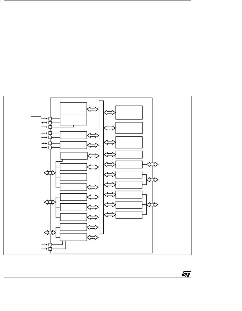
1 GENERAL DESCRIPTION
1.1 INTRODUCTION
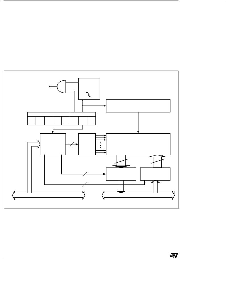
The ST72311R, ST72511R, ST72512R and ST72532R devices are members of the ST7 microcontroller family. They can be grouped as follows:
±ST725xxR devices are designed for mid-range applications with a CAN bus interface (Controller Area Network)
±ST72311R devices target the same range of applications but without CAN interface.
All devices are based on a common industrystandard 8-bit core, featuring an enhanced instruction set.
Figure 1. Device Block Diagram
RESET
VPP
TLI
VDD
VSS
OSC1
OSC2
PF7:0 (8-BIT)
PE7:0 (8-BIT)
PD7:0 (8-BIT)
VDDA
VSSA
8-BIT CORE
ALU
CONTROL
LVD
OSC
MCC/RTC
PORT F
TIMER A
BEEP
PORT E
CAN
SCI
PORT D
8-BIT ADC
Under software control, all devices can be placed in WAIT, SLOW, ACTIVE-HALT or HALT mode, reducing power consumption when the application is in idle or standby state.
The enhanced instruction set and addressing modes of the ST7 offer both power and flexibility to software developers, enabling the design of highly efficient and compact application code. In addition to standard 8-bit data management, all ST7 microcontrollers feature true bit manipulation, 8x8 unsigned multiplication and indirect addressing modes.
PROGRAM
MEMORY
(16K - 60K Bytes)
RAM
(1024, 2048 Bytes)
EEPROM
(256 Bytes)
ADDRESS |
PORT A |
PA7:0 |
|
WATCHDOG |
|
AND |
|
(8-BIT) |
PORT B |
|
|
DATA |
|
|
|
PB7:0 |
|
BUS |
|
(8-BIT) |
PWM ART |
|
|
|
|
|
|
PORT C |
|
|
TIMER B |
PC7:0 |
|
(8-BIT) |
|
|
|
|
|
SPI |
|
6/164

ST72311R, ST72511R, ST72512R, ST72532R
1.2 PIN DESCRIPTION
Figure 2. 64-Pin TQFP Package Pinout
|
PE3/ CANRX |
PE2/ CANTX |
PE1/ RDI |
PE0/ TDO |
V |
OSC1 |
OSC2 |
V |
TLI |
nc |
RESET |
V |
PA7(HS) |
PA6(HS) PA5(HS) |
PA4(HS) |
|
|
|
|
|
|
2 |
|
|
2 |
|
|
|
PP |
|
|
|
|
|
|
|
|
|
DD |
|
|
SS |
|
|
|
|
|
|
|
|
(HS) PE4 |
64 63 62 61 60 59 58 57 56 55 54 53 52 51 50 49 |
VSS_1 |
||||||||||||||
1 |
|
|
|
|
|
|
|
|
|
|
|
|
|
48 |
||
(HS) PE5 |
2 |
|
|
|
|
|
|
|
|
|
|
|
|
|
47 |
VDD_1 |
(HS) PE6 |
3 |
|
|
|
|
|
|
|
|
|
|
|
|
|
46 |
PA3 |
(HS) PE7 |
4 |
|
|
|
|
|
|
|
|
|
|
|
|
ei0 |
45 |
PA2 |
PWM3 / PB0 |
5 |
|
|
|
|
|
|
|
|
|
|
|
|
44 |
PA1 |
|
|
|
|
|
|
|
|
|
|
|
|
|
|
||||
PWM2 / PB1 |
6 |
ei2 |
|
|
|
|
|
|
|
|
|
|
|
|
43 |
PA0 |
PWM1 / PB2 |
7 |
|
|
|
|
|
|
|
|
|
|
|
|
42 |
PC7 / SS |
|
|
|
|
|
|
|
|
|
|
|
|
|
|
||||
PWM0 / PB3 |
8 |
|
|
|
|
|
|
|
|
|
|
|
|
|
41 |
PC6 / SCK |
ARTCLK / PB4 |
9 |
|
|
|
|
|
|
|
|
|
|
|
|
|
40 |
PC5 / MOSI |
PB5 |
10 |
ei3 |
|
|
|
|
|
|
|
|
|
|
|
|
39 |
PC4 / MISO |
PB6 |
11 |
|
|
|
|
|
|
|
|
|
|
|
|
38 |
PC3 (HS) / ICAP1_B |
|
PB7 |
12 |
|
|
|
|
|
|
|
|
|
|
|
|
|
37 |
PC2 (HS) / ICAP2_B |
AIN0 / PD0 |
13 |
|
|
|
|
|
|
|
|
|
|
|
|
|
36 |
PC1 / OCMP1_B |
AIN1 / PD1 |
14 |
|
|
|
|
|
|
|
|
|
|
|
|
|
35 |
PC0 / OCMP2_B |
AIN2 / PD2 |
15 |
|
|
|
|
|
|
|
|
ei1 |
|
|
|
|
34 |
VSS_0 |
AIN3 / PD3 |
16 |
|
|
|
|
|
|
|
|
|
|
|
|
|
33 |
VDD_0 |
|
17 18 19 20 21 22 23 24 25 26 27 28 29 30 31 32 |
|
||||||||||||||
|
AIN4 / PD4 |
AIN5 / PD5 |
AIN6 / PD6 |
AIN7 / PD7 |
DDA |
SSA |
DD 3 |
SS 3 |
MCO / PF0 |
BEEP / PF1 |
PF2 |
OCMP2 A / PF3 |
OCMP1 A / PF4 |
ICAP2 A / PF5 ICAP1 A / (HS) PF6 |
EXTCLK A / (HS) PF7 |
|
|
V |
V |
V |
V |
|
|||||||||||
(HS) |
20mA high sink capability |
eix |
associated external interrupt vector |
7/164
ST72311R, ST72511R, ST72512R, ST72532R
PIN DESCRIPTION (Cont'd)
For external pin connection guidelines, refer to Section 12 ºELECTRICAL CHARACTERISTICSº on page 131.
Legend / Abbreviations for Table 1:
Type: |
I = input, O = output, S = supply |
|
Input level: |
A = Dedicated analog input |
|
In/Output level: C = CMOS 0.3VDD/0.7VDD, |
||
|
|
CT= CMOS 0.3VDD/0.7VDD with input trigger |
Output level: |
HS = 20mA high sink (on N-buffer only) |
|
Port and control configuration: |
||
± |
Input: |
float = floating, wpu = weak pull-up, int = interrupt 1), ana = analog |
± |
Output: |
OD = open drain 2), PP = push-pull |
Refer to Section 8 ºI/O PORTSº on page 38 for more details on the software configuration of the I/O ports.
The RESET configuration of each pin is shown in bold. This configuration is valid as long as the device is in reset state.
Table 1. Device Pin Description
Pin n° |
|
Type |
Level |
|
TQFP64 |
Pin Name |
Input |
Output |
|
|
|
|
|
|
1 |
PE4 (HS) |
I/O |
CT |
HS |
2 |
PE5 (HS) |
I/O |
CT |
HS |
3 |
PE6 (HS) |
I/O |
CT |
HS |
4 |
PE7 (HS) |
I/O |
CT |
HS |
5 |
PB0/PWM3 |
I/O |
CT |
|
6 |
PB1/PWM2 |
I/O |
CT |
|
7 |
PB2/PWM1 |
I/O |
CT |
|
8 |
PB3/PWM0 |
I/O |
CT |
|
9 |
PB4/ARTCLK |
I/O |
CT |
|
10 |
PB5 |
I/O |
CT |
|
11 |
PB6 |
I/O |
CT |
|
12 |
PB7 |
I/O |
CT |
|
13 |
PD0/AIN0 |
I/O |
CT |
|
14 |
PD1/AIN1 |
I/O |
CT |
|
15 |
PD2/AIN2 |
I/O |
CT |
|
16 |
PD3/AIN3 |
I/O |
CT |
|
17 |
PD4/AIN4 |
I/O |
CT |
|
18 |
PD5/AIN5 |
I/O |
CT |
|
19 |
PD6/AIN6 |
I/O |
CT |
|
20 |
PD7/AIN7 |
I/O |
CT |
|
21 |
VDDA |
S |
|
|
22 |
VSSA |
S |
|
|
23 |
VDD_3 |
S |
|
|
float X
X X X X X X X X X X X X X X X X X X X
|
Port |
|
|
Main |
|
|
|
|
|
|
|
|
|
Inpu t |
|
Output |
function |
Alternate function |
||
|
(after |
|||||
wpu |
int |
ana |
OD |
PP |
|
|
reset) |
|
|||||
|
|
|
|
|
|
|
X |
|
|
X |
X |
Port E4 |
|
X |
|
|
X |
X |
Port E5 |
|
X |
|
|
X |
X |
Port E6 |
|
X |
|
|
X |
X |
Port E7 |
|
ei2 |
|
X |
X |
Port B0 |
PWM Output 3 |
|
ei2 |
|
X |
X |
Port B1 |
PWM Output 2 |
|
ei2 |
|
X |
X |
Port B2 |
PWM Output 1 |
|
|
ei2 |
|
X |
X |
Port B3 |
PWM Output 0 |
|
ei3 |
|
X |
X |
Port B4 |
PWM-ART External Clock |
ei3 |
|
X |
X |
Port B5 |
|
|
ei3 |
|
X |
X |
Port B6 |
|
|
ei3 |
|
X |
X |
Port B7 |
|
|
X |
|
X |
X |
X |
Port D0 |
ADC Analog Input 0 |
X |
|
X |
X |
X |
Port D1 |
ADC Analog Input 1 |
X |
|
X |
X |
X |
Port D2 |
ADC Analog Input 2 |
X |
|
X |
X |
X |
Port D3 |
ADC Analog Input 3 |
X |
|
X |
X |
X |
Port D4 |
ADC Analog Input 4 |
X |
|
X |
X |
X |
Port D5 |
ADC Analog Input 5 |
X |
|
X |
X |
X |
Port D6 |
ADC Analog Input 6 |
X |
|
X |
X |
X |
Port D7 |
ADC Analog Input 7 |
|
|
|
|
|
Analog Power Supply Voltage |
|
|
|
|
|
|
Analog Ground Voltage |
|
|
|
|
|
|
Digital Main Supply Voltage |
|
8/164

ST72311R, ST72511R, ST72512R, ST72532R
Pin n° |
|
Type |
Level |
float |
|
TQFP64 |
Pin Name |
Input |
Output |
||
|
|
|
|
|
|
24 |
VSS_3 |
S |
|
|
|
25 |
PF0/MCO |
I/O |
CT |
X |
|
26 |
PF1/BEEP |
I/O |
CT |
X |
|
27 |
PF2 |
I/O |
CT |
X |
|
28 |
PF3/OCMP2_A |
I/O |
CT |
X |
|
29 |
PF4/OCMP1_A |
I/O |
CT |
X |
|
30 |
PF5/ICAP2_A |
I/O |
CT |
X |
|
31 |
PF6 (HS)/ICAP1_A |
I/O |
CT |
HS |
X |
32 |
PF7 (HS)/EXTCLK_A I/O |
CT |
HS |
X |
|
33 |
VDD_0 |
S |
|
|
|
34 |
VSS_0 |
S |
|
|
|
35 |
PC0/OCMP2_B |
I/O |
CT |
X |
|
36 |
PC1/OCMP1_B |
I/O |
CT |
X |
|
37 |
PC2 (HS)/ICAP2_B |
I/O |
CT |
HS |
X |
38 |
PC3 (HS)/ICAP1_B |
I/O |
CT |
HS |
X |
39 |
PC4/MISO |
I/O |
CT |
X |
|
40 |
PC5/MOSI |
I/O |
CT |
X |
|
41 |
PC6/SCK |
I/O |
CT |
X |
|
42 |
PC7/SS |
I/O |
CT |
X |
|
43 |
PA0 |
I/O |
CT |
X |
|
44 |
PA1 |
I/O |
CT |
X |
|
45 |
PA2 |
I/O |
CT |
X |
|
46 |
PA3 |
I/O |
CT |
X |
|
47 |
VDD_1 |
S |
|
|
|
48 |
VSS_1 |
S |
|
|
|
49 |
PA4 (HS) |
I/O |
CT |
HS |
X |
50 |
PA5 (HS) |
I/O |
CT |
HS |
X |
51 |
PA6 (HS) |
I/O |
CT |
HS |
X |
52 |
PA7 (HS) |
I/O |
CT |
HS |
X |
53 |
VPP |
I |
|
|
|
54 |
RESET |
I/O |
|
C |
|
55 |
NC |
Not Connected |
|||
56 |
NMI |
I |
CT |
|
X |
57 |
VSS_3 |
S |
|
|
|
58 |
OSC2 3) |
I/O |
|
|
|
59 |
OSC1 3) |
I |
|
|
|
60 |
VDD_3 |
S |
|
|
|
|
Port |
|
Inpu t |
|
|
wpu |
int |
ana |
ei1
ei1
ei1
X
X
X
X
X
X
X
X
X
X
X
X
X ei0 ei0 ei0
ei0
X
X
X
|
|
Main |
|
|
Output |
function |
Alternate function |
||
(after |
||||
|
|
|
||
OD |
PP |
reset) |
|
|
|
|
|||
|
|
Digital Ground Voltage |
||
X |
X |
Port F0 |
Main clock output (fOSC/2) |
|
X |
X |
Port F1 |
Beep signal output |
|
X |
X |
Port F2 |
|
|
X |
X |
Port F3 |
Timer A Output Compare 2 |
|
X |
X |
Port F4 |
Timer A Output Compare 1 |
|
X |
X |
Port F5 |
Timer A Input Capture 2 |
|
X |
X |
Port F6 |
Timer A Input Capture 1 |
|
X |
X |
Port F7 |
Timer A External Clock Source |
|
|
|
Digital Main Supply Voltage |
||
|
|
Digital Ground Voltage |
||
X |
X |
Port C0 |
Timer B Output Compare 2 |
|
X |
X |
Port C1 |
Timer B Output Compare 1 |
|
X |
X |
Port C2 |
Timer B Input Capture 2 |
|
X |
X |
Port C3 |
Timer B Input Capture 1 |
|
X |
X |
Port C4 |
SPI Master In / Slave Out Data |
|
X |
X |
Port C5 |
SPI Master Out / Slave In Data |
|
X |
X |
Port C6 |
SPI Serial Clock |
|
X |
X |
Port C7 |
SPI Slave Select (active low) |
|
X |
X |
Port A0 |
|
|
X |
X |
Port A1 |
|
|
X |
X |
Port A2 |
|
|
X |
X |
Port A3 |
|
|
|
|
Digital Main Supply Voltage |
||
|
|
Digital Ground Voltage |
||
X |
X |
Port A4 |
|
|
X |
X |
Port A5 |
|
|
T |
|
Port A6 |
|
|
TPort A7
Must be tied low in user mode. In programming mode when available, this pin acts as the programming voltage input VPP .
XTop priority non maskable interrupt (active low)
Non maskable interrupt input pin Digital Ground Voltage
External clock mode input pull-up or crystal/ceramic resonator oscillator inverter output
External clock input or crystal/ceramic resonator oscillator inverter input
Digital Main Supply Voltage
9/164
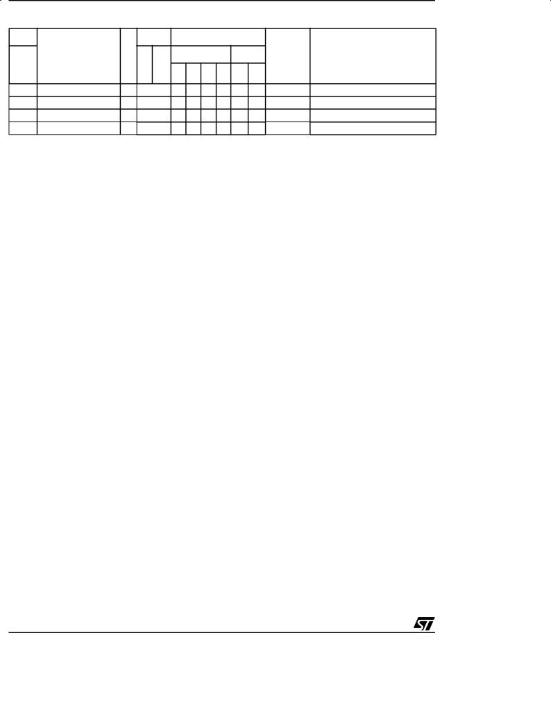
ST72311R, ST72511R, ST72512R, ST72532R
Pin n° |
|
TQFP64 |
Pin Name |
|
61 PE0/TDO
62 PE1/RDI
63 PE2/CANTX
64 PE3/CANRX
|
Level |
|
Type |
Input |
Output |
I/O |
|
CT |
I/O |
|
CT |
I/O |
|
CT |
I/O |
|
CT |
|
|
Port |
|
|
Inpu t |
|
|
float |
wpu |
int |
ana |
X |
X |
|
|
X |
X |
|
|
|
X |
|
|
X |
X |
|
|
|
|
Main |
|
|
Output |
function |
Alternate function |
||
(after |
||||
|
|
|
||
OD |
PP |
reset) |
|
|
|
|
|||
X |
X |
Port E0 |
SCI Transmit Data Out |
|
X |
X |
Port E1 |
SCI Receive Data In |
|
|
|
Port E2 |
CAN Transmit Data Output |
|
X |
X |
Port E3 |
CAN Receive Data Input |
|
Notes:
1. In the interrupt input column, ªeiXº defines the associated external interrupt vector. If the weak pull-up column (wpu) is merged with the interrupt column (int), then the I/O configuration is pull-up interrupt input, else the configuration is floating interrupt input.
2. In the open drain output column, ªTº defines a true open drain I/O (P-Buffer and protection diode to V
DD
are not implemented). See Section 8 ºI/O PORTSº on page 38 and Section 12.8 ºI/O PORT PIN CHARACTERISTICSº on page 145 for more details.
3. OSC1 and OSC2 pins connect a crystal/ceramic resonator or an external source to the on-chip oscillator see Section 1.2 ºPIN DESCRIPTIONº on page 7 and Section 12.5 ºCLOCK AND TIMING CHARACTERISTICSº on page 138 for more details.
10/164
ST72311R, ST72511R, ST72512R, ST72532R
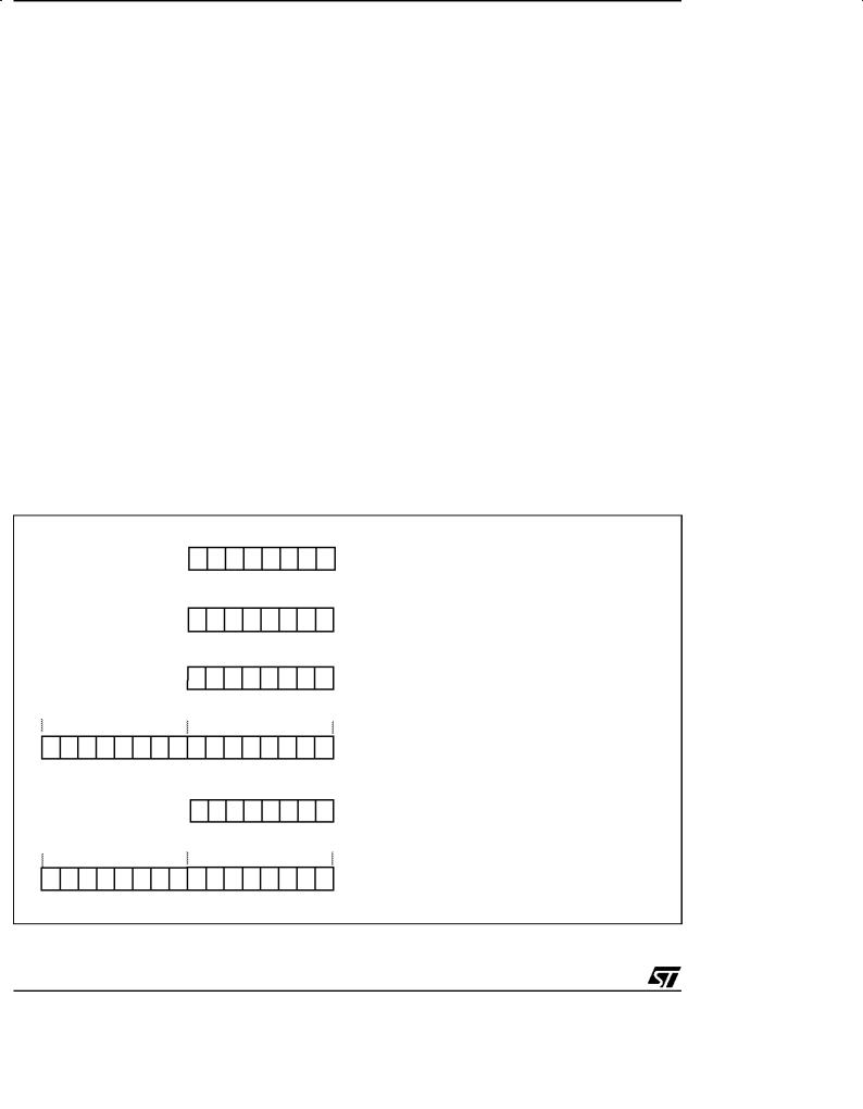
1.3 REGISTER & MEMORY MAP
As shown in the Figure 3, the MCU is capable of addressing 64K bytes of memories and I/O registers.
The available memory locations consist of 128 bytes of register location, up to 2Kbytes of RAM, up to 256 bytes of data EEPROM and up to
Figure 3. Memory Map
0000h |
HW Registers |
|
|
||
007Fh |
(see Table 2) |
|
|
||
0080h |
1024 Bytes RAM |
|
|
||
|
1536 Bytes RAM |
|
087Fh |
2048 Bytes RAM |
|
|
||
0880h |
Reserved |
|
0BFFh |
||
|
||
0C00h |
Optional EEPROM |
|
|
||
0CFFh |
(256 Bytes) |
|
|
||
0D00h |
Reserved |
|
|
0FFFh
1000h
Program Memory
(60K, 48K, 32K, 16K Bytes)
FFDFh
FFE0h
FFFF h
Interrupt & Reset Vectors
(see Table 7 on page 32)
60Kbytes of user program memory. The RAM space includes up to 256 bytes for the stack from 0100h to 01FFh.
The highest address bytes contain the user reset and interrupt vectors.
0080h
Short Addressing
RAM (zero page)
00FFh
0100h
Stack
(256 Bytes)
01FFh
0200h
16-bit Addressing
RAM
047Fh or 067Fh or 087Fh
1000h
60 KBytes
4000h
48 KBytes
8000h
32 KBytes
C000h
16 KBytes
FFFF h
11/164
ST72311R, ST72511R, ST72512R, ST72532R
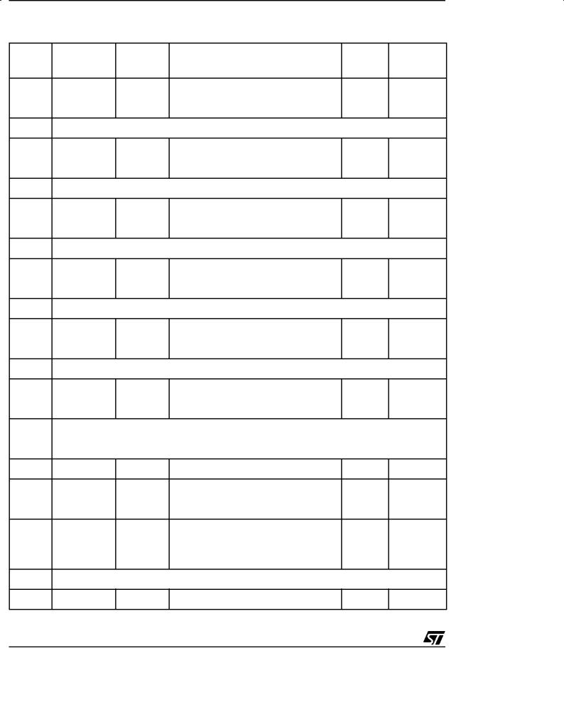
Table 2. Hardware Register Map
Address |
Block |
Register |
Register Name |
Reset |
Remarks |
|
Label |
Status |
|||||
|
|
|
|
|||
0000h |
|
PADR |
Port A Data Register |
00h 1) |
R/W |
|
0001h |
Port A |
PADDR |
Port A Data Direction Register |
00h |
R/W |
|
0002h |
|
PAOR |
Port A Option Register |
00h |
R/W 2) |
|
0003h |
|
|
Reserved Area (1 Byte) |
|
|
|
0004h |
|
PCDR |
Port C Data Register |
00h 1) |
R/W |
|
0005h |
Port C |
PCDDR |
Port C Data Direction Register |
00h |
R/W |
|
0006h |
|
PCOR |
Port C Option Register |
00h |
R/W |
|
0007h |
|
|
Reserved Area (1 Byte) |
|
|
|
0008h |
|
PBDR |
Port B Data Register |
00h 1) |
R/W |
|
0009h |
Port B |
PBDDR |
Port B Data Direction Register |
00h |
R/W |
|
000Ah |
|
PBOR |
Port B Option Register |
00h |
R/W |
|
000Bh |
|
|
Reserved Area (1 Byte) |
|
|
|
000Ch |
|
PEDR |
Port E Data Register |
00h 1) |
R/W |
|
000Dh |
Port E |
PEDDR |
Port E Data Direction Register |
00h |
R/W 2) |
|
000Eh |
|
PEOR |
Port E Option Register |
00h |
R/W 2) |
|
000Fh |
|
|
Reserved Area (1 Byte) |
|
|
|
0010h |
|
PDDR |
Port D Data Register |
00h 1) |
R/W |
|
0011h |
Port D |
PDDDR |
Port D Data Direction Register |
00h |
R/W |
|
0012h |
|
PDOR |
Port D Option Register |
00h |
R/W |
|
0013h |
|
|
Reserved Area (1 Byte) |
|
|
|
0014h |
|
PFDR |
Port F Data Register |
00h 1) |
R/W |
|
0015h |
Port F |
PFDDR |
Port F Data Direction Register |
00h |
R/W |
|
0016h |
|
PFOR |
Port F Option Register |
00h |
R/W |
|
0017h |
|
|
|
|
|
|
to |
|
|
Reserved Area (9 Bytes) |
|
|
|
001Fh |
|
|
|
|
|
|
0020h |
|
MISCR1 |
Miscellaneous Register 1 |
00h |
R/W |
|
0021h |
|
SPIDR |
SPI Data I/O Register |
xxh |
R/W |
|
0022h |
SPI |
SPICR |
SPI Control Register |
0xh |
R/W |
|
0023h |
|
SPISR |
SPI Status Register |
00h |
Read Only |
|
0024h |
|
ISPR0 |
Interrupt Software Priority Register 0 |
FFh |
R/W |
|
0025h |
ITC |
ISPR1 |
Interrupt Software Priority Register 1 |
FFh |
R/W |
|
0026h |
ISPR2 |
Interrupt Software Priority Register 2 |
FFh |
R/W |
||
|
||||||
0027h |
|
ISPR3 |
Interrupt Software Priority Register 3 |
FFh |
R/W |
|
0028h |
|
|
Reserved Area (1 Byte) |
|
|
|
0029h |
MCC |
MCCSR |
Main Clock Control / Status Register |
01h |
R/W |
12/164
ST72311R, ST72511R, ST72512R, ST72532R
Address |
Block |
|
002Ah |
WATCHDOG |
|
002Bh |
||
|
||
002Ch |
EEPROM |
|
002Dh |
|
|
to |
|
|
0030h |
|
|
0031h |
|
|
0032h |
|
|
0033h |
|
|
0034h |
|
|
0035h |
|
|
0036h |
|
|
0037h |
|
|
0038h |
TIMER A |
|
0039h |
|
|
003Ah |
|
|
003Bh |
|
|
003Ch |
|
|
003Dh |
|
|
003Eh |
|
|
003Fh |
|
|
0040h |
|
|
0041h |
|
|
0042h |
|
|
0043h |
|
|
0044h |
|
|
0045h |
|
|
0046h |
|
|
0047h |
|
|
0048h |
TIMER B |
|
0049h |
|
004Ah
004Bh
004Ch
004Dh
004Eh
004Fh
0050h |
|
|
0051h |
|
|
0052h |
|
|
0053h |
SCI |
|
0054h |
||
|
||
0055h |
|
|
0056h |
|
|
0057h |
|
Register |
Register Name |
Reset |
Remarks |
|
Label |
Status |
|||
|
|
|||
WDGCR |
Watchdog Control Register |
7Fh |
R/W |
|
WDGSR |
Watchdog Status Register |
000x 000x |
R/W |
|
EECSR |
Data EEPROM Control/Status Register |
00h |
R/W |
|
|
Reserved Area (4 Bytes) |
|
|
|
TACR2 |
Timer A Control Register 2 |
00h |
R/W |
|
TACR1 |
Timer A Control Register 1 |
00h |
R/W |
|
TASR |
Timer A Status Register |
xxh |
Read Only |
|
TAIC1HR |
Timer A Input Capture 1 High Register |
xxh |
Read Only |
|
TAIC1LR |
Timer A Input Capture 1 Low Register |
xxh |
Read Only |
|
TAOC1HR |
Timer A Output Compare 1 High Register |
80h |
R/W |
|
TAOC1LR |
Timer A Output Compare 1 Low Register |
00h |
R/W |
|
TACHR |
Timer A Counter High Register |
FFh |
Read Only |
|
TACLR |
Timer A Counter Low Register |
FCh |
Read Only |
|
TAACHR |
Timer A Alternate Counter High Register |
FFh |
Read Only |
|
TAACLR |
Timer A Alternate Counter Low Register |
FCh |
Read Only |
|
TAIC2HR |
Timer A Input Capture 2 High Register |
xxh |
Read Only |
|
TAIC2LR |
Timer A Input Capture 2 Low Register |
xxh |
Read Only |
|
TAOC2HR |
Timer A Output Compare 2 High Register |
80h |
R/W |
|
TAOC2LR |
Timer A Output Compare 2 Low Register |
00h |
R/W |
|
MISCR2 |
Miscellaneous Register 2 |
00h |
R/W |
|
TBCR2 |
Timer B Control Register 2 |
00h |
R/W |
|
TBCR1 |
Timer B Control Register 1 |
00h |
R/W |
|
TBSR |
Timer B Status Register |
xxh |
Read Only |
|
TBIC1HR |
Timer B Input Capture 1 High Register |
xxh |
Read Only |
|
TBIC1LR |
Timer B Input Capture 1 Low Register |
xxh |
Read Only |
|
TBOC1HR |
Timer B Output Compare 1 High Register |
80h |
R/W |
|
TBOC1LR |
Timer B Output Compare 1 Low Register |
00h |
R/W |
|
TBCHR |
Timer B Counter High Register |
FFh |
Read Only |
|
TBCLR |
Timer B Counter Low Register |
FCh |
Read Only |
|
TBACHR |
Timer B Alternate Counter High Register |
FFh |
Read Only |
|
TBACLR |
Timer B Alternate Counter Low Register |
FCh |
Read Only |
|
TBIC2HR |
Timer B Input Capture 2 High Register |
xxh |
Read Only |
|
TBIC2LR |
Timer B Input Capture 2 Low Register |
xxh |
Read Only |
|
TBOC2HR |
Timer B Output Compare 2 High Register |
80h |
R/W |
|
TBOC2LR |
Timer B Output Compare 2 Low Register |
00h |
R/W |
|
SCISR |
SCI Status Register |
C0h |
Read Only |
|
SCIDR |
SCI Data Register |
xxh |
R/W |
|
SCIBRR |
SCI Baud Rate Register |
00xx xxxx |
R/W |
|
SCICR1 |
SCI Control Register 1 |
xxh |
R/W |
|
SCICR2 |
SCI Control Register 2 |
00h |
R/W |
|
SCIERPR |
SCI Extended Receive Prescaler Register |
00h |
R/W |
|
|
Reserved area |
|
|
|
SCIETPR |
SCI Extended Transmit Prescaler Register |
00h |
R/W |
13/164
ST72311R, ST72511R, ST72512R, ST72532R
Address |
Block |
Register |
Register Name |
Reset |
Remarks |
|
Label |
Status |
|||||
|
|
|
|
|||
0058h |
|
|
Reserved Area (2 Bytes) |
|
|
|
0059h |
|
|
|
|
||
|
|
|
|
|
||
005Ah |
|
CANISR |
CAN Interrupt Status Register |
00h |
R/W |
|
005Bh |
|
CANICR |
CAN Interrupt Control Register |
00h |
R/W |
|
005Ch |
|
CANCSR |
CAN Control / Status Register |
00h |
R/W |
|
005Dh |
|
CANBRPR |
CAN Baud Rate Prescaler Register |
00h |
R/W |
|
005Eh |
CAN |
CANBTR |
CAN Bit Timing Register |
23h |
R/W |
|
005Fh |
|
CANPSR |
CAN Page Selection Register |
00h |
R/W |
|
0060h |
|
|
First address |
|
See CAN |
|
to |
|
|
to |
|
Description |
|
006Fh |
|
|
Last address of CAN page X |
|
|
|
0070h |
ADC |
ADCDR |
Data Register |
xxh |
Read Only |
|
0071h |
ADCCSR |
Control/Status Register |
00h |
R/W |
||
|
||||||
0072h |
|
PWMDCR3 |
PWM AR Timer Duty Cycle Register 3 |
00h |
R/W |
|
0073h |
|
PWMDCR2 |
PWM AR Timer Duty Cycle Register 2 |
00h |
R/W |
|
0074h |
|
PWMDCR1 |
PWM AR Timer Duty Cycle Register 1 |
00h |
R/W |
|
0075h |
PWM ART |
PWMDCR0 |
PWM AR Timer Duty Cycle Register 0 |
00h |
R/W |
|
0076h |
PWMCR |
PWM AR Timer Control Register |
00h |
R/W |
||
|
||||||
0077h |
|
ARTCSR |
Auto-Reload Timer Control/Status Register |
00h |
R/W |
|
0078h |
|
ARTCAR |
Auto-Reload Timer Counter Access Register |
00h |
R/W |
|
0079h |
|
ARTARR |
Auto-Reload Timer Auto-Reload Register |
00h |
R/W |
|
007Ah |
|
|
|
|
|
|
to |
|
|
Reserved Area (6 Bytes) |
|
|
|
007Fh |
|
|
|
|
|
Legend: x=undefined, R/W=read/write
Notes:
1.The contents of the I/O port DR registers are readable only in output configuration. In input configuration, the values of the I/O pins are returned instead of the DR register contents.
2.The bits associated with unavailable pins must always keep their reset value.
14/164

ST72311R, ST72511R, ST72512R, ST72532R
2 EPROM PROGRAM MEMORY
The program memory of the OTP and EPROM devices can be programmed with EPROM programming tools available from STMicroelectronics
EPROM Erasure
EPROM devices are erased by exposure to high intensity UV light admitted through the transparent window. This exposure discharges the floating gate to its initial state through induced photo current.
It is recommended that the EPROM devices be kept out of direct sunlight, since the UV content of
sunlight can be sufficient to cause functional failure. Extended exposure to room level fluorescent lighting may also cause erasure.
An opaque coating (paint, tape, label, etc...) should be placed over the package window if the product is to be operated under these lighting conditions. Covering the window also reduces IDD in power-saving modes due to photo-diode leakage currents.
15/164
ST72311R, ST72511R, ST72512R, ST72532R
3 DATA EEPROM
3.1 INTRODUCTION
The Electrically Erasable Programmable Read Only Memory can be used as a non volatile backup for storing data. Using the EEPROM requires a basic access protocol described in this chapter.
Figure 4. EEPROM Block Diagram
3.2 MAIN FEATURES
■Up to 16 Bytes programmed in the same cycle
■EEPROM mono-voltage (charge pump)
■Chained erase and programming cycles
■Internal control of the global programming cycle duration
■End of programming cycle interrupt flag
■WAIT mode management
FALLING
EEPROM INTERRUPT EDGE
DETECTOR
|
|
|
|
|
HIGH VOLTAGE |
|
|
|
|
|
|
|
PUMP |
EECSR |
RESERVED |
|
EEPROM |
|
||
0 0 |
0 0 |
IE |
LAT |
PGM |
|
|
0 |
|
|||||
|
ADDRESS |
4 |
|
EEPROM |
||
|
ROW |
|
||||
|
DECODER |
|
|
MEMORY MATRIX |
||
|
|
DECODER |
|
|||
|
|
|
|
|
(1 ROW = 16 x 8 BITS) |
|
|
|
|
|
|
128 |
128 |
|
|
|
|
4 |
DATA |
16 x 8 BITS |
|
|
|
|
|
MULTIPLEXER |
DATA LATCHES |
|
|
|
|
4 |
|
|
|
ADDRESS BUS |
|
|
DATA BUS |
||
16/164
ST72311R, ST72511R, ST72512R, ST72532R
DATA EEPROM (Cont'd)
3.3 MEMORY ACCESS
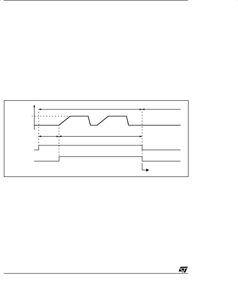
The Data EEPROM memory read/write access modes are controlled by the LAT bit of the EEPROM Control/Status register (EECSR). The flowchart in Figure 5 describes these different memory access modes.
Read Operation (LAT=0)
The EEPROM can be read as a normal ROM location when the LAT bit of the EECSR register is cleared. In a read cycle, the byte to be accessed is put on the data bus in less than 1 CPU clock cycle. This means that reading data from EEPROM takes the same time as reading data from EPROM, but this memory cannot be used to execute machine code.
Write Operation (LAT=1)
To access the write mode, the LAT bit has to be set by software (the PGM bit remains cleared). When a write access to the EEPROM area occurs, the value is latched inside the 16 data latches according to its address.
Figure 5. Data EEPROM Programming Flowchart
When PGM bit is set by the software, all the previous bytes written in the data latches (up to 16) are programmed in the EEPROM cells. The effective high address (row) is determined by the last EEPROM write sequence. To avoid wrong programming, the user must take care that all the bytes written between two programming sequences have the same high address: only the four Least Significant Bits of the address can change.
At the end of the programming cycle, the PGM and LAT bits are cleared simultaneously, and an interrupt is generated if the IE bit is set. The Data EEPROM interrupt request is cleared by hardware when the Data EEPROM interrupt vector is fetched.
Note: Care should be taken during the programming cycle. Writing to the same memory location will over-program the memory (logical AND between the two write access data result) because the data latches are only cleared at the end of the programming cycle and by the falling edge of LAT bit.
It is not possible to read the latched data. This note is ilustrated by the Figure 6.
READ MODE |
|
WRITE MODE |
|
LAT=0 |
|
LAT=1 |
|
PGM=0 |
|
PGM=0 |
|
READ BYTES |
WRITE UP TO 16 BYTES |
||
IN EEPROM AREA |
|||
IN EEPROM AREA |
|||
(with the same 12 MSB of the address) |
|||
|
|||
|
START PROGRAMMING CYCLE |
||
|
|
LAT=1 |
|
|
PGM=1 (set by software) |
||
INTERRUPT GENERATION |
|
|
|
IF IE=1 |
0 |
1 |
|
|
|
LAT |
|
CLEARED BY HARDWARE
17/164
ST72311R, ST72511R, ST72512R, ST72532R
DATA EEPROM (Cont'd)
3.4 POWER SAVING MODES Wait mode
The DATA EEPROM can enter WAIT mode on execution of the WFI instruction of the microcontroller. The DATA EEPROM will immediately enter this mode if there is no programming in progress, otherwise the DATA EEPROM will finish the cycle and then enter WAIT mode.
Halt mode
The DATA EEPROM immediatly enters HALT mode if the microcontroller executes the HALT instruction. Therefore the EEPROM will stop the function in progress, and data may be corrupted.
3.5 ACCESS ERROR HANDLING
If a read access occurs while LAT=1, then the data bus will not be driven.
If a write access occurs while LAT=0, then the data on the bus will not be latched.
If a programming cycle is interrupted (by software/ RESET action), the memory data will not be guaranteed.
Figure 6. Data EEPROM Programming Cycle
READ OPERATION NOT POSSIBLE |
READ OPERATION POSSIBLE |
|
INTERNAL |
|
|
PROGRAMMING |
|
|
VOLTAGE |
|
|
ERASE CYCLE |
WRITE CYCLE |
|
WRITE OF
DATA LATCHES
tPROG
LAT
PGM
EEPROM INTERRUPT
18/164

ST72311R, ST72511R, ST72512R, ST72532R
DATA EEPROM (Cont'd)
3.6 REGISTER DESCRIPTION CONTROL/STATUS REGISTER (CSR)
Read/Write
Reset Value: 0000 0000 (00h)
7 |
0 |
Bit 1 = LAT Latch Access Transfer
This bit is set by software. It is cleared by hardware at the end of the programming cycle. It can only be cleared by software if PGM bit is cleared.
0:Read mode
1:Write mode
0 |
0 |
0 |
0 |
0 |
IE LAT PGM |
Bit 7:3 = Reserved, forced by hardware to 0.
Bit 2 = IE Interrupt enable
This bit is set and cleared by software. It enables the Data EEPROM interrupt capability when the PGM bit is cleared by hardware. The interrupt request is automatically cleared when the software enters the interrupt routine.
0:Interrupt disabled
1:Interrupt enabled
Bit 0 = PGM Programming control and status
This bit is set by software to begin the programming cycle. At the end of the programming cycle, this bit is clearedby hardware and an interrupt is generated if the ITE bit is set.
0:Programming finished or not yet started
1:Programming cycle is in progress
Note: if the PGM bit is cleared during the programming cycle, the memory data is not guaranteed
Table 3. DATA EEPROM Register Map and Reset Values
Address |
Register |
7 |
6 |
5 |
4 |
3 |
2 |
1 |
0 |
|
(Hex.) |
Label |
|||||||||
|
|
|
|
|
|
|
|
|||
002Ch |
EECSR |
|
|
|
|
|
IE |
RWM |
PGM |
|
Reset Value |
0 |
0 |
0 |
0 |
0 |
0 |
0 |
0 |
||
|
19/164
ST72311R, ST72511R, ST72512R, ST72532R
4 CENTRAL PROCESSING UNIT
4.1 INTRODUCTION
This CPU has a full 8-bit architecture and contains six internal registers allowing efficient 8-bit data manipulation.
4.2 MAIN FEATURES
■Enable executing 63 basic instructions
■Fast 8-bit by 8-bit multiply
■17 main addressing modes (with indirect addressing mode)
■Two 8-bit index registers
■16-bit stack pointer
■Low power HALT and WAIT modes
■Priority maskable hardware interrupts
■Non-maskable software/hardware interrupts
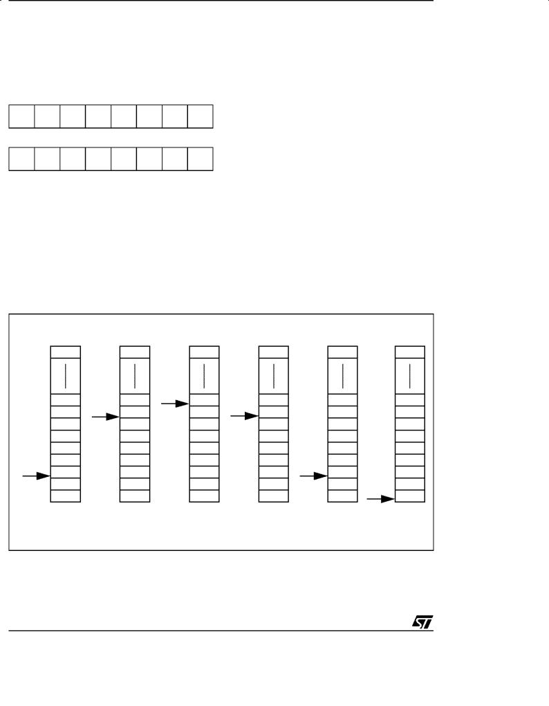
4.3 CPU REGISTERS
The 6 CPU registers shown in Figure 7 are not present in the memory mapping and are accessed by specific instructions.
Accumulator (A)
The Accumulator is an 8-bit general purpose register used to hold operands and the results of the arithmetic and logic calculations and to manipulate data.
Index Registers (X and Y)
These 8-bit registers are used to create effective addresses or as temporary storage areas for data manipulation. (The Cross-Assembler generates a precede instruction (PRE) to indicate that the following instruction refers to the Y register.)
The Y register is not affected by the interrupt automatic procedures.
Program Counter (PC)
The program counter is a 16-bit register containing the address of the next instruction to be executed by the CPU. It is made of two 8-bit registers PCL (Program Counter Low which is the LSB) and PCH (Program Counter High which is the MSB).
Figure 7. CPU Registers
|
|
|
7 |
|
|
|
|
|
|
0 |
|
|
|
|
|
|
|
|
|
|
|
|
ACCUMULATOR |
|
|
|
RESET VALUE = XXh |
|
|
||||||
|
|
|
7 |
|
|
|
|
|
|
0 |
|
|
|
|
|
|
|
|
|
|
|
|
X INDEX REGISTER |
|
|
|
RESET VALUE = XXh |
|
|
||||||
|
|
|
7 |
|
|
|
|
|
|
0 |
|
|
|
|
|
|
|
|
|
|
|
|
Y INDEX REGISTER |
|
|
|
RESET VALUE = XXh |
|
|
||||||
15 |
PCH |
8 |
7 |
|
|
PCL |
|
|
0 |
|
|
|
|
|
|
|
|
|
|
|
|
|
PROGRAM COUNTER |
RESET VALUE = RESET VECTOR @ FFFEh-FFFFh |
|
||||||||||
|
|
|
7 |
|
|
|
|
|
|
0 |
|
|
|
|
1 |
1 |
I1 |
H |
I0 |
N |
Z C |
CONDITION CODE REGISTER |
|
|
|
|
|
|
|
|
|
|
|
|
|
|
RESET VALUE = 1 |
1 |
1 |
X |
1 |
X |
X |
X |
|
||
15 |
|
8 |
7 |
|
|
|
|
|
|
0 |
|
|
|
|
|
|
|
|
|
|
|
|
STACK POINTER |
RESET VALUE = STACK HIGHER ADDRESS |
|
|
|
||||||||
X = Undefined Value
20/164
ST72311R, ST72511R, ST72512R, ST72532R
CENTRAL PROCESSING UNIT (Cont'd)
Condition Code Register (CC)
Read/Write
Reset Value: 111x1xxx
7 |
|
|
|
|
|
|
0 |
1 |
1 |
I1 |
H |
I0 |
N |
Z |
C |
The 8-bit Condition Code register contains the interrupt masks and four flags representative of the result of the instruction just executed. This register can also be handled by the PUSH and POP instructions.
These bits can be individually tested and/or controlled by specific instructions.
Arithmetic management bits
Bit 4 = H Half carry.
This bit is set by hardware when a carry occurs between bits 3 and 4 of the ALU during an ADD or ADC instructions. It is reset by hardware during the same instructions.
0:No half carry has occurred.
1:An half carry has occurred.
This bit is tested using the JRH or JRNH instruction. The H bit is useful in BCD arithmetic subroutines.
Bit 2 = N Negative.
This bit is set and cleared by hardware. It is representative of the result sign of the last arithmetic, logical or data manipulation. It's a copy of the result 7th bit.
0:The result of the last operation is positive or null.
1:The result of the last operation is negative
(i.e. the most significant bit is a logic 1).
This bit is accessed by the JRMI and JRPL instructions.
Bit 1 = Z Zero.
This bit is set and cleared by hardware. This bit indicates that the result of the last arithmetic, logical or data manipulation is zero.
0:The result of the last operation is different from zero.
1:The result of the last operation is zero.
This bit is accessed by the JREQ and JRNE test instructions.
Bit 0 = C Carry/borrow.
This bit is set and cleared by hardware and software. It indicates an overflow or an underflow has occurred during the last arithmetic operation.
0:No overflow or underflow has occurred.
1:An overflow or underflow has occurred.
This bit is driven by the SCF and RCF instructions and tested by the JRC and JRNC instructions. It is also affected by the ªbit test and branchº, shift and rotate instructions.
Interrupt management bits
Bit 5,3 = I1, I0 Interrupt.
The combination of the Iand I0 bits gives the current interrupt software priority.
Interrupt Software Priority |
I1 |
I0 |
|
Level 0 |
(main) |
1 |
0 |
Level 1 |
|
0 |
1 |
Level 2 |
|
0 |
0 |
Level 3 |
(= interrupt disable) |
1 |
1 |
These two bits are set/cleared by hardware when entering in interrupt. The loaded value is given by the corresponding bits in the interrupt software priority registers (IxSPR). They can be also set/ cleared by software with the RIM, SIM, IRET, HALT, WFI and PUSH/POP instructions.
See the interrupt management chapter for more details.
21/164
ST72311R, ST72511R, ST72512R, ST72532R
CENTRAL PROCESSING UNIT (Cont'd)
Stack Pointer (SP)
Read/Write
Reset Value: 01 FFh
15 |
|
|
|
|
|
|
8 |
0 |
0 |
0 |
0 |
0 |
0 |
0 |
1 |
7 |
|
|
|
|
|
|
0 |
SP7 |
SP6 |
SP5 |
SP4 |
SP3 |
SP2 |
SP1 |
SP0 |
The Stack Pointer is a 16-bit register which is always pointing to the next free location in the stack. It is then decremented after data has been pushed onto the stack and incremented before data is popped from the stack (see Figure 8).
Since the stack is 256 bytes deep, the 8 most significant bits are forced by hardware. Following an MCU Reset, or after a Reset Stack Pointer instruction (RSP), the Stack Pointer contains its reset value (the SP7 to SP0 bits are set) which is the stack higher address.
Figure 8. Stack Manipulation Example
CALL |
Interrupt |
PUSH Y |
Subroutine |
Event |
|
@ 0100h |
|
|
|
|
SP |
|
|
SP |
Y |
|
|
|
||
|
CC |
CC |
|
|
A |
A |
|
|
X |
X |
|
SP |
PCH |
PCH |
|
PCL |
PCL |
||
|
|||
PCH |
PCH |
PCH |
|
@ 01FFh PCL |
PCL |
PCL |
The least significant byte of the Stack Pointer (called S) can be directly accessed by a LD instruction.
Note: When the lower limit is exceeded, the Stack Pointer wraps around to the stack upper limit, without indicating the stack overflow. The previously stored information is then overwritten and therefore lost. The stack also wraps in case of an underflow.
The stack is used to save the return address during a subroutine call and the CPU context during an interrupt. The user may also directly manipulate the stack by means of the PUSH and POP instructions. In the case of an interrupt, the PCL is stored at the first location pointed to by the SP. Then the other registers are stored in the next locations as shown in Figure 8
±When an interrupt is received, the SP is decremented and the context is pushed on the stack.
±On return from interrupt, the SP is incremented and the context is popped from the stack.
A subroutine call occupies two locations and an interrupt five locations in the stack area.
POP Y |
IRET |
RET |
|
|
or RSP |
SP
CC |
|
|
A |
|
|
X |
|
|
PCH |
SP |
|
PCL |
||
|
||
PCH |
PCH |
|
PCL |
SP |
|
PCL |
Stack Higher Address = 01FFh Stack Lower Address = 0100h
22/164
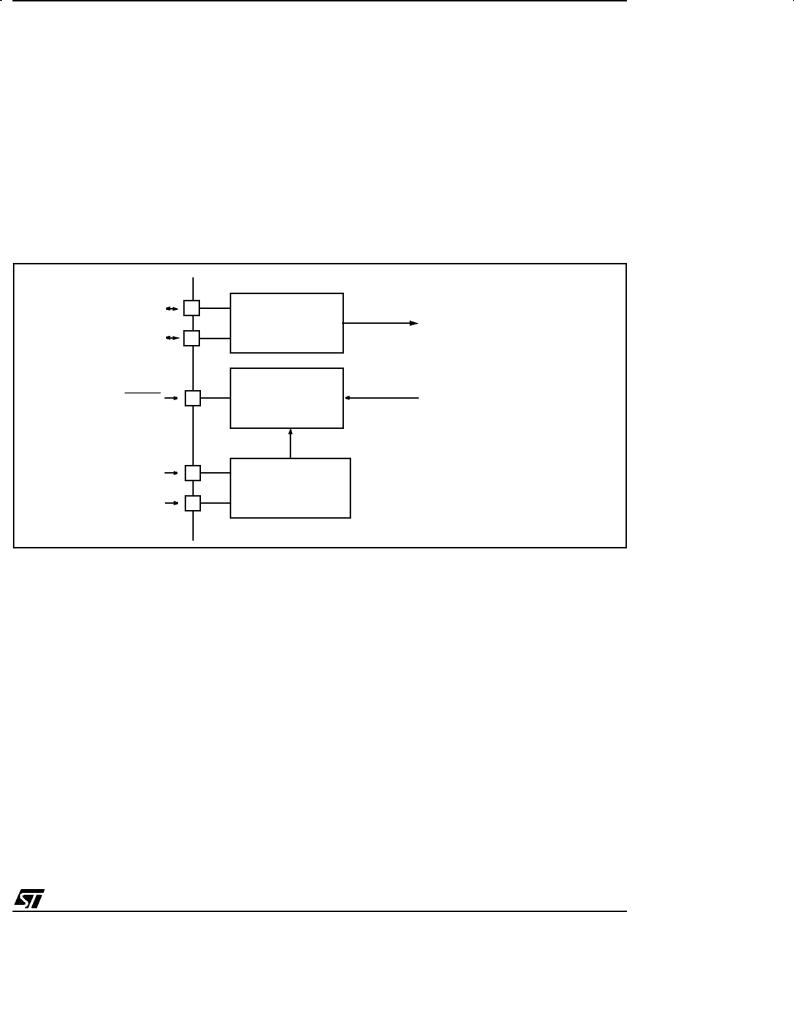
ST72311R, ST72511R, ST72512R, ST72532R
5 SUPPLY, RESET AND CLOCK MANAGEMENT
The ST72311R, ST72511R, ST72512R and ST72532R microcontrollers include a range of utility features for securing the application in critical situations (for example in case of a power brownout), and reducing the number of external components. An overview is shown in Figure 9.
Main features
■Main supply low voltage detection (LVD)
■RESET Manager (RSM)
■Low consumption resonator oscillator
Figure 9. Clock, RESET, Option and Supply Management Overview
OSC2 |
|
fOSC |
TO |
|
OSCILLATOR |
MAIN CLOCK |
|
OSC1 |
|
|
CONTROLLER |
|
|
|
|
RESET |
RESET |
|
FROM |
|
WATCHDOG |
||
|
|
|
PERIPHERAL |
VDD |
LOW VOLTAGE |
|
|
|
DETECTOR |
|
|
VSS |
(LVD) |
|
|
23/164
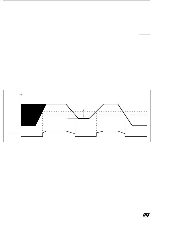
ST72311R, ST72511R, ST72512R, ST72532R
5.1 LOW VOLTAGE DETECTOR (LVD)
To allow the integration of power management features in the application, the Low Voltage Detector function (LVD) generates a static reset when the VDD supply voltage is below a VIT- reference value. This means that it secures the power-up as well as the power-down keeping the ST7 in reset.
The VIT- reference value for a voltage drop is lower than the VIT+ reference value for power-on in order to avoid a parasitic reset when the MCU starts running and sinks current on the supply (hysteresis).
The LVD Reset circuitry generates a reset when VDD is below:
±VIT+ when VDD is rising
±VIT- when VDD is falling
The LVD function is illustrated in Figure 10.
Provided the minimum VDD value (guaranteed for the oscillator frequency) is below VIT-, the MCU can only be in two modes:
Figure 10. Low Voltage Detector vs Reset
VDD
VIT+
VIT-
±under full software control
±in static safe reset
In these conditions, secure operation is always ensured for the application without the need for external reset hardware.
During a Low Voltage Detector Reset, the RESET pin is held low, thus permitting the MCU to reset other devices.
Notes:
The LVD allows the device to be used without any external RESET circuitry.
The LVD is an optional function which can be selected when ordering the device (ordering information).
Vhys
RESET
24/164
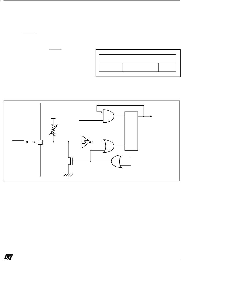
ST72311R, ST72511R, ST72512R, ST72532R
5.2 RESET SEQUENCE MANAGER (RSM)
5.2.1 Introduction
The reset sequence manager includes three RESET sources as shown in Figure 12:
■External RESET source pulse
■Internal LVD RESET (Low Voltage Detection)
■Internal WATCHDOG RESET
The 4096 CPU clock cycle delay allows the oscillator to stabilise and ensures that recovery has taken place from the Reset state.
The RESET vector fetch phase duration is 2 clock cycles.
Figure 11. RESET Sequence Phases
These sources act on the RESET pin and it is always kept low during the delay phase.
The RESET service routine vector is fixed at ad- |
|
RESET |
|
||
dresses FFFEh-FFFFh in the ST7 memory map. |
DELAY |
INTERNAL RESET |
FETCH |
||
The basic RESET sequence consists of 3 phases |
4096 CLOCK CYCLES |
VECTOR |
|||
|
|||||
|
|
|
|||
as shown in Figure 11: |
|
|
|
|
|
■ Delay depending on the RESET source |
|
|
|
|
|
■ 4096 CPU clock cycle delay |
|
|
|
|
|
■ RESET vector fetch |
|
|
|
|
|
Figure 12. Reset Block Diagram |
|
|
|
|
|
VDD |
fCPU |
|
|
INTERNAL |
|
|
|
|
RESET |
||
RON |
|
|
COUNTER |
|
|
|
|
|
|
||
RESET
WATCHDOG RESET
LVD RESET
25/164
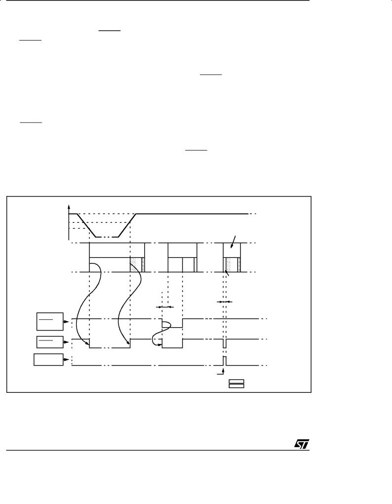
ST72311R, ST72511R, ST72512R, ST72532R
RESET SEQUENCE MANAGER (Cont'd)
5.2.2 Asynchronous External RESET pin
The RESET pin is both an input and an open-drain output with integrated RON weak pull-up resistor. This pull-up has no fixed value but varies in accordance with the input voltage. It can be pulled low by external circuitry to reset the device. See electrical characteristics section for more details.
A RESET signal originating from an external
source must have a duration of at least th(RSTL)in in order to be recognized as shown in Figure 13. This
detection is asynchronous and therefore the MCU can enter reset state even in HALT mode.
The RESET pin is an asynchronous signal which plays a major role in EMS performance. In a noisy environment, it is recommended to follow the guidelines mentioned in the electrical characteristics section.
5.2.3 Internal Low Voltage Detection RESET
Two different RESET sequences caused by the internal LVD circuitry can be distinguished:
■Power-On RESET
■Voltage Drop RESET
The device RESET pin acts as an output that is pulled low when VDD<VIT+ (rising edge) or VDD<VIT- (falling edge) as shown in Figure 13.
The LVD filters spikes on VDD larger than tg(VDD) to avoid parasitic resets.
5.2.4 Internal Watchdog RESET
The RESET sequence generated by a internal Watchdog counter overflow is shown in Figure 13.
Starting from the Watchdog counter underflow, the device RESET pin acts as an output that is pulled low during tw(RSTL)out.
CAUTION: this output signal as not enought energy to be used to drive external devices.
Figure 13. RESET Sequences
VDD
VIT+
VIT- |
|
|
WATCHDOG |
|
|
|
RESET |
|
LVD |
SHORT EXT. |
|
|
RESET |
RESET |
|
RUN |
RUN |
RUN |
RUN |
|
DELAY |
DELAY |
|
|
|
|
DELAY |
|
th(RSTL)in |
|
tw(RSTL)out |
EXTERNAL
RESET
SOURCE
RESET PIN
WATCHDOG
RESET
WATCHDOG UNDERFLOW
INTERNAL RESET (4096 TCP U)
FETCH VECTOR
26/164
ST72311R, ST72511R, ST72512R, ST72532R
5.3 LOW CONSUMPTION OSCILLATOR
The fOSC main clock of the ST7 can be generated by two different source types:
■an external source
■a crystal or ceramic resonator oscillators
The associated hardware configuration are shown in Table 4. Refer to the electrical characteristics section for more details.
External Clock Source
In this external clock mode, a clock signal (square, sinus or triangle) with ~50% duty cycle has to drive the OSC1 pin while the OSC2 pin is tied to ground.
Crystal/Ceramic Oscillator
This oscillator (based on constant current source) is optimized in terms of consumption and has the advantage of producing a very accurate rate on the main clock of the ST7.
When using this oscillator, the resonator and the load capacitances have to be connected as shown in Table 4 and have to be mounted as close as possible to the oscillator pins in order to minimize output distortion and start-up stabilization time.
This oscillator is not stopped during the RESET phase to avoid losing time in the oscillator start-up phase.
These oscillators are not stopped during the RESET phase to avoid losing time in the oscillator start-up phase.
Table 4. ST7 Clock Sources
|
Hardware Configur ation |
||
Clock |
ST7 |
VDD |
|
OSC1 |
OSC2 |
||
|
|||
External |
EXTERNAL |
ROBP |
|
|
|||
|
|
||
Resonators |
SOURCE |
|
|
ST7 |
|
||
|
|
||
Crystal/Ceramic |
OSC1 |
OSC2 |
|
CL1 |
CL2 |
||
LOAD
CAPACITORS
27/164
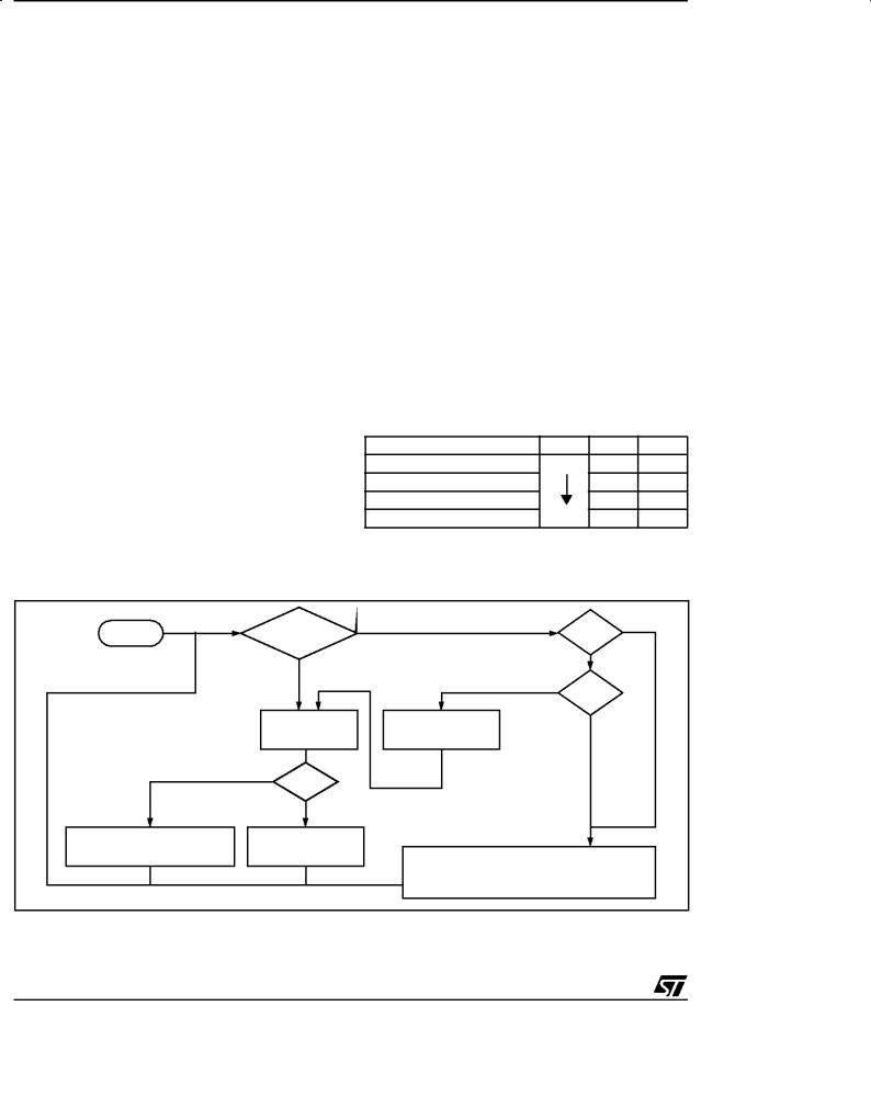
ST72311R, ST72511R, ST72512R, ST72532R
6 INTERRUPTS
6.1 INTRODUCTION
The ST7 enhanced interrupt management provides the following features:
■Hardware interrupts
■Software interrupt (TRAP)
■Nested or concurrent interrupt management with flexible interrupt priority and level management:
±Up to 4 software programmable nesting levels
±Up to 16 interrupt vectors fixed by hardware
±3 non maskable events: TLI, RESET, TRAP This interrupt management is based on:
±Bit 5 and bit 3 of the CPU CC register (I1:0),
±Interrupt software priority registers (ISPRx),
±Fixed interrupt vector addresses located at the high addresses of the memory map (FFE0h to FFFFh) sorted by hardware priority order.
This enhanced interrupt controller guarantees full upward compatibility with the standard (not nested) ST7 interrupt controller.
6.2 MASKING AND PROCESSING FLOW
The interrupt masking is managed by the I1 and I0 bits of the CC register and the ISPRx registers which give the interrupt software priority level of each interrupt vector (see Table 5). The processing flow is shown in Figure 14
Figure 14. Interrupt Processing Flowchart
When an interrupt request has to be serviced:
±Normal processing is suspended at the end of the current instruction execution.
±The PC, X, A and CC registers are saved onto the stack.
±I1 and I0 bits of CC register are set according to the corresponding values in the ISPRx registers
of the serviced interrupt vector.
± The PC is then loaded with the interrupt vector of the interrupt to service and the first instruction of the interrupt service routine is fetched (refer to ªInterrupt Mappingº table for vector addresses).
The interrupt service routine should end with the IRET instruction which causes the contents of the saved registers to be recovered from the stack.
Note: As a consequence of the IRET instruction, the I1 and I0 bits will be restored from the stack and the program in the previous level will resume.
Table 5. Interrupt Software Priority Levels
Interrupt software priority |
Level |
I1 |
I0 |
|
Level 0 |
(main) |
Low |
1 |
0 |
Level 1 |
|
|
0 |
1 |
Level 2 |
|
|
0 |
0 |
Level 3 |
(= interrupt disable) |
High |
1 |
1 |
RESET |
PENDIN G |
Y |
|
Y |
INTERRUPT |
|
|
TLI |
|
|
|
|
|
|
|
N |
|
Interrupt has the same or a |
N |
|
|
lower software priority |
|
|
|
|
|
than current one |
I1:0 |
|
|
|
|
|
FETCH NEXT |
|
INSTRUC TION |
|
Y |
|
ªIRETº |
|
N |
RESTORE PC, X, A, CC |
EXECUTE |
FROM STACK |
INSTRUCTI ON |
THE INTERRUPT |
softwarepriority currentthan one |
Interrupthas ahigher |
|
STAYS PENDING |
|
STACK PC, X, A, CC
LOAD I1:0 FROM INTERRUPT SW REG.
LOAD PC FROM INTERRUPT VECTOR
28/164
INTERRUPTS (Cont'd)
Servicing Pending Interrupts
As several interrupts can be pending at the same time, the interrupt to be taken into account is determined by the following two-step process:
±the highest software priority interrupt is serviced,
±if several interrupts have the same software priority then the interrupt with the highest hardware priority is serviced first.
Figure 15 describes this decision process.
Figure 15. Priority Decision Process
PENDING
INTERRUPTS
Same |
SOFTWARE |
Different |
|
PRIORITY |
|
HIGHEST SOFTWAR E
PRIORITY SERVIC ED
HIGHEST HARDWARE
PRIORITY SERVICED
When an interrupt request is not serviced immediately, it is latched and then processed when its software priority combined with the hardware priority becomes the highest one.
Note 1: The hardware priority is exclusive while the software one is not. This allows the previous process to succeed with only one interrupt.
Note 2: RESET, TRAP and TLI are non maskable and they can be considered as having the highest software priority in the decision process.
Different Interrupt Vector Sources
Two interrupt source types are managed by the ST7 interrupt controller: the non-maskable type (RESET, TLI, TRAP) and the maskable type (external or from internal peripherals).
Non-Maskable Sources
These sources are processed regardless of the state of the I1 and I0 bits of the CC register (see Figure 14). After stacking the PC, X, A and CC registers (except for RESET), the corresponding vector is loaded in the PC register and the I1 and
ST72311R, ST72511R, ST72512R, ST72532R
I0 bits of the CC are set to disable interrupts (level 3). These sources allow the processor to exit HALT mode.
■ TLI (Top Level Hardware Interrupt)
This hardware interrupt occurs when a specific edge is detected on the dedicated TLI pin. Its detailed specification is given in the Miscellaneous register chapter.
■ TRAP (Non Maskable Software Interrupt)
This software interrupt is serviced when the TRAP instruction is executed. It will be serviced according to the flowchart on Figure 14 as a TLI.
■ RESET
The RESET source has the highest priority in the ST7. This means that the first current routine has the highest software priority (level 3) and the highest hardware priority.
See the RESET chapter for more details.
Maskable Sources
Maskable interrupt vector sources can be serviced if the corresponding interrupt is enabled and if its own interrupt software priority (in ISPRx registers) is higher than the one currently being serviced (I1 and I0 in CC register). If any of these two conditions is false, the interrupt is latched and thus remains pending.
■ External Interrupts
External interrupts allow the processor to exit from HALT low power mode.
External interrupt sensitivity is software selectable through the Miscellaneous registers (MISCRx). External interrupt triggered on edge will be latched and the interrupt request automatically cleared upon entering the interrupt service routine.
If several input pins of a group connected to the same interrupt line are selected simultaneously, these will be logically ORed.
■ Peripheral Interrupts
Usually the peripheral interrupts cause the MCU to exit from HALT mode except those mentioned in the ªInterrupt Mappingº table.
A peripheral interrupt occurs when a specific flag is set in the peripheral status registers and if the corresponding enable bit is set in the peripheral control register.
The general sequence for clearing an interrupt is based on an access to the status register followed by a read or write to an associated register.
Note: The clearing sequence resets the internal latch. A pending interrupt (i.e. waiting for being serviced) will therefore be lost if the clear sequence is executed.
29/164
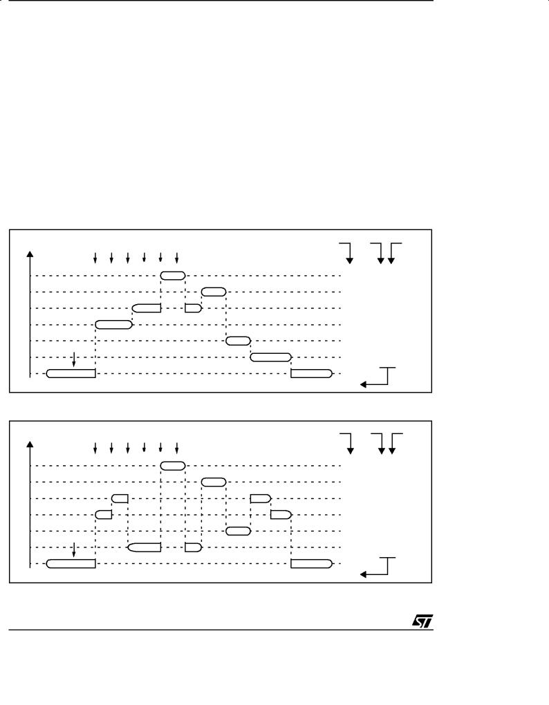
ST72311R, ST72511R, ST72512R, ST72532R
INTERRUPTS (Cont'd)
6.3 INTERRUPTS AND LOW POWER MODES
All interrupts allow the processor to exit the WAIT low power mode. On the contrary, only external and other specified interrupts allow the processor to exit the HALT modes (see column ªExit from HALTº in ªInterrupt Mappingº table). When several pending interrupts are present while exiting HALT mode, the first one serviced can only be an interrupt with exit from HALT mode capability and it is selected through the same decision process shown in Figure 15
Note: If an interrupt, that is not able to Exit from HALT mode, is pending with the highest priority when exiting HALT mode, this interrupt is serviced after the first one serviced.
Figure 16. Concurrent interrupt management
6.4 CONCURRENT & NESTED MANAGEMENT
The following Figure 16 and Figure 17 show two different interrupt management modes. The first is called concurrent mode and does not allow an interrupt to be interrupted, unlike the nested mode in Figure 17 The interrupt hardware priority is given in this order from the lowest to the highest: MAIN, IT4, IT3, IT2, IT1, IT0, TLI. The software priority is given for each interrupt.
Warning: A stack overflow may occur without notifying the software of the failure.
IT2 |
IT1 |
IT4 |
IT3 |
TLI |
IT0 |
PRIORITY |
|
TLI |
|
|
|
HARDWARE |
IT1 |
IT1 |
IT2 |
|
|
|
|
|
|
RIM |
|
|
MAIN |
|
|
11 / 10 |
|
Figure 17. Nested interrupt management
|
IT2 |
IT1 |
IT4 |
IT3 |
TLI |
IT0 |
PRIORITY |
|
|
|
|
|
TLI |
|
|
IT1 |
|
|
|
|
|
|
|
|
|
|
|
HARDWARE |
|
IT2 |
|
|
|
|
RIM |
|
|
|
|
|
|
|
|
|
IT4 |
|
IT4 |
|
MAIN |
|
|
|
|
|
|
|
|
|
|
|
|
|
|
11 / 10 |
|
|
|
|
|
SOFTWARE |
I1 |
|
|
I0 |
|
PRIORITY |
|
|
|||
|
|
|
|
||
LEVEL |
|
|
|
BYTES |
|
IT0 |
3 |
1 |
1 |
||
|
3 |
1 |
1 |
|
|
|
3 |
1 |
1 |
= 10 |
|
|
3 |
1 |
1 |
STACK |
|
|
|
||||
IT3 |
3 |
1 |
1 |
USED |
|
IT4 |
3 |
1 |
1 |
||
|
|||||
MAIN |
3/0 |
|
|
|
|
10 |
|
|
|
|
|
SOFTWARE |
I1 |
|
|
I0 |
|
PRIORITY |
|
|
|||
|
|
|
|
||
LEVEL |
|
|
|
BYTES |
|
IT0 |
3 |
1 |
1 |
||
|
3 |
1 |
1 |
|
|
IT1 |
2 |
0 |
0 |
= 20 |
|
IT2 |
1 |
0 |
1 |
STACK |
|
|
|||||
IT3 |
3 |
1 |
1 |
USED |
|
|
3 |
1 |
1 |
||
|
|
||||
MAIN |
3/0 |
|
|
|
|
10 |
|
|
|
|
30/164
 Loading...