


SGS Thomson Microelectronics ST92T163R4T1V, ST92T163R4T1L, ST92T163R4T1E, ST92T163R4T1, ST92T163N4B1E Datasheet
...ST92163
8/16-BIT FULL SPEED USB MCU FOR COMPOSITE DEVICES WITH 16 ENDPOINTS, 20K ROM, 2K RAM, I2C, SCI, & MFT
PRELIMINARY DATA
■Internal Memories: 20 Kbytes ROM/EPROM/ OTP, 2 Kbytes RAM
■Register oriented 8/16 bit core
■224 general purpose registers available as RAM, accumulators or index pointers
■Minimum instruction cycle time: 167 ns (@24 MHz CPU frequency)
■Low power modes: WFI, SLOW, HALT and STOP
■DMA controller for reduced processor overhead
■Full speed USB interface with DMA, compliant with USB specifications version 1.1 (in normal voltage mode)
■USB Embedded Functions with 16 fully configurable endpoints (buffer size programmable), supporting all USB data transfer types (Isochronous included)
■On-chip USB transceiver and 3.3 voltage regulator
■Multimaster I2C-bus serial interface up to 400KHz. with DMA capability
■Serial Communications Interface (SCI) with DMA capability:
±Asynchronous mode up to 315 Kb/s
±Synchronous mode up to 3 MHz
■External memory interface (8-bit data/16-bit address) with DMA capability from the USB
■16-bit Multi-Function Timer (12 operating modes) with DMA capability
■16-bit Timer with 8-bit prescaler and Watchdog
■6-channel, 8-bit A/D Converter (ADC)
■15 interrupt pins on 8 interrupt channels
■14 pins programmable as wake-up or additional external interrupts
■42 (DIP56) or 44 (QFP64) fully programmable I/Os with 6 or 8 high sink pads (10 mA @ 1 V)
■Programmable PLL clock generator (RCCU) using a low frequency external quartz (8 MHz)
■On-chip RC oscillator for low power operation
PSDIP56
TQFP64
■Low Voltage Detector Reset on some devices1
■Rich instruction set with 14 addressing modes
■Several operating voltage modes available on some devices1:
±Normal Voltage Mode
±8-MHz Low Voltage Mode
±16-MHz Low Voltage Mode
■0 - 24 MHz CPU clock operation @ 4.0-5.5 V (all devices)
■0 - 8 MHz CPU clock operation @ 3.0-4.0 V (8- MHz and 16-MHz Low Voltage devices)
■0 - 16 MHz CPU clock operation @ 3.0-4.0 V (16-MHz Low Voltage devices only)
■Division-by-zero trap generation
■0 oC to 70 oC temperature range
■Low EMI design supporting single sided PCB
■Complete development tools, including assembler, linker, C-compiler, archiver, source level debugger and hardware emulators, and Real Time Operating System
Note 1: Refer to ªDevice Summaryº on page 6 |
Rev. 1.9 |
|
|
January 2000 |
1/224 |
This is preliminary information on a new product in development orundergoing evaluation. Details are subject to change without notice.

Table of Contents
ST92163 . . . . . . . . . . . . . . . . . . . . . . . . . . . . . . . . . . . . . . . . . . . . 1
1 GENERAL DESCRIPTION . . . . . . . . . . . . . . . . . . . . . . . . . . . . . . . . . . . . . . . . . . . . . . . . . . . . . |
. 6 |
||
1.1 |
INTRODUCTION . . . . . . . . . . . . . . . . . . . . . . . . . . . . . . . . . . . . . . . . . . . . . . . . . . . . . . . . . |
6 |
|
|
1.1.1 |
Core Architecture . . . . . . . . . . . . . . . . . . . . . . . . . . . . . . . . . . . . . . . . . . . . . . . . . . . |
9 |
|
1.1.2 |
Instruction Set . . . . . . . . . . . . . . . . . . . . . . . . . . . . . . . . . . . . . . . . . . . . . . . . . . . . . . |
9 |
|
1.1.3 |
External MEMORY INTERFACE . . . . . . . . . . . . . . . . . . . . . . . . . . . . . . . . . . . . . . . |
9 |
|
1.1.4 |
OPERATING MODES . . . . . . . . . . . . . . . . . . . . . . . . . . . . . . . . . . . . . . . . . . . . . . . |
9 |
|
1.1.5 |
On-chip Peripherals . . . . . . . . . . . . . . . . . . . . . . . . . . . . . . . . . . . . . . . . . . . . . . . . |
10 |
1.2 |
PIN DESCRIPTION . . . . . . . . . . . . . . . . . . . . . . . . . . . . . . . . . . . . . . . . . . . . . . . . . . . . . . |
11 |
|
1.3 |
I/O PORT PINS . . . . . . . . . . . . . . . . . . . . . . . . . . . . . . . . . . . . . . . . . . . . . . . . . . . . . . . . . |
13 |
|
1.4 |
MEMORY MAP . . . . . . . . . . . . . . . . . . . . . . . . . . . . . . . . . . . . . . . . . . . . . . . . . . . . . . . . . |
19 |
|
1.5 |
ST92163 REGISTER MAP . . . . . . . . . . . . . . . . . . . . . . . . . . . . . . . . . . . . . . . . . . . . . . . . |
20 |
|
2 DEVICE ARCHITECTURE . . . . . . . . . . . . . . . . . . . . . . . . . . . . . . . . . . . . . . . . . . . . . . . . . . . . . |
27 |
||
2.1 |
CORE ARCHITECTURE . . . . . . . . . . . . . . . . . . . . . . . . . . . . . . . . . . . . . . . . . . . . . . . . . . |
27 |
|
2.2 |
MEMORY SPACES . . . . . . . . . . . . . . . . . . . . . . . . . . . . . . . . . . . . . . . . . . . . . . . . . . . . . . |
27 |
|
|
2.2.1 |
Register File . . . . . . . . . . . . . . . . . . . . . . . . . . . . . . . . . . . . . . . . . . . . . . . . . . . . . . |
27 |
|
2.2.2 |
Register Addressing . . . . . . . . . . . . . . . . . . . . . . . . . . . . . . . . . . . . . . . . . . . . . . . . |
29 |
2.3 |
SYSTEM REGISTERS . . . . . . . . . . . . . . . . . . . . . . . . . . . . . . . . . . . . . . . . . . . . . . . . . . . . |
30 |
|
|
2.3.1 |
Central Interrupt Control Register . . . . . . . . . . . . . . . . . . . . . . . . . . . . . . . . . . . . . . |
30 |
|
2.3.2 |
Flag Register . . . . . . . . . . . . . . . . . . . . . . . . . . . . . . . . . . . . . . . . . . . . . . . . . . . . . |
31 |
|
2.3.3 |
Register Pointing Techniques . . . . . . . . . . . . . . . . . . . . . . . . . . . . . . . . . . . . . . . . . |
32 |
|
2.3.4 |
Paged Registers . . . . . . . . . . . . . . . . . . . . . . . . . . . . . . . . . . . . . . . . . . . . . . . . . . . |
35 |
|
2.3.5 |
Mode Register . . . . . . . . . . . . . . . . . . . . . . . . . . . . . . . . . . . . . . . . . . . . . . . . . . . . |
35 |
|
2.3.6 |
Stack Pointers . . . . . . . . . . . . . . . . . . . . . . . . . . . . . . . . . . . . . . . . . . . . . . . . . . . . . |
36 |
2.4 |
MEMORY ORGANIZATION . . . . . . . . . . . . . . . . . . . . . . . . . . . . . . . . . . . . . . . . . . . . . . . . |
38 |
|
2.5 |
MEMORY MANAGEMENT UNIT . . . . . . . . . . . . . . . . . . . . . . . . . . . . . . . . . . . . . . . . . . . . |
39 |
|
2.6 |
ADDRESS SPACE EXTENSION . . . . . . . . . . . . . . . . . . . . . . . . . . . . . . . . . . . . . . . . . . . . |
40 |
|
|
2.6.1 |
Addressing 16-Kbyte Pages . . . . . . . . . . . . . . . . . . . . . . . . . . . . . . . . . . . . . . . . . . |
40 |
|
2.6.2 |
Addressing 64-Kbyte Segments . . . . . . . . . . . . . . . . . . . . . . . . . . . . . . . . . . . . . . . |
41 |
2.7 |
MMU REGISTERS . . . . . . . . . . . . . . . . . . . . . . . . . . . . . . . . . . . . . . . . . . . . . . . . . . . . . . . |
41 |
|
|
2.7.1 |
DPR[3:0]: Data Page Registers . . . . . . . . . . . . . . . . . . . . . . . . . . . . . . . . . . . . . . . |
41 |
|
2.7.2 |
CSR: Code Segment Register . . . . . . . . . . . . . . . . . . . . . . . . . . . . . . . . . . . . . . . . |
43 |
|
2.7.3 ISR: Interrupt Segment Register . . . . . . . . . . . . . . . . . . . . . . . . . . . . . . . . . . . . . . . |
43 |
|
|
2.7.4 DMASR: DMA Segment Register . . . . . . . . . . . . . . . . . . . . . . . . . . . . . . . . . . . . . . |
43 |
|
2.8 |
MMU USAGE . . . . . . . . . . . . . . . . . . . . . . . . . . . . . . . . . . . . . . . . . . . . . . . . . . . . . . . . . . . |
45 |
|
|
2.8.1 |
Normal Program Execution . . . . . . . . . . . . . . . . . . . . . . . . . . . . . . . . . . . . . . . . . . . |
45 |
|
2.8.2 |
Interrupts . . . . . . . . . . . . . . . . . . . . . . . . . . . . . . . . . . . . . . . . . . . . . . . . . . . . . . . . . |
45 |
|
2.8.3 |
DMA . . . . . . . . . . . . . . . . . . . . . . . . . . . . . . . . . . . . . . . . . . . . . . . . . . . . . . . . . . . . |
45 |
3 INTERRUPTS . . . . . . . . . . . . . . . . . . . . . . . . . . . . . . . . . . . . . . . . . . . . . . . . . . . . . . . . . . . . . . . |
46 |
||
3.1 |
INTRODUCTION . . . . . . . . . . . . . . . . . . . . . . . . . . . . . . . . . . . . . . . . . . . . . . . . . . . . . . . . |
46 |
|
3.2 |
INTERRUPT VECTORING . . . . . . . . . . . . . . . . . . . . . . . . . . . . . . . . . . . . . . . . . . . . . . . . |
47 |
|
|
3.2.1 Divide by Zero trap . . . . . . . . . . . . . . . . . . . . . . . . . . . . . . . . . . . . . . . . . . . . . . . . . |
47 |
|
|
3.2.2 Segment Paging During Interrupt Routines . . . . . . . . . . . . . . . . . . . . . . . . . . . . . . |
48 |
|
3.3 |
INTERRUPT PRIORITY LEVELS . . . . . . . . . . . . . . . . . . . . . . . . . . . . . . . . . . . . . . . . . . . |
48 |
|
2/224

Table of Contents
3.4 |
PRIORITY LEVEL ARBITRATION . . . . . . . . . . . . . . . . . . . . . . . . . . . . . . . . . . . . . . . . . . . |
48 |
|
|
3.4.1 Priority level 7 (Lowest) . . . . . . . . . . . . . . . . . . . . . . . . . . . . . . . . . . . . . . . . . . . . . |
48 |
|
|
3.4.2 Maximum depth of nesting . . . . . . . . . . . . . . . . . . . . . . . . . . . . . . . . . . . . . . . . . . . |
48 |
|
|
3.4.3 |
Simultaneous Interrupts . . . . . . . . . . . . . . . . . . . . . . . . . . . . . . . . . . . . . . . . . . . . . |
48 |
|
3.4.4 |
Dynamic Priority Level Modification . . . . . . . . . . . . . . . . . . . . . . . . . . . . . . . . . . . . |
49 |
3.5 |
ARBITRATION MODES . . . . . . . . . . . . . . . . . . . . . . . . . . . . . . . . . . . . . . . . . . . . . . . . . . . |
49 |
|
|
3.5.1 |
Concurrent Mode . . . . . . . . . . . . . . . . . . . . . . . . . . . . . . . . . . . . . . . . . . . . . . . . . . |
49 |
|
3.5.2 |
Nested Mode . . . . . . . . . . . . . . . . . . . . . . . . . . . . . . . . . . . . . . . . . . . . . . . . . . . . . |
52 |
3.6 |
EXTERNAL INTERRUPTS . . . . . . . . . . . . . . . . . . . . . . . . . . . . . . . . . . . . . . . . . . . . . . . . |
54 |
|
3.7 |
MANAGEMENT OF WAKE-UP LINES AND EXTERNAL INTERRUPT LINES . . . . . . . . . |
56 |
|
3.8 |
TOP LEVEL INTERRUPT . . . . . . . . . . . . . . . . . . . . . . . . . . . . . . . . . . . . . . . . . . . . . . . . . |
57 |
|
3.9 |
ON-CHIP PERIPHERAL INTERRUPTS . . . . . . . . . . . . . . . . . . . . . . . . . . . . . . . . . . . . . . |
57 |
|
3.10 INTERRUPT RESPONSE TIME . . . . . . . . . . . . . . . . . . . . . . . . . . . . . . . . . . . . . . . . . . . . |
58 |
||
3.11 INTERRUPT REGISTERS . . . . . . . . . . . . . . . . . . . . . . . . . . . . . . . . . . . . . . . . . . . . . . . . . 59
3.12 WAKE-UP / INTERRUPT LINES MANAGEMENT UNIT (WUIMU) . . . . . . . . . . . . . . . . . . 63
3.12.1 Introduction . . . . . . . . . . . . . . . . . . . . . . . . . . . . . . . . . . . . . . . . . . . . . . . . . . . . . . . 63
3.12.2 Main Features . . . . . . . . . . . . . . . . . . . . . . . . . . . . . . . . . . . . . . . . . . . . . . . . . . . . . 63
3.12.3 Functional Description . . . . . . . . . . . . . . . . . . . . . . . . . . . . . . . . . . . . . . . . . . . . . . 64
3.12.4 Programming Considerations . . . . . . . . . . . . . . . . . . . . . . . . . . . . . . . . . . . . . . . . . 66
3.12.5 Register Description . . . . . . . . . . . . . . . . . . . . . . . . . . . . . . . . . . . . . . . . . . . . . . . . 67
4 ON-CHIP DIRECT MEMORY ACCESS (DMA) . . . . . . . . . . . . . . . . . . . . . . . . . . . . . . . . . . . . . . 70
4.1 |
INTRODUCTION . . . . . . . . . . . . . . . . . . . . . . . . . . . . . . . . . . . . . . . . . . . . . . . . . . . . |
. . . . 70 |
|
4.2 |
DMA PRIORITY LEVELS . . . . . . . . . . . . . . . . . . . . . . . . . . . . . . . . . . . . . . . . . . . . . . |
. . . . 70 |
|
4.3 |
DMA TRANSACTIONS . . . . . . . . . . . . . . . . . . . . . . . . . . . . . . . . . . . . . . . . . . . . . . . |
. . . . 71 |
|
4.4 |
DMA CYCLE TIME . . . . . . . . . . . . . . . . . . . . . . . . . . . . . . . . . . . . . . . . . . . . . . . . . . . |
. . . . 73 |
|
4.5 |
SWAP MODE . . . . . . . . . . . . . . . . . . . . . . . . . . . . . . . . . . . . . . . . . . . . . . . . . . . . . . . |
. . . . 73 |
|
4.6 |
DMA REGISTERS . . . . . . . . . . . . . . . . . . . . . . . . . . . . . . . . . . . . . . . . . . . . . . . . . . . |
. . . . 74 |
|
5 RESET AND CLOCK CONTROL UNIT (RCCU) . . . . . . . . . . . . . . . . . . . . . . . . . . . . . . . . |
. . . . 75 |
||
5.1 |
INTRODUCTION . . . . . . . . . . . . . . . . . . . . . . . . . . . . . . . . . . . . . . . . . . . . . . . . . . . . |
. . . . 75 |
|
5.2 |
CLOCK CONTROL UNIT . . . . . . . . . . . . . . . . . . . . . . . . . . . . . . . . . . . . . . . . . . . . . . |
. . . . 75 |
|
|
5.2.1 |
Clock Control Unit Overview . . . . . . . . . . . . . . . . . . . . . . . . . . . . . . . . . . . . . . |
. . . . 75 |
5.3 |
CLOCK MANAGEMENT . . . . . . . . . . . . . . . . . . . . . . . . . . . . . . . . . . . . . . . . . . . . . . |
. . . . 77 |
|
|
5.3.1 |
PLL Clock Multiplier Programming . . . . . . . . . . . . . . . . . . . . . . . . . . . . . . . . . |
. . . . 78 |
|
5.3.2 |
CPU Clock Prescaling . . . . . . . . . . . . . . . . . . . . . . . . . . . . . . . . . . . . . . . . . . |
. . . . 78 |
|
5.3.3 |
Peripheral Clock . . . . . . . . . . . . . . . . . . . . . . . . . . . . . . . . . . . . . . . . . . . . . . . |
. . . . 78 |
|
5.3.4 |
Low Power Modes . . . . . . . . . . . . . . . . . . . . . . . . . . . . . . . . . . . . . . . . . . . . . |
. . . . 79 |
|
5.3.5 |
Interrupt Generation . . . . . . . . . . . . . . . . . . . . . . . . . . . . . . . . . . . . . . . . . . . . . |
. . . 79 |
5.4 |
CLOCK CONTROL REGISTERS . . . . . . . . . . . . . . . . . . . . . . . . . . . . . . . . . . . . . . . . . |
. . . 81 |
|
5.5 |
OSCILLATOR CHARACTERISTICS . . . . . . . . . . . . . . . . . . . . . . . . . . . . . . . . . . . . . . |
. . . 85 |
|
5.6 |
RESET/STOP MANAGER . . . . . . . . . . . . . . . . . . . . . . . . . . . . . . . . . . . . . . . . . . . . . . |
. . . 86 |
|
|
5.6.1 |
Reset Pin Timing . . . . . . . . . . . . . . . . . . . . . . . . . . . . . . . . . . . . . . . . . . . . . . . |
. . . 87 |
5.7 |
STOP MODE . . . . . . . . . . . . . . . . . . . . . . . . . . . . . . . . . . . . . . . . . . . . . . . . . . . . . . . . |
. . . 87 |
|
5.8 |
LOW VOLTAGE DETECTOR (LVD) RESET . . . . . . . . . . . . . . . . . . . . . . . . . . . . . . . . |
224. . . 88 |
|
3/224

Table of Contents
6 EXTERNAL MEMORY INTERFACE (EXTMI) . . . . . . . . . . . . . . . . . . . . . . . . . . . . . . . . . . . . . |
. 89 |
||
6.1 |
INTRODUCTION . . . . . . . . . . . . . . . . . . . . . . . . . . . . . . . . . . . . . . . . . . . . . . . . . . . . . . . |
. 89 |
|
6.2 |
EXTERNAL MEMORY SIGNALS . . . . . . . . . . . . . . . . . . . . . . . . . . . . . . . . . . . . . . . . . . . . |
90 |
|
|
6.2.1 |
AS: Address Strobe . . . . . . . . . . . . . . . . . . . . . . . . . . . . . . . . . . . . . . . . . . . . . . . . |
90 |
|
6.2.2 |
DS: Data Strobe . . . . . . . . . . . . . . . . . . . . . . . . . . . . . . . . . . . . . . . . . . . . . . . . . . . |
90 |
|
6.2.3 |
DS2: Data Strobe 2 . . . . . . . . . . . . . . . . . . . . . . . . . . . . . . . . . . . . . . . . . . . . . . . . . |
90 |
|
6.2.4 |
RW: Read/Write . . . . . . . . . . . . . . . . . . . . . . . . . . . . . . . . . . . . . . . . . . . . . . . . . . . |
93 |
|
6.2.5 BREQ, BACK: Bus Request, Bus Acknowledge . . . . . . . . . . . . . . . . . . . . . . . . . . . |
93 |
|
|
6.2.6 |
PORT 0 . . . . . . . . . . . . . . . . . . . . . . . . . . . . . . . . . . . . . . . . . . . . . . . . . . . . . . . . . . |
94 |
|
6.2.7 |
PORT 1 . . . . . . . . . . . . . . . . . . . . . . . . . . . . . . . . . . . . . . . . . . . . . . . . . . . . . . . . . . |
94 |
|
6.2.8 |
WAIT: External Memory Wait . . . . . . . . . . . . . . . . . . . . . . . . . . . . . . . . . . . . . . . . . |
94 |
6.3 |
REGISTER DESCRIPTION . . . . . . . . . . . . . . . . . . . . . . . . . . . . . . . . . . . . . . . . . . . . . . . . |
95 |
|
7 I/O PORTS . |
. . . . . . . . . . . . . . . . . . . . . . . . . . . . . . . . . . . . . . . . . . . . . . . . . . . . . . . . . . . . . . . . . |
98 |
|
7.1 |
INTRODUCTION . . . . . . . . . . . . . . . . . . . . . . . . . . . . . . . . . . . . . . . . . . . . . . . . . . . . . . . . |
98 |
|
7.2 |
SPECIFIC PORT CONFIGURATIONS . . . . . . . . . . . . . . . . . . . . . . . . . . . . . . . . . . . . . . . |
98 |
|
7.3 |
PORT CONTROL REGISTERS . . . . . . . . . . . . . . . . . . . . . . . . . . . . . . . . . . . . . . . . . . . . . |
98 |
|
7.4 |
INPUT/OUTPUT BIT CONFIGURATION . . . . . . . . . . . . . . . . . . . . . . . . . . . . . . . . . . . . . . |
99 |
|
7.5 |
ALTERNATE FUNCTION ARCHITECTURE . . . . . . . . . . . . . . . . . . . . . . . . . . . . . . . . . . |
103 |
|
|
7.5.1 Pin Declared as I/O . . . . . . . . . . . . . . . . . . . . . . . . . . . . . . . . . . . . . . . . . . . . . . . . |
103 |
|
|
7.5.2 Pin Declared as an Alternate Input . . . . . . . . . . . . . . . . . . . . . . . . . . . . . . . . . . . . |
103 |
|
|
7.5.3 Pin Declared as an Alternate Function Output . . . . . . . . . . . . . . . . . . . . . . . . . . . |
103 |
|
7.6 |
I/O STATUS AFTER WFI, HALT AND RESET . . . . . . . . . . . . . . . . . . . . . . . . . . . . . . . . |
103 |
|
8 ON-CHIP PERIPHERALS . . . . . . . . . . . . . . . . . . . . . . . . . . . . . . . . . . . . . . . . . . . . . . . . . . . . . |
104 |
||
8.1 |
TIMER/WATCHDOG (WDT) . . . . . . . . . . . . . . . . . . . . . . . . . . . . . . . . . . . . . . . . . . . . . . |
104 |
|
|
8.1.1 |
Introduction . . . . . . . . . . . . . . . . . . . . . . . . . . . . . . . . . . . . . . . . . . . . . . . . . . . . . . |
104 |
|
8.1.2 |
Functional Description . . . . . . . . . . . . . . . . . . . . . . . . . . . . . . . . . . . . . . . . . . . . . |
105 |
|
8.1.3 |
Watchdog Timer Operation . . . . . . . . . . . . . . . . . . . . . . . . . . . . . . . . . . . . . . . . . . |
106 |
|
8.1.4 |
WDT Interrupts . . . . . . . . . . . . . . . . . . . . . . . . . . . . . . . . . . . . . . . . . . . . . . . . . . . |
108 |
|
8.1.5 |
Register Description . . . . . . . . . . . . . . . . . . . . . . . . . . . . . . . . . . . . . . . . . . . . . . . |
109 |
8.2 |
MULTIFUNCTION TIMER (MFT) . . . . . . . . . . . . . . . . . . . . . . . . . . . . . . . . . . . . . . . . . . . |
111 |
|
|
8.2.1 |
Introduction . . . . . . . . . . . . . . . . . . . . . . . . . . . . . . . . . . . . . . . . . . . . . . . . . . . . . . |
111 |
|
8.2.2 |
Functional Description . . . . . . . . . . . . . . . . . . . . . . . . . . . . . . . . . . . . . . . . . . . . . |
113 |
|
8.2.3 |
Input Pin Assignment . . . . . . . . . . . . . . . . . . . . . . . . . . . . . . . . . . . . . . . . . . . . . . |
116 |
|
8.2.4 |
Output Pin Assignment . . . . . . . . . . . . . . . . . . . . . . . . . . . . . . . . . . . . . . . . . . . . . |
120 |
|
8.2.5 |
Interrupt and DMA . . . . . . . . . . . . . . . . . . . . . . . . . . . . . . . . . . . . . . . . . . . . . . . . |
122 |
|
8.2.6 |
Register Description . . . . . . . . . . . . . . . . . . . . . . . . . . . . . . . . . . . . . . . . . . . . . . . |
124 |
8.3 |
USB PERIPHERAL (USB) . . . . . . . . . . . . . . . . . . . . . . . . . . . . . . . . . . . . . . . . . . . . . . . . |
135 |
|
|
8.3.1 |
Introduction . . . . . . . . . . . . . . . . . . . . . . . . . . . . . . . . . . . . . . . . . . . . . . . . . . . . . . |
135 |
|
8.3.2 |
Main Features . . . . . . . . . . . . . . . . . . . . . . . . . . . . . . . . . . . . . . . . . . . . . . . . . . . . |
135 |
|
8.3.3 |
Functional Description . . . . . . . . . . . . . . . . . . . . . . . . . . . . . . . . . . . . . . . . . . . . . |
135 |
|
8.3.4 |
Register Description . . . . . . . . . . . . . . . . . . . . . . . . . . . . . . . . . . . . . . . . . . . . . . . |
138 |
|
8.3.5 |
Register pages summary . . . . . . . . . . . . . . . . . . . . . . . . . . . . . . . . . . . . . . . . . . . |
148 |
8.4 |
SERIAL COMMUNICATIONS INTERFACE (SCI) . . . . . . . . . . . . . . . . . . . . . . . . . . . . . . |
150 |
|
8.4.1 Introduction . . . . . . . . . . . . . . . . . . . . . . . . . . . . . . . . . . . . . . . . . . . . . . . . . . . . . . 150
8.4.2 Functional Description . . . . . . . . . . . . . . . . . . . . . . . . . . . . . . . . . . . . . . . . . . . . . 151
8.4.3 SCI Operating Modes . . . . . . . . . . . . . . . . . . . . . . . . . . . . . . . . . . . . . . . . . . . . . . 152
4/224

Table of Contents
|
8.4.4 |
Serial Frame Format . . . . . . . . . . . . . . . . . . . . . . . . . . . . . . . . . . . . . . . . . . . . . . . |
155 |
|
8.4.5 |
Clocks And Serial Transmission Rates . . . . . . . . . . . . . . . . . . . . . . . . . . . . . . . . . |
158 |
|
8.4.6 |
SCI Initialization Procedure . . . . . . . . . . . . . . . . . . . . . . . . . . . . . . . . . . . . . . . . . |
158 |
|
8.4.7 |
Input Signals . . . . . . . . . . . . . . . . . . . . . . . . . . . . . . . . . . . . . . . . . . . . . . . . . . . . . |
160 |
|
8.4.8 |
Output Signals . . . . . . . . . . . . . . . . . . . . . . . . . . . . . . . . . . . . . . . . . . . . . . . . . . . |
160 |
|
8.4.9 |
Interrupts and DMA . . . . . . . . . . . . . . . . . . . . . . . . . . . . . . . . . . . . . . . . . . . . . . . . |
161 |
|
8.4.10 Register Description . . . . . . . . . . . . . . . . . . . . . . . . . . . . . . . . . . . . . . . . . . . . . . . |
164 |
|
8.5 |
I2C BUS INTERFACE . . . . . . . . . . . . . . . . . . . . . . . . . . . . . . . . . . . . . . . . . . . . . . . . . . . |
175 |
|
|
8.5.1 |
Introduction . . . . . . . . . . . . . . . . . . . . . . . . . . . . . . . . . . . . . . . . . . . . . . . . . . . . . . |
175 |
|
8.5.2 |
Main Features . . . . . . . . . . . . . . . . . . . . . . . . . . . . . . . . . . . . . . . . . . . . . . . . . . . . |
175 |
|
8.5.3 |
Functional Description . . . . . . . . . . . . . . . . . . . . . . . . . . . . . . . . . . . . . . . . . . . . . |
176 |
|
8.5.4 |
I2C State Machine . . . . . . . . . . . . . . . . . . . . . . . . . . . . . . . . . . . . . . . . . . . . . . . . |
178 |
|
8.5.5 |
Interrupt Features . . . . . . . . . . . . . . . . . . . . . . . . . . . . . . . . . . . . . . . . . . . . . . . . . |
183 |
|
8.5.6 |
DMA Features . . . . . . . . . . . . . . . . . . . . . . . . . . . . . . . . . . . . . . . . . . . . . . . . . . . . |
184 |
|
8.5.7 |
Register Description . . . . . . . . . . . . . . . . . . . . . . . . . . . . . . . . . . . . . . . . . . . . . . . |
186 |
8.6 |
A/D CONVERTER (A/D) . . . . . . . . . . . . . . . . . . . . . . . . . . . . . . . . . . . . . . . . . . . . . . . . . |
197 |
|
8.6.1 Introduction . . . . . . . . . . . . . . . . . . . . . . . . . . . . . . . . . . . . . . . . . . . . . . . . . . . . . . 197 8.6.2 Main Features . . . . . . . . . . . . . . . . . . . . . . . . . . . . . . . . . . . . . . . . . . . . . . . . . . . . 197 8.6.3 General Description . . . . . . . . . . . . . . . . . . . . . . . . . . . . . . . . . . . . . . . . . . . . . . . 197 8.6.4 Register Description . . . . . . . . . . . . . . . . . . . . . . . . . . . . . . . . . . . . . . . . . . . . . . . 199
9 ELECTRICAL CHARACTERISTICS . . . . . . . . . . . . . . . . . . . . . . . . . . . . . . . . . . . . . . . . . . . . . 201 10 GENERAL INFORMATION . . . . . . . . . . . . . . . . . . . . . . . . . . . . . . . . . . . . . . . . . . . . . . . . . . . 218
10.1 EPROM/OTP PROGRAMMING . . . . . . . . . . . . . . . . . . . . . . . . . . . . . . . . . . . . . . . . . . . . 218 10.2 PACKAGE DESCRIPTION . . . . . . . . . . . . . . . . . . . . . . . . . . . . . . . . . . . . . . . . . . . . . . . 219 10.3 ORDERING INFORMATION . . . . . . . . . . . . . . . . . . . . . . . . . . . . . . . . . . . . . . . . . . . . . . 221 10.4 TRANSFER OF CUSTOMER CODE . . . . . . . . . . . . . . . . . . . . . . . . . . . . . . . . . . . . . . . . 221
224
5/224
ST92163 - GENERAL DESCRIPTION
1 GENERAL DESCRIPTION
1.1 INTRODUCTION
The ST9216x family brings the enhanced ST9 reg- ister-based architecture to a new range of highperformance microcontrollers specifically designed for USB (Universal Serial Bus) applications. Their performance derives from the use of a flexible 256-register programming model for ultrafast context switching and real-time event response. The intelligent on-chip peripherals offload the ST9 core from I/O and data management processing tasks allowing critical application tasks to get the maximum use of core resources. The ST9 MCU devices support low power consumption and low voltage operation for power-efficient and low-cost embedded systems. In the ST92163 family, four different types of device are available:
Normal Voltage Devices with LVD function
They operate in Normal Voltage Mode only (4.0- 5.5V @ 24MHz) and include the Low Voltage Detector (LVD) function.
Normal Voltage Devices without LVD function
They operate in Normal Voltage Mode only (4.0- 5.5V @ 24MHz) and do not include the Low Voltage Detector (LVD) function.
Device Summary
8-MHz Low Voltage Devices
They do not include the Low Voltage Detector (LVD) function and they support two operating voltage modes:
±Normal Voltage mode (4.0-5.5V @ 24MHz) with full functionality including USB.
±8-MHz Low Voltage mode (3.0-4.0V @ 8MHz) without the USB interface.
16-MHz Low Voltage Devices
They do not include the Low Voltage Detector (LVD) function and they support three operating voltage modes:
±Normal Voltage mode (4.0-5.5V @ 24MHz) with full functionality including USB.
±8-MHz Low Voltage mode (3.0-4.0V @ 8MHz) without the USB interface.
±16-MHz Low Voltage mode (3.0-4.0V @ 16MHz) without the USB interface.
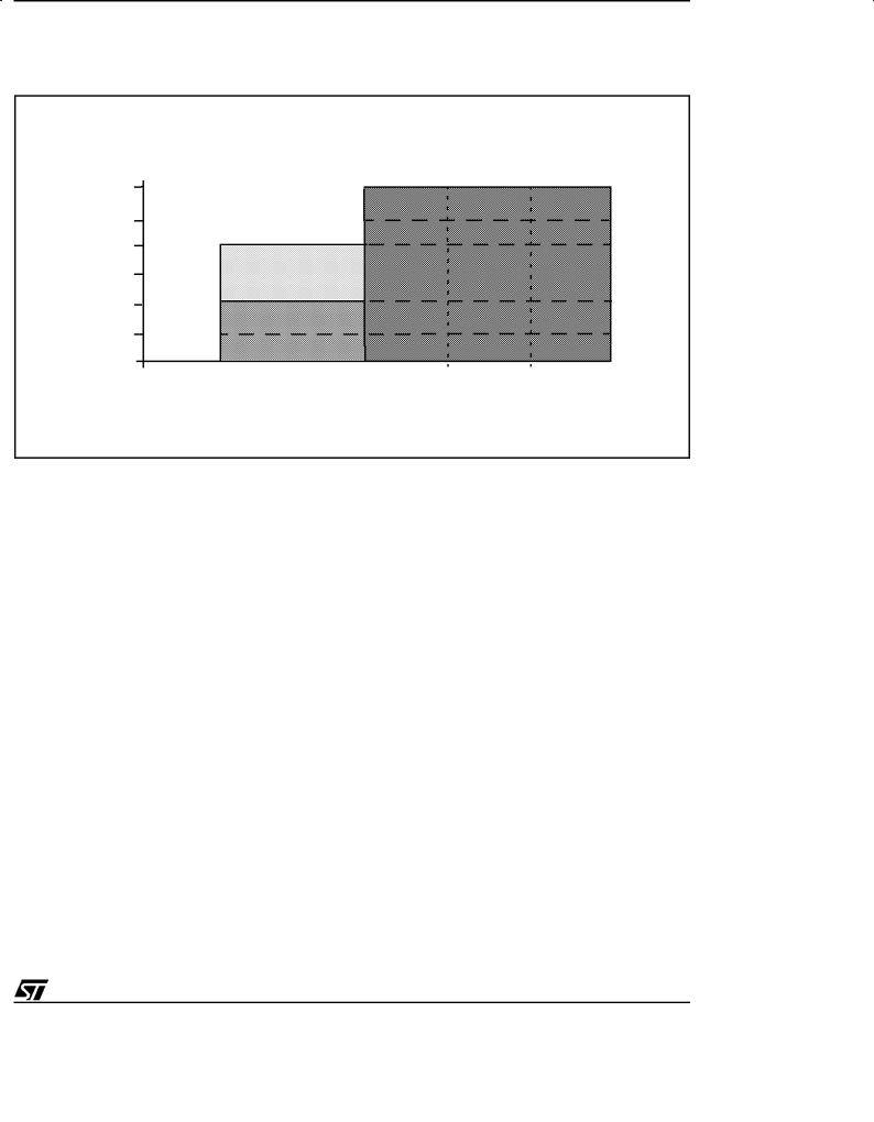
Figure 1, on page 7 shows the operating range of the ST92163 devices.
16-MHz 8-MHz
Device |
Package |
Program Memory |
RAM Low Voltage Low Voltage LVD |
USB |
|
ST921631 |
|
|
Mode |
Mode |
|
PSDIP56/ |
20K ROM |
|
|
|
|
ST92T163 |
TQFP64 |
20K OTP |
|
Yes |
|
|
CSDIP56/ |
|
|
|
|
ST92E163 |
20K EPROM |
|
|
|
|
CQFP64 |
|
|
Yes |
||
|
|
|
No |
||
ST92163E1 |
PSDIP56/ |
20K ROM |
|
|
|
No |
|
|
|||
ST92T163E |
TQFP64 |
20K OTP |
|
|
|
ST92E163E |
CSDIP56/ |
20K EPROM |
2K |
|
|
CQFP64 |
|
|
|
||
ST92163L1 |
|
|
|
|
|
TQFP64 |
20K ROM |
|
No |
|
|
ST92T163L |
20K OTP |
|
|
||
|
|
|
|
||
ST92E163L |
CQFP64 |
20K EPROM |
|
Yes |
In Normal |
ST92163V1 |
|
20K ROM |
|
Mode only |
|
TQFP64 |
|
|
|||
ST92T163V1 |
20K OTP |
Yes |
|
|
|
|
|
|
|||
ST92E163V1 |
CQFP64 |
20K EPROM |
|
|
|
1 Contact sales office for availability
6/224
ST92163 - GENERAL DESCRIPTION
INTRODUCTION (Cont'd)
Figure 1. Maximum Operating Frequency (fMAX) versus Supply Voltage (VDD)
MAX FREQUE NCY (MHz)
24 |
|
|
20 |
NOT |
GUARANTEED AREATHISIN |
16 |
FUNCTIONALITYIS |
|
|
|
|
12 |
|
|
8
4
0
2.5
|
16-MHz LOW VOLTAGE |
NORMAL VOLTAGE MODE 3) |
|
|
|
MODE 1) |
|
|
|
|
8-MHz LOW VOLTAGE |
|
|
|
|
MODE 2) |
|
|
|
3.0 |
4 |
4.5 |
5 |
5.5 |
SUPPLY VOLTAGE (V)
Notes:
1)This mode is supported by 16-MHz Low Voltage devices only
2)This mode is supported by 8-MHz Low Voltage devices and 16-MHz Low Voltage devices
3)This mode is supported by all devices
7/224

ST92163 - GENERAL DESCRIPTION
INTRODUCTION (Cont'd)
Figure 2. ST92163 Architectural Block Diagram
USBGND USBVCC USBDM0 USBDP0
USBOE USBSOF
INT[7:0]
NMI
WKUP[14:0]
OSCIN OSCOUT RESET
INTCLK
WDIN
WDOUT
20K ROM/ EPROM/OTP
2K RAM
DMA
USB with 16 end-
points
9V/3.3V Voltage Regulator
256 bytes Register File
8/16-bit CPU
Interrupt
Management
DMA
ST9+ CORE
Wakeup
and Interrupt
Management
RCCU
WATCHDOG
TIMER
MEMORY BUS
External
Memory
Interface
MF TIMER
A/D Converter
Fully Prog.
I/Os
Low Voltage
Detector
LVD**
SCI
REGISTER BUS
I2C BUS
MIRROR
REGISTER
All alternate functions (Italic characters) are mapped on Ports 0,1, 3, 4, 5 and 6
*64-pin devices only
**on some devices only (refer to ªDevice Summaryº on page 6)
AS
BACK
BREQ
DS
WAIT
RW
A[15:0]
D[7:0]
TINA
TINB
TOUTA
TOUTB
AIN[5:0] EXTRG
P0[7:0]
P1[7:0]
P3[7:0]
P4[3:0]
P5[7:0]
P6[5:0] P6[7:6]*
TXCLK RXCLK SIN DCD SOUT CLKOUT RTS SDS
SDA
SCL
8/224

INTRODUCTION (Cont'd)
1.1.1 Core Architecture
The nucleus of the ST92163 is the enhanced ST9 Core that includes the Central Processing Unit (CPU), the register file, the interrupt and DMA controller, and the Memory Management Unit (MMU).
Three independent buses are controlled by the Core: a 22-bit memory bus, an 8-bit register addressing bus and a 6-bit interrupt/DMA bus which connects the interrupt and DMA controllers in the on-chip peripherals with the core.
This multiple bus architecture makes the ST9 family devices highly efficient for accessing on and off-chip memory and fast exchange of data with the on-chip peripherals.
The general-purpose registers can be used as accumulators, index registers, or address pointers. Adjacent register pairs make up 16-bit registers for addressing or 16-bit processing. Although the ST9 has an 8-bit ALU, the chip handles 16-bit operations, including arithmetic, loads/stores, and memory/register and memory/memory exchanges. Many opcodes specify byte or word operations, the hardware automatically handles 16-bit operations and accesses.
For interrupts or subroutine calls, the CPU uses a system stack in conjunction with the stack pointer (SP). A separate user stack has its own SP. The separate stacks, without size limitations, can be in on-chip RAM (or in Register File) or off-chip memory.
1.1.2 Instruction Set
The ST9 instruction set consists of 94 instruction types, including instructions for bit handling, byte (8-bit) and word (16-bit) data, as well as BCD and Boolean formats. Instructions have been added to facilitate large program and data handling through the MMU, as well as to improve the performance and code density of C Function calls. 14 addressing modes are available, including powerful indirect addressing capabilities.
The bit-manipulation instructions of the ST9 are set, clear, complement, test and set, load, and various logic instructions (AND, OR, and XOR). Math
ST92163 - GENERAL DESCRIPTION
functions include add, subtract, increment, decrement, decimal adjust, multiply and divide.
1.1.3 External MEMORY INTERFACE
The ST92163 device has a 16-bit external address bus allowing it to address up to 64K bytes of external memory.
1.1.4 OPERATING MODES
To optimize performance versus the power consumption of the device, ST9 devices now support a range of operating modes that can be dynamically selected depending on the performance and functionality requirements of the application at a given moment.
Run Mode. This is the full speed execution mode with CPU and peripherals running at the maximum clock speed delivered by the Phase Locked Loop (PLL) of the Clock Control Unit (CCU).
Slow Mode. Power consumption can be significantly reduced by running the CPU and the peripherals at reduced clock speed using the CPU Prescaler and CCU Clock Divider.
Wait For Interrupt Mode. The Wait For Interrupt (WFI) instruction suspends program execution until an interrupt request is acknowledged. During WFI, the CPU clock is halted while the peripheral and interrupt controller keep running at a frequency programmable via the CCU. In this mode, the power consumption of the device can be reduced by more than 95% (LP WFI).
Halt Mode. When executing the HALT instruction, and if the Watchdog is not enabled, the CPU and its peripherals stop operating and the status of the machine remains frozen (the clock is also stopped). A reset is necessary to exit from Halt mode.
Stop Mode. Under user program control, (see Wake-up and Interrupt Management Unit), the CPU and its peripherals stop operating and the status of the machine remains frozen (the clock is also stopped) until program execution is woken up by an event on an external Wake-up pin.
9/224

ST92163 - GENERAL DESCRIPTION
INTRODUCTION (Cont'd)
1.1.5 On-chip Peripherals
USB Interface
The USB interface provides a full speed USB 1.1 compliant port with embedded transceiver and voltage regulator. Up to 16 endpoints are available supporting up to 8 USB devices. Separate transmit and receive DMA channels are available for each device for fast data transfers with internal RAM.
Parallel I/O Ports
The ST9 is provided with dedicated lines for input/ output. These lines, grouped into 8-bit ports, can be independently programmed to provide parallel input/output or to carry input/output signals to or from the on-chip peripherals and core. All ports have active pull-ups and pull-down resistors compatible with TTL loads. In addition pull-ups can be turned off for open drain operation and weak pullups can be turned on to save chip resistive pullups. Input buffers can be either TTL or CMOS compatible.
High Current (10 mA) outputs are available for driving external devices such as LEDs.
Multifunction Timer
The Multifunction Timer has a 16-bit Up/Down counter supported by two 16-bit compare registers, two 16-bit input capture registers and two DMA channels. Timing resolution can be programmed using an 8-bit prescaler. 12 operating modes allow a range of different timing functions to be easily performed such as complex waveform generatation, measurement or PWM output.
16-bit Timer/Watchdog
The Timer/Watchdog peripheral can be used as a watchdog or for a wide range of other timing functions such as generating periodic interrupts, measuring input signal pulse widths, requesting an interrupt after a set number of events. It can also generate a square wave or PWM output signal.
Serial Communications Controller
The SCI provides a synchronous or asynchronous serial I/O port using two DMA channels. Baud rates and data formats are programmable. Controller applications can further benefit from the self test and address wake-up facility offered by the character search mode.
I2C Bus Interface
The I2C bus is a synchronous serial bus for connecting multiple devices using a data line and a clock line. Multimaster and slave modes are supported. Data transfer between the bus and memory is performed by DMA. The I2C interface supports 7 and 10-bit addressing. It operates in multimaster or slave mode and supports speeds of up to 400 KHz. Bus events (Bus busy, slave address recognized) and error conditions are automatically flagged in peripheral registers and interrupts are optionally generated.
Analog/Digital Converter
The ADC provides up to 6 analog inputs with onchip sample and hold, fast conversion time and 8- bit resolution. Conversion can be triggered by a signal from the Multifunction Timer (MFT).
10/224
ST92163 - GENERAL DESCRIPTION
1.2 PIN DESCRIPTION
Figure 3. 64-Pin Package Pin-Out
P1.3/A11/WKUP14 64
WKUP14/A10/P1.2 1 WKUP14/A9/P1.1 WKUP14/A8/P1.0
D7/A7/P0.7
D6/A6/P0.6
D5/A5/P0.5
D4/A4/P0.4
D3/A3/P0.3
D2/A2/P0.2
D1/A1/P0.1
D0/A0/P0.0
AIN5/P6.7
AIN4/P6.6
USBSOF/AIN3/P6.5
USBSOF/AIN2/P6.4 WKUP13/AIN1/P6.3 16
AVDD
P1.4/A12/WKUP14 P1.5/A13/WKUP14 |
P1.6/A14/WKUP14 P1.7/A15/WKUP14 N.C. N.C. |
V |
V P4.0/BREQ P4.1/WAIT P4.2 |
P4.3//BACK USBDM0 |
USBDP0 N.C. |
|
|
SS |
DD |
|
|
|
|
|
|
|
48 |
|
|
|
|
|
|
|
|
|
|
|
|
|
|
32 |
WKUP12/AIN0/INTCLK/P6.2 |
WKUP11/SCL/EXTRG/INT6/P6.1 |
WKUP10/SDA/INT5/P6.0 |
DD |
OSCIN |
SS |
OSCOUT |
WDOUT/NMI/P5.7 |
WKUP9/TOUTB/P5.6 |
RW/WDIN/INT0/P5.5 |
USBOE/WKUP8/P5.4 |
TOUTA/INT2/P5.3 |
INT3/P5.2 |
TINB/INT4/P5.1 |
N.C. |
V |
V |
N.C. USBVCC USBGND DS
P3.0/INT7/SOUT
P3.1/INT7/RTS
P3.2/INT7/TXCLK/CLKOUT
P3.3/INT7/RXCLK
P3.4/INT7/DCD
P3.5/INT7/SIN
P3.6/INT7/AS
P3.7/INT7/SDS
VPP
RESET P5.0/INT1/TINA N.C.
N.C. = Not connected
11/224

ST92163 - GENERAL DESCRIPTION
Figure 4. 56-Pin Package Pin-Out
WKUP3/RXCLK/INT7/P3.3 |
1 |
56 |
P3.4/INT7/DCD/WKUP4 |
WKUP2/CLKOUT/TXCLK/INT7/P3.2 |
|
|
P3.5/INT7/SIN/WKUP5 |
WKUP1/RTS/INT7/P3.1 |
|
|
P3.6/INT7/ASN/WKUP6 |
WKUP0/SOUT/INT7/P3.0 |
|
|
P3.7/INT7/SDS/WKUP7 |
DS |
|
|
VPP |
USBGND |
|
|
RESET |
USBVCC |
|
|
P5.0/INT1/TI NA |
USBDP0 |
|
|
P5.1/INT4/TI NB |
USBDM0 |
|
|
P5.2/INT3 |
BACK/P4.3 |
|
|
P5.3/INT2/TO UTA |
P4.2 |
|
|
P5.4/WKUP8/USBOE |
WAIT/P4.1 |
|
|
P5.5/INT0/WDIN/RW |
BREQ/P4.0 |
|
|
P5.6/TOUTB/WKUP9 |
VDD |
|
|
P5.7/NMI/WDOUT |
VSS |
|
|
OSCOUT |
WKUP14/A15/P1.7 |
|
|
VSS |
WKUP14/A14/P1.6 |
|
|
OSCIN |
WKUP14/A13/P1.5 |
|
|
VDD |
WKUP14/A12/P1.4 |
|
|
P6.0/INT5/SDA/WKUP10 |
WKUP14/A11/P1.3 |
|
|
P6.1/INT6/EXTRG/SCL/WKUP11 |
WKUP14/A10/P1.2 |
|
|
P6.2/INTCLK/AIN0/WKUP12 |
WKUP14/A9/P1.1 |
|
|
AVDD |
WKUP14/A8/P1.0 |
|
|
P6.3/AIN1/WKUP13 |
D7/A7/P0.7 |
|
|
P6.4/AIN2/USBSOF |
D6/A6/P0.6 |
|
|
P6.5/AIN3/USBSOF |
D5/A5/P0.5 |
|
|
P0.0/A0/D0 |
D4/A4/P0.4 |
28 |
29 |
P0.1/A1/D1 |
D3/A3/P0.3 |
P0.2/A2/D2 |
Table 1. Power Supply Pins
Name |
Function |
|
VDD |
Main Power Supply Voltage |
|
(2 pins internally connected) |
||
|
||
VSS |
Digital Circuit Ground |
|
(2 pins internally connected) |
||
|
||
AVDD |
Analog Circuit Supply Voltage |
|
VPP |
EPROM Programming Voltage. |
|
Must be connected to ground in |
||
|
normal operating mode. |
DIP56 |
QFP64 |
1421
3956
1523
4157
3517
52 36
Table 2. Primary Function pins
Name |
Function |
DS |
Data Strobe |
OSCIN |
Oscillator Input |
OSCOUT |
Oscillator Output |
RESET |
Reset to initialize the ST9 |
USBGND |
USB bus ground level |
USBVCC |
USB voltage regulator output |
USBDM0 |
USB Upstream port Dataline |
USBDP0 |
USB Upstream port Data+ line |
DIP56 |
QFP64 |
5 |
45 |
40 |
22 |
42 |
24 |
51 |
35 |
646
747
9 |
51 |
8 |
50 |
12/224

ST92163 - GENERAL DESCRIPTION
1.3 I/O Port Pins
All the ports of the device can be programmed as Input/Output or in Input mode, compatible with TTL or CMOS levels (except where Schmitt Trigger is present). Each bit can be programmed individually (Refer to the I/O ports chapter).
TTL/CMOS Input
For all those port bits where no input schmitt trigger is implemented, it is always possible to program the input level as TTL or CMOS compatible by programming the relevant PxC2.n control bit.
Refer I/O Ports Chapter to the section titled ªInput/ Output Bit Configurationº.
Table 3. I/O Port Characteristics
Push-Pull/OD Output
The output buffer can be programmed as pushpull or open-drain: attention must be paid to the fact that the open-drain option corresponds only to a disabling of P-channel MOS transistor of the buffer itself: it is still present and physically connected to the pin. Consequently it is not possible to increase the output voltage on the pin over VDD+0.3 Volt, to avoid direct junction biasing.
Pure Open-drain Output
The user can increase the voltage on an I/O pin over VDD+0.3 Volt where the P-channel MOS transistor is physically absent: this is allowed on all ªPure Open Drainº pins. Of course, in this case the push-pull option is not available and any weak pull-up must implemented externally.
|
Input |
Output |
Weak Pull-Up |
Reset State |
Port 0[7:0] |
TTL/CMOS |
Push-Pull/OD |
Yes |
Bidirectional WPU |
Port 1[7:0] |
TTL/CMOS |
Push-Pull/OD |
Yes |
Bidirectional WPU |
Port 3[7:0] |
Schmitt trigger |
Push-Pull/OD |
Yes |
Bidirectional WPU |
Port 4[3:0] |
Schmitt trigger |
Push-Pull/OD |
Yes |
Bidirectional WPU |
Port 5[7:0] |
Schmitt trigger |
Push-Pull/OD |
Yes |
Bidirectional WPU |
Port 6[1:0] |
Schmitt trigger |
Pure Open Drain with high sink capability |
No |
Bidirectional |
Port 6[5:2] |
TTL/CMOS |
Push-Pull/OD with high sink capability |
Yes |
Bidirectional WPU |
Port 6.6 |
Schmitt trigger |
Push-Pull/OD with high sink capability |
No |
Bidirectional |
Port 6.7 |
TTL/CMOS |
Push-Pull/OD with high sink capability |
No |
Bidirectional |
Legend: WPU = Weak Pull-Up, OD = Open Drain
13/224

ST92163 - GENERAL DESCRIPTION
Table 4. ST92163 Alternate Functions
Port General
Name Purpose I/O
P0.0
P0.1
P0.2
P0.3
P0.4
P0.5
P0.6
P0.7
P1.0
P1.1
P1.2
All ports useable for general pur-
P1.3 pose I/O (input, output or bidirectional)
P1.4
P1.5
P1.6
P1.7
P3.0
P3.1
Pin
No.
DIP56 |
QFP64 |
|
|
31 |
11 |
A0/D0 |
|
30 |
10 |
A1/D1 |
|
29 |
9 |
A2/D2 |
|
28 |
8 |
A3/D3 |
|
27 |
7 |
A4/D4 |
|
26 |
6 |
A5/D5 |
|
25 |
5 |
A6/D6 |
|
24 |
4 |
A7/D7 |
|
23 |
3 |
A8 |
|
WKUP14 |
|||
|
|
||
22 |
2 |
A9 |
|
WKUP14 |
|||
|
|
||
21 |
1 |
A10 |
|
WKUP14 |
|||
|
|
||
20 |
64 |
A11 |
|
WKUP14 |
|||
|
|
||
19 |
63 |
A12 |
|
WKUP14 |
|||
|
|
||
18 |
62 |
A13 |
|
WKUP14 |
|||
|
|
||
17 |
61 |
A14 |
|
WKUP14 |
|||
|
|
||
16 |
60 |
A15 |
|
WKUP14 |
|||
|
|
WKUP0
444 INT7 SOUT WKUP1
3 43 INT7 RTS
|
Alternate Functions |
I/O |
Ext. Mem. Address/Data bit 0 |
I/O |
Ext. Mem. Address/Data bit 1 |
I/O |
Ext. Mem. Address/Data bit 2 |
I/O |
Ext. Mem. Address/Data bit 3 |
I/O |
Ext. Mem. Address/Data bit 4 |
I/O |
Ext. Mem. Address/Data bit 5 |
I/O |
Ext. Mem. Address/Data bit 6 |
I/O |
Ext. Mem. Address/Data bit 7 |
I/O |
Ext. Mem. Address bit 8 |
I |
Wakeup Line 14 (***) |
I/O |
Ext. Mem. Address bit 9 |
I |
Wakeup Line 14 (***) |
I/O |
Ext. Mem. Address bit 10 |
I |
Wakeup Line 14 (***) |
I/O |
Ext. Mem. Address bit 11 |
I |
Wakeup Line 14 (***) |
I/O |
Ext. Mem. Address bit 12 |
I |
Wakeup Line 14 (***) |
I/O |
Ext. Mem. Address bit 13 |
I |
Wakeup Line 14 (***) |
I/O |
Ext. Mem. Address bit 14 |
I |
Wakeup Line 14 (***) |
I/O |
Ext. Mem. Address bit 15 |
I |
Wakeup Line 14 (***) |
I |
Wakeup Line 0 |
I |
External Interrupt 7 (*) |
O |
SCI Data Output |
O |
Wakeup Line 1 |
I |
External Interrupt 7 (*) |
O |
SCI Request to Send |
14/224
ST92163 - GENERAL DESCRIPTION
Port General
Name Purpose I/O
Pin
No.
DIP56 |
QFP64 |
Alternate Functions
P3.2
P3.3
P3.4
P3.5
P3.6
P3.7
P4.0
P4.1
P4.2
P4.3
All ports useable
for general purpose I/O (input,
output or bidirec-
tional)
|
|
WKUP2 |
I |
Wakeup Line 2 |
|
2 |
42 |
INT7 |
I |
External Interrupt 7 (*) |
|
TXCLK |
I |
SCI Transmit CK Input |
|||
|
|
||||
|
|
CLKOUT |
O |
SCI Clock Output |
|
|
|
WKUP3 |
I |
Wakeup Line 3 |
|
1 |
41 |
INT7 |
I |
External Interrupt 7 (*) |
|
RXCLK |
I |
SCI Receive CK Input |
|||
|
|
||||
|
|
|
O |
|
|
|
|
WKUP4 |
I |
Wakeup Line 4 |
|
56 |
40 |
INT7 |
I |
External Interrupt 7 (*) |
|
DCD |
I |
SCI Data Carrier Detect |
|||
|
|
||||
|
|
|
O |
|
|
|
|
WKUP5 |
I |
Wakeup Line 5 |
|
55 |
39 |
INT7 |
I |
External Interrupt 7 (*) |
|
SIN |
I |
SCI Data Input |
|||
|
|
||||
|
|
|
O |
|
|
|
|
WKUP6 |
I |
Wakeup Line 6 |
|
54 |
38 |
INT7 |
I |
External Interrupt 7 (*) |
|
|
|
AS (**) |
O |
Ext. Mem. Address Strobe |
|
|
|
WKUP7 |
I |
Wakeup Line 7 |
|
53 |
37 |
INT7 |
I |
External Interrupt 7 (*) |
|
|
|
SDS |
O |
SCI Synchronous Data Send |
|
13 |
55 |
BREQ |
I |
Ext. Mem. Bus Request |
|
12 |
54 |
WAIT |
I |
Ext. Mem. Wait Input |
|
RW |
O |
Ext. Mem. Read/Write Mode Select |
|||
|
|
||||
11 |
53 |
|
I |
|
|
AS (**) |
O |
Ext. Mem. Address Strobe |
|||
|
|
||||
10 |
52 |
|
I |
|
|
BACK |
O |
Ext. Mem. bus acknow |
|||
|
|
15/224
ST92163 - GENERAL DESCRIPTION
Port General
Name Purpose I/O
Pin
No.
DIP56 |
QFP64 |
Alternate Functions
P5.0 |
|
P5.1 |
|
P5.2 |
|
P5.3 |
|
P5.4 |
|
P5.5 |
|
P5.6 |
All ports useable |
|
for general pur- |
pose I/O (input,
P5.7 |
output or bidirec- |
|
|
|
tional) |
P6.0 |
|
P6.1
P6.2
P6.3
|
|
INT1 |
I |
External Interrupt 1 |
|
50 |
34 |
TINA |
I |
MF Timer Input A |
|
|
|
|
O |
|
|
|
|
INT4 |
I |
External Interrupt 4 |
|
49 |
31 |
TINB |
I |
MF Timer Input B |
|
|
|
|
O |
|
|
48 |
30 |
INT3 |
I |
External Interrupt 3 |
|
47 |
29 |
INT2 |
I |
External Interrupt 2 |
|
TOUTA |
O |
MF Timer Output A |
|||
|
|
||||
46 |
28 |
WKUP8 |
I |
Wakeup Line 8 |
|
USBOE |
O |
USB Output enable |
|||
|
|
||||
|
|
WDIN |
I |
Watchdog Timer Input |
|
45 |
27 |
INT0 |
I |
External Interrupt 0 |
|
|
|
RW |
O |
Ext. Mem. Read/Write Mode Select |
|
44 |
26 |
WKUP9 |
I |
Wakeup Line 9 |
|
TOUTB |
O |
MF Timer Output B |
|||
|
|
||||
43 |
25 |
NMI |
I |
Non Maskable Interrupt |
|
WDOUT |
O |
Watchdog Timer Output |
|||
|
|
||||
|
|
WKUP10 |
I |
Wakeup Line 10 |
|
38 |
20 |
INT5 |
I |
External Interrupt 5 |
|
SDAI |
I |
I2C Bus Data In |
|||
|
|
||||
|
|
SDAO |
O |
I2C Bus Data Out |
|
|
|
WKUP11 |
I |
Wakeup Line 11 |
|
|
|
INT6 |
I |
External Interrupt 6 |
|
37 |
19 |
SCLI |
I |
I2C Bus Clock In |
|
|
|
EXTRG |
I |
A/D External Trigger |
|
|
|
SCLO |
O |
I2C Bus Clock Out |
|
|
|
AIN0 |
I |
A/D Analog Input 0 |
|
36 |
18 |
WKUP12 |
I |
Wakeup Line 12 |
|
|
|
INTCLK |
O |
Internal Clock |
|
|
|
WKUP13 |
I |
Wakeup Line 13 |
|
34 |
16 |
AIN1 |
I |
A/D Analog Input 1 |
|
|
|
|
O |
|
16/224

ST92163 - GENERAL DESCRIPTION
Port
Name
P6.4
P6.5
P6.6
P6.7
General
Purpose I/O
All ports useable for general purpose I/O (input, output or bidirectional)
Pin |
|
|
|
No. |
|
|
|
DIP56 |
QFP64 |
|
Alternate Functions |
|
|
||
33 |
AIN2 |
I |
A/D Analog Input 2 |
15 |
O |
USB SOF Synchro |
|
|
USBSOF |
||
32 |
14 AIN3 |
I |
A/D Analog Input 3 |
|
USBSOF |
O |
USB SOF Synchro |
|
AIN4 |
I |
A/D Analog Input 4 |
-13
O
AIN5 |
I A/D Analog Input 5 |
-12
O
*Eight interrupt lines internally connected to INT7 through a boolean AND function.
** AS cannot be disabled by software if the ASAF bit is set (Page Register 245) once the corresponding P3.6 bit is configured as an Alternate Function output.
***Eight wakeup lines internally connected to WKUP14 through a boolean AND function.
Note: The reset state of Port 0 and Port 1 is Input, Weak Pull-Up. To interface external memory, the ports must be configured by software as alternate function output.
17/224

ST92163 - GENERAL DESCRIPTION
How to configure the I/O ports
To configure the I/O ports, use the information in Table 3 and Table 4 and the Port Bit Configuration Table in the I/O Ports Chapter on page 100.
I/O Note = the hardware characteristics fixed for each port line.
Inputs:
±If I/O note = TTL/CMOS, either TTL or CMOS input level can be selected by software.
±If I/O note = Schmitt trigger, selecting CMOS or TTL input by software has no effect, the input will
always be Schmitt Trigger.
Outputs:
±If I/O note = Push-Pull, either Push Pull or Open Drain can be selected by software.
±If I/O note = Open Drain, selecting Push-Pull by software has no effect, the input will always be Open Drain.
Alternate Functions (AF) = More than one AF cannot be assigned to an external pin at the same time: it can be selected as follows, but simultaneous availability of several functions of one pin is obviously impossible.
AF Inputs:
± AF is selected implicitly by enabling the corresponding peripheral. Exceptions to this are ADC
inputs which are selected explicitly as AF by software.
AF Outputs or Bidirectional Lines:
± In the case of Outputs or I/Os, AF is selected explicitly by software.
Example 1: Timer/Watchdog input
AF: WDIN, Port: P5.5, I/O note: Input Schmitt Trigger.
Write the port configuration bits:
P5C2.5=1
P5C1.5=0
P5C0.5=1
Enable the WDT peripheral by software as described in the WDT chapter.
Example 2: Timer/Watchdog output
AF: WDOUT, Port: P5.7, I/O note: None
Write the port configuration bits:
P5C2.7=0
P5C1.7=1
P5C0.7=1
Example 3: ADC input
AF: AIN0, Port: P6.2, I/O note: Does not apply to ADC
Write the port configuration bits:
P6C2.2=1
P6C1.2=1
P6C0.2=1
18/224

ST92163 - GENERAL DESCRIPTION
1.4 MEMORY MAP
Figure 5. ST92163 Memory Map
|
3FFFFFh |
External |
Upper Memory |
(usually external RAM mapped |
|
Memory |
in Segment 23h) |
|
|
|
220000h |
|
21FFFFh |
|
SEGMENT 21h |
Reserved |
|
64 Kbytes |
|
|
|
|
Internal |
20FFFFh |
|
|
|
|
RAM |
|
|
2 Kbytes |
20F800h SEGMENT 20h |
|
|
|
|
|
64 Kbytes |
|
Note: Internal RAM addresses are
repeated each 2 Kbytes inside segment 20h.
External
Memory
Reserved
Internal |
004FFFh |
|
Internal ROM/EPROM |
||
ROM/EPROM |
||
|
||
20 Kbytes |
000000h |
Note: The total amount of external memory is 64 Kbytes.
210000h
20FFFFh
PAGE 83 - 16 Kbytes
20C000h
20BFFFh
PAGE 82 - 16 Kbytes
208000h
207FFFh
PAGE 81 - 16 Kbytes
204000h
203FFFh
PAGE 80 - 16 Kbytes
200000h
1FFFFFh
Lower Memory
(usually external ROM/EPROM mapped in Segment 1)
010000h
00FFFFh
PAGE 3 - 16 Kbytes
00C000h
00BFFFh
008000h |
PAGE 2 - 16 Kbytes |
SEGMENT 0 |
|
||
|
|
|
007FFFh |
PAGE 1 - 16 Kbytes |
64 Kbytes |
|
||
004000h |
|
|
|
|
|
003FFFh |
PAGE 0 - 16 Kbytes |
|
000000h |
|
|
|
|
19/224
ST92163 - GENERAL DESCRIPTION
1.5 ST92163 REGISTER MAP
Table 6 contains the map of the group F peripheral pages.
The common registers used by each peripheral are listed in Table 5.
Be very careful to correctly program both:
± The set of registers dedicated to a particular function or peripheral.
±Registers common to other functions.
±In particular, double-check that any registers with ªundefinedº reset values have been correct-
ly initialized.
Warning: Note that in the EIVR and each IVR register, all bits are significant. Take care when defining base vector addresses that entries in the Interrupt Vector table do not overlap.
Table 5. Common Registers
Function or Peripheral |
Common Registers |
|
SCI, MFT |
CICR + NICR + DMA REGISTERS + I/O PORT REGISTERS |
|
ADC |
CICR + NICR + I/O PORT REGISTERS |
|
WDT |
CICR + NICR + EXTERNAL INTERRUPT REGISTERS + |
|
I/O PORT REGISTERS |
||
|
||
I/O PORTS |
I/O PORT REGISTERS + MODER |
|
EXTERNAL INTERRUPT |
INTERRUPT REGISTERS + I/O PORT REGISTERS |
|
RCCU |
INTERRUPT REGISTERS + MODER |
Figure 6. ST92163 Register Groups
REGISTER FILE
255
240 F PAGED REGISTERS
239 E SYSTEM REGISTERS
224
223D C B A 9 8 7 6 5 4 3 2 1
|
0 |
15 |
|
0 |
0 |
||
|
These register groups (16 registers per group) are potentially reserved for USB DMA.
The amount of reserved registers depends on the number of endpoints used in the program. (8 registers are used per endpoint).
20/224
ST92163 - GENERAL DESCRIPTION
Table 6. Group F Pages Register Map
Resources available on the ST92163 device:
|
|
|
|
|
|
|
|
Page |
|
|
|
|
|
|
|
Register |
|
|
|
|
|
|
|
|
|
|
|
|
|
|
|
|
0 |
2 |
3 |
4 |
5 |
9 |
10 |
15 |
20 |
21 |
24 |
43 |
55 |
57 |
62 |
R255 |
|
Res. |
|
|
|
|
|
|
|
|
|
|
|
|
|
R254 |
Res. |
|
|
|
|
|
|
|
|
|
|
Port |
|
|
|
|
|
|
Res. |
|
|
|
|
|
|
|
|
|
|
|
|
|
|
Port |
|
|
|
|
|
|
|
|
9 |
|
|
|
|
R253 |
|
|
|
|
|
|
|
|
|
|
|
|
|
||
|
|
|
|
|
|
|
|
|
|
|
|
|
|
||
|
3 |
|
|
|
|
|
|
|
|
|
|
|
|
|
|
|
|
|
|
|
|
|
|
|
|
|
|
|
|
|
|
R252 |
WCR |
|
|
|
|
|
|
|
|
|
|
|
|
WUI |
|
|
|
|
|
|
|
|
|
|
|
|
|
MU |
|
||
|
|
|
|
|
|
|
|
|
|
|
|
|
|
|
|
R251 |
|
|
|
|
|
|
|
|
|
|
|
|
Res. |
|
|
R250 |
|
|
Port |
|
|
|
|
|
|
|
|
Port |
|
|
|
|
WDT |
|
|
|
Res. |
|
|
|
|
|
|
|
|
||
|
|
6 |
|
|
|
|
|
|
|
8 |
|
|
|
||
R249 |
|
|
|
|
|
|
|
|
|
|
|
|
|
||
|
|
|
|
|
|
|
|
|
|
|
|
|
|
|
|
R248 |
|
|
|
|
USB |
|
|
USB |
|
|
|
|
|
|
|
|
|
|
|
|
|
|
|
|
|
|
|
|
|
||
|
|
|
|
|
|
MFT |
Com- |
I2C |
MMU |
SCI |
|
|
|
ADC |
|
|
|
|
|
Endpoints |
|
|
|
|
|||||||
R247 |
|
|
Res. |
|
|
mon |
|
|
|
|
|
|
|
||
|
|
|
|
|
|
|
|
|
|
|
|
|
|||
|
|
|
|
|
|
|
|
|
|
|
|
|
|
||
R246 |
|
|
|
|
|
|
|
|
|
|
|
|
|
|
|
|
|
Res. |
Port |
|
|
|
|
|
|
|
|
|
|
|
|
R245 |
|
|
|
|
|
|
|
|
|
|
|
|
|
|
|
EXT |
|
5 |
|
|
|
|
|
|
|
|
|
|
|
|
|
|
|
|
|
|
|
|
|
|
|
|
|
|
|
||
|
|
|
|
|
|
|
|
|
|
|
|
|
|
|
|
R244 |
INT |
|
|
|
|
|
|
|
|
|
|
|
|
Res. |
|
|
|
|
|
|
|
|
|
|
|
|
|
|
|
||
|
|
|
|
|
|
|
|
|
|
|
|
Res. |
|
|
|
R243 |
|
|
Res. |
|
|
|
|
|
|
|
|
|
RCCU |
|
|
R242 |
|
|
|
|
|
|
|
|
|
|
|
|
|
|
|
MFT
R241 |
Port |
|
4 |
||
|
||
|
Res. |
|
R240 |
|
21/224
ST92163 - GENERAL DESCRIPTION
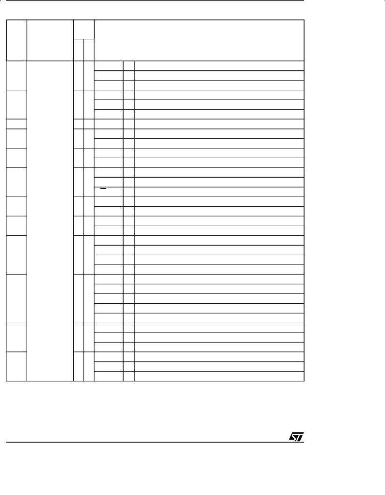
Table 7. Detailed Register Map
Page
No.
System
0
2
3
|
Reg. |
Register |
|
Reset |
Doc. |
|
Block |
Description |
Value |
||||
No. |
Name |
Page |
||||
|
|
Hex. |
||||
|
|
|
|
|
||
I/O |
R227 |
P3DR |
Port 3 Data Register |
FF |
|
|
|
|
|
|
|
||
Port |
R228 |
P4DR |
Port 4 Data Register |
FF |
98 |
|
|
|
|
|
|||
3:5 |
R229 |
P5DR |
Port 5 Data Register |
FF |
|
|
|
R230 |
CICR |
Central Interrupt Control Register |
87 |
30 |
|
|
R231 |
FLAGR |
Flag Register |
00 |
31 |
|
|
R232 |
RP0 |
Pointer 0 Register |
00 |
33 |
|
|
R233 |
RP1 |
Pointer 1 Register |
00 |
33 |
|
Core |
R234 |
PPR |
Page Pointer Register |
54 |
35 |
|
R235 |
MODER |
Mode Register |
E0 |
35 |
||
|
||||||
|
R236 |
USPHR |
User Stack Pointer High Register |
xx |
37 |
|
|
R237 |
USPLR |
User Stack Pointer Low Register |
xx |
37 |
|
|
R238 |
SSPHR |
System Stack Pointer High Reg. |
xx |
37 |
|
|
R239 |
SSPLR |
System Stack Pointer Low Reg. |
xx |
37 |
|
|
R242 |
EITR |
External Interrupt Trigger Register |
00 |
59 |
|
|
R243 |
EIPR |
External Interrupt Pending Reg. |
00 |
60 |
|
INT |
R244 |
EIMR |
External Interrupt Mask-bit Reg. |
00 |
60 |
|
R245 |
EIPLR |
External Interrupt Priority Level Reg. |
FF |
60 |
||
|
||||||
|
R246 |
EIVR |
External Interrupt Vector Register |
x6 |
61 |
|
|
R247 |
NICR |
Nested Interrupt Control |
00 |
61 |
|
|
R248 |
WDTHR |
Watchdog Timer High Register |
FF |
109 |
|
|
R249 |
WDTLR |
Watchdog Timer Low Register |
FF |
109 |
|
WDT |
R250 |
WDTPR |
Watchdog Timer Prescaler Reg. |
FF |
109 |
|
|
R251 |
WDTCR |
Watchdog Timer Control Register |
12 |
109 |
|
|
R252 |
WCR |
Wait Control Register |
7F |
110 |
|
I/O |
R252 |
P3C0 |
Port 3 Configuration Register 0 |
00 |
|
|
Port |
R253 |
P3C1 |
Port 3 Configuration Register 1 |
00 |
98 |
|
3 |
R254 |
P3C2 |
Port 3 Configuration Register 2 |
00 |
|
|
I/O |
R240 |
P4C0 |
Port 4 Configuration Register 0 |
00 |
|
|
Port |
R241 |
P4C1 |
Port 4 Configuration Register 1 |
00 |
|
|
4 |
R242 |
P4C2 |
Port 4 Configuration Register 2 |
00 |
|
|
I/O |
R244 |
P5C0 |
Port 5 Configuration Register 0 |
00 |
|
|
Port |
R245 |
P5C1 |
Port 5 Configuration Register 1 |
00 |
98 |
|
5 |
R246 |
P5C2 |
Port 5 Configuration Register 2 |
00 |
||
|
||||||
I/O |
R248 |
P6C0 |
Port 6 Configuration Register 0 |
00 |
|
|
R249 |
P6C1 |
Port 6 Configuration Register 1 |
00 |
|
||
Port |
|
|||||
R250 |
P6C2 |
Port 6 Configuration Register 2 |
00 |
|
||
6 |
|
|||||
R251 |
P6DR |
Port 6 Data Register |
FF |
|
||
|
|
22/224
ST92163 - GENERAL DESCRIPTION
Page |
|
Reg. |
Register |
|
Reset |
Doc. |
|
Block |
Description |
Value |
|||||
No. |
No. |
Name |
Page |
||||
|
|
Hex. |
|||||
|
|
|
|
|
|
||
|
|
R240 |
EP0RA |
Endpoint 0 Register A (Transmission) |
00 |
|
|
|
|
R241 |
EP0RB |
Endpoint 0 Register B (Reception) |
00 |
|
|
|
|
R242 |
EP1RA |
Endpoint 1 Register A (Transmission) |
00 |
|
|
|
|
R243 |
EP1RB |
Endpoint 1 Register B (Reception) |
00 |
|
|
|
|
R244 |
EP2RA |
Endpoint 2 Register A (Transmission) |
00 |
|
|
|
|
R245 |
EP2RB |
Endpoint 2 Register B (Reception) |
00 |
|
|
|
|
R246 |
EP3RA |
Endpoint 3 Register A (Transmission) |
00 |
|
|
4 |
|
R247 |
EP3RB |
Endpoint 3 Register B (Reception) |
00 |
|
|
|
R248 |
EP4RA |
Endpoint 4 Register A (Transmission) |
00 |
|
||
|
|
|
|||||
|
|
R249 |
EP4RB |
Endpoint 4 Register B (Reception) |
00 |
|
|
|
|
R250 |
EP5RA |
Endpoint 5 Register A (Transmission) |
00 |
|
|
|
|
R251 |
EP5RB |
Endpoint 5 Register B (Reception) |
00 |
|
|
|
|
R252 |
EP6RA |
Endpoint 6 Register A (Transmission) |
00 |
|
|
|
|
R253 |
EP6RB |
Endpoint 6 Register B (Reception) |
00 |
|
|
|
USB |
R254 |
EP7RA |
Endpoint 7 Register A (Transmission) |
00 |
|
|
|
R255 |
EP7RB |
Endpoint 7 Register B (Reception) |
00 |
|
||
|
End |
143 |
|||||
|
R240 |
EP8RA |
Endpoint 8 Register A (Transmission) |
00 |
|||
|
Points |
|
|||||
|
R241 |
EP8RB |
Endpoint 8 Register B (Reception) |
00 |
|
||
|
|
|
|||||
|
|
R242 |
EP9RA |
Endpoint 9 Register A (Transmission) |
00 |
|
|
|
|
R243 |
EP9RB |
Endpoint 9 Register B (Reception) |
00 |
|
|
|
|
R244 |
EP10RA |
Endpoint 10 Register A (Transmission) |
00 |
|
|
|
|
R245 |
EP10RB |
Endpoint 10 Register B (Reception) |
00 |
|
|
|
|
R246 |
EP11RA |
Endpoint 11 Register A (Transmission) |
00 |
|
|
5 |
|
R247 |
EP11RB |
Endpoint 11 Register B (Reception) |
00 |
|
|
|
R248 |
EP12RA |
Endpoint 12 Register A (Transmission) |
00 |
|
||
|
|
|
|||||
|
|
R249 |
EP12RB |
Endpoint 12 Register B (Reception) |
00 |
|
|
|
|
R250 |
EP13RA |
Endpoint 13 Register A (Transmission) |
00 |
|
|
|
|
R251 |
EP13RB |
Endpoint 13 Register B (Reception) |
00 |
|
|
|
|
R252 |
EP14RA |
Endpoint 14 Register A (Transmission) |
00 |
|
|
|
|
R253 |
EP14RB |
Endpoint 14 Register B (Reception) |
00 |
|
|
|
|
R254 |
EP15RA |
Endpoint 15 Register A (Transmission) |
00 |
|
|
|
|
R255 |
EP15RB |
Endpoint 15 Register B (Reception) |
00 |
|
|
|
|
R240 |
DCPR |
DMA Counter Pointer Register |
xx |
132 |
|
|
|
R241 |
DAPR |
DMA Address Pointer Register |
xx |
133 |
|
9 |
MFT |
R242 |
T_IVR |
Interrupt Vector Register |
xx |
133 |
|
|
|
R243 |
IDCR |
Interrupt/DMA Control Register |
C7 |
134 |
|
|
|
R248 |
IOCR |
I/O Connection Register |
FC |
134 |
23/224
ST92163 - GENERAL DESCRIPTION
Page |
|
Reg. |
Register |
|
Reset |
Doc. |
|
Block |
Description |
Value |
|||||
No. |
No. |
Name |
Page |
||||
|
|
Hex. |
|||||
|
|
|
|
|
|
||
|
|
R240 |
REG0HR |
Capture Load Register 0 High |
xx |
125 |
|
|
|
R241 |
REG0LR |
Capture Load Register 0 Low |
xx |
125 |
|
|
|
R242 |
REG1HR |
Capture Load Register 1 High |
xx |
125 |
|
|
|
R243 |
REG1LR |
Capture Load Register 1 Low |
xx |
125 |
|
|
|
R244 |
CMP0HR |
Compare 0 Register High |
00 |
125 |
|
|
|
R245 |
CMP0LR |
Compare 0 Register Low |
00 |
125 |
|
|
|
R246 |
CMP1HR |
Compare 1 Register High |
00 |
125 |
|
10 |
MFT |
R247 |
CMP1LR |
Compare 1 Register Low |
00 |
125 |
|
R248 |
TCR |
Timer Control Register |
0x |
126 |
|||
|
|
||||||
|
|
R249 |
TMR |
Timer Mode Register |
00 |
127 |
|
|
|
R250 |
T_ICR |
External Input Control Register |
0x |
128 |
|
|
|
R251 |
PRSR |
Prescaler Register |
00 |
128 |
|
|
|
R252 |
OACR |
Output A Control Register |
xx |
129 |
|
|
|
R253 |
OBCR |
Output B Control Register |
xx |
130 |
|
|
|
R254 |
T_FLAGR |
Flags Register |
00 |
31 |
|
|
|
R255 |
IDMR |
Interrupt/DMA Mask Register |
00 |
132 |
|
|
|
R240 |
DADDR0 |
Device Address Register 0 |
00 |
|
|
|
|
R241 |
DADDR1 |
Device Address Register 1 |
00 |
|
|
|
|
R242 |
DADDR2 |
Device Address Register 2 |
00 |
|
|
|
|
R243 |
DADDR3 |
Device Address Register 3 |
00 |
143 |
|
|
|
R244 |
DADDR4 |
Device Address Register 4 |
00 |
||
|
|
|
|||||
|
|
R245 |
DADDR5 |
Device Address Register 5 |
00 |
|
|
|
|
R246 |
DADDR6 |
Device Address Register 6 |
00 |
|
|
15 |
USB |
R247 |
DADDR7 |
Device Address Register 7 |
00 |
|
|
Common |
R248 |
USBIVR |
USB Interrupt Vector Register |
xx |
139 |
||
|
|||||||
|
|
R249 |
USBISTR |
USB Interrupt Status Register |
00 |
139 |
|
|
|
R250 |
USBIMR |
USB Interrupt Mask Register |
00 |
140 |
|
|
|
R251 |
USBIPR |
USB Interrupt Priority Register |
xx |
140 |
|
|
|
R252 |
USBCTLR |
USB Control Register |
17 |
141 |
|
|
|
R253 |
CTRINF |
CTR Interrrupt Flags |
xx |
142 |
|
|
|
R254 |
FNRH |
Frame Number Register High |
0x |
142 |
|
|
|
R255 |
FNRL |
Frame Number Register Low |
xx |
142 |
24/224

ST92163 - GENERAL DESCRIPTION
Page |
|
Reg. |
Register |
|
Reset |
Doc. |
|
Block |
Description |
Value |
|||||
No. |
No. |
Name |
Page |
||||
|
|
Hex. |
|||||
|
|
|
|
|
|
||
|
|
R240 |
I2CCR |
I2C Control Register |
00 |
186 |
|
|
|
R241 |
I2CSR1 |
I2C Status Register 1 |
00 |
187 |
|
|
|
R242 |
I2CSR2 |
I2C Status Register 2 |
00 |
189 |
|
|
|
R243 |
I2CCCR |
I2C Clock Control Register |
00 |
190 |
|
|
|
R244 |
I2COAR1 |
I2C Own Address Register 1 |
00 |
190 |
|
|
|
R245 |
I2COAR2 |
I2C Own Address Register 2 |
00 |
191 |
|
|
|
R246 |
I2CDR |
I2C Data Register |
00 |
191 |
|
20 |
I2C |
R247 |
I2CADR |
I2C General Call Address |
A0 |
191 |
|
R248 |
I2CISR |
I2C Interrupt Status Register |
xx |
192 |
|||
|
|
||||||
|
|
R249 |
I2CIVR |
I2C Interrupt Vector Register |
xx |
193 |
|
|
|
R250 |
I2CRDAP |
Receiver DMA Source Addr. Pointer |
xx |
193 |
|
|
|
R251 |
I2CRDC |
Receiver DMA Transaction Counter |
xx |
193 |
|
|
|
R252 |
I2CTDAP |
Transmitter DMA Source Addr. Pointer |
xx |
194 |
|
|
|
R253 |
I2CTDC |
Transmitter DMA Transaction Counter |
xx |
194 |
|
|
|
R254 |
I2CECCR |
I2C Extended Clock Control Register |
00 |
194 |
|
|
|
R255 |
I2CIMR |
I2C Interrupt Mask Register |
x0 |
195 |
|
|
|
R240 |
DPR0 |
Data Page Register 0 |
00 |
42 |
|
|
|
R241 |
DPR1 |
Data Page Register 1 |
01 |
42 |
|
|
|
R242 |
DPR2 |
Data Page Register 2 |
02 |
42 |
|
|
MMU |
R243 |
DPR3 |
Data Page Register 3 |
83 |
42 |
|
21 |
|
R244 |
CSR |
Code Segment Register |
00 |
43 |
|
|
|
R248 |
ISR |
Interrupt Segment Register |
x0 |
43 |
|
|
|
R249 |
DMASR |
DMA Segment Register |
x0 |
43 |
|
|
EXTMI |
R245 |
EMR1 |
External Memory Register 1 |
80 |
95 |
|
|
R246 |
EMR2 |
External Memory Register 2 |
0F |
96 |
||
|
|
||||||
|
|
R240 |
RDCPR |
Receiver DMA Transaction Counter Pointer |
xx |
165 |
|
|
|
R241 |
RDAPR |
Receiver DMA Source Address Pointer |
xx |
165 |
|
|
|
R242 |
TDCPR |
Transmitter DMA Transaction Counter Pointer |
xx |
165 |
|
|
|
R243 |
TDAPR |
Transmitter DMA Destination Address Pointer |
xx |
165 |
|
|
|
R244 |
S_IVR |
Interrupt Vector Register |
xx |
166 |
|
|
|
R245 |
ACR |
Address/Data Compare Register |
xx |
166 |
|
|
|
R246 |
IMR |
Interrupt Mask Register |
x0 |
167 |
|
|
|
R247 |
S_ISR |
Interrupt Status Register |
xx |
43 |
|
24 |
SCI |
R248 |
RXBR |
Receive Buffer Register |
xx |
169 |
|
|
|
R248 |
TXBR |
Transmitter Buffer Register |
xx |
169 |
|
|
|
R249 |
IDPR |
Interrupt/DMA Priority Register |
xx |
170 |
|
|
|
R250 |
CHCR |
Character Configuration Register |
xx |
171 |
|
|
|
R251 |
CCR |
Clock Configuration Register |
00 |
172 |
|
|
|
R252 |
BRGHR |
Baud Rate Generator High Reg. |
xx |
173 |
|
|
|
R253 |
BRGLR |
Baud Rate Generator Low Register |
xx |
173 |
|
|
|
R254 |
SICR |
Synchronous Input Control |
03 |
173 |
|
|
|
R255 |
SOCR |
Synchronous Output Control |
01 |
174 |
25/224
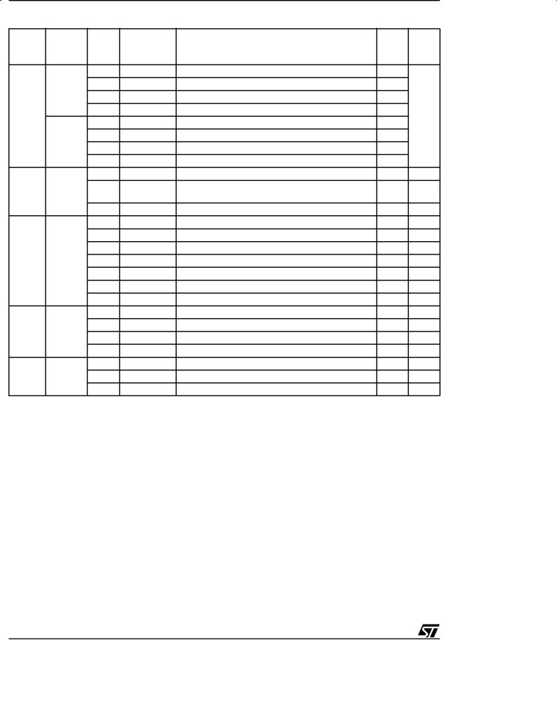
ST92163 - GENERAL DESCRIPTION
Page |
|
Reg. |
Register |
|
Reset |
Doc. |
|
Block |
Description |
Value |
|||||
No. |
No. |
Name |
Page |
||||
|
|
Hex. |
|||||
|
|
|
|
|
|
||
|
I/O |
R248 |
P8C0 |
Port 8 Configuration Register 0 |
00 |
|
|
|
R249 |
P8C1 |
Port 8 Configuration Register 1 |
00 |
|
||
|
Port |
|
|||||
|
R250 |
P8C2 |
Port 8 Configuration Register 2 |
00 |
|
||
|
8 |
|
|||||
|
R251 |
P8DR |
Port 8 Data Register |
FF |
|
||
43 |
|
98 |
|||||
|
R252 |
P9C0 |
Port 9 Configuration Register 0 |
00 |
|||
|
I/O |
|
|||||
|
R253 |
P9C1 |
Port 9 Configuration Register 1 |
00 |
|
||
|
Port |
|
|||||
|
R254 |
P9C2 |
Port 9 Configuration Register 2 |
00 |
|
||
|
9 |
|
|||||
|
R255 |
P9DR |
Port 9 Data Register |
FF |
|
||
|
|
|
|||||
|
|
R240 |
CLKCTL |
Clock Control Register |
00 |
81 |
|
55 |
RCCU |
R242 |
CLK_FLAG |
Clock Flag Register |
48, 28 |
82 |
|
or 08 |
|||||||
|
|
|
|
|
|
||
|
|
R246 |
PLLCONF |
PLL Configuration Register |
xx |
83 |
|
|
|
R249 |
WUCTRL |
Wake-Up Control Register |
00 |
67 |
|
|
|
R250 |
WUMRH |
Wake-Up Mask Register High |
00 |
68 |
|
|
|
R251 |
WUMRL |
Wake-Up Mask Register Low |
00 |
68 |
|
59 |
WUIMU |
R252 |
WUTRH |
Wake-Up Trigger Register High |
00 |
69 |
|
|
|
R253 |
WUTRL |
Wake-Up Trigger Register Low |
00 |
69 |
|
|
|
R254 |
WUPRH |
Wake-Up Pending Register High |
00 |
69 |
|
|
|
R255 |
WUPRL |
Wake-Up Pending Register Low |
00 |
69 |
|
|
|
R244 |
DEVCONF1 |
USB device configuration 1 |
0F |
146 |
|
60 |
USB |
R245 |
DEVCONF2 |
USB device configuration 2 |
00 |
146 |
|
R246 |
MIRRA |
Mirror Register A |
xx |
147 |
|||
|
|
||||||
|
|
R247 |
MIRRB |
Mirror Register B |
xx |
147 |
|
|
|
R240 |
ADDTR |
Channel i Data Register |
xx |
199 |
|
62 |
ADC |
R241 |
ADCLR |
Control Logic Register |
00 |
199 |
|
|
|
R242 |
ADINT |
AD Interrupt Register |
01 |
200 |
Note: xx denotes a byte with an undefined value, but some bits may have defined values. See register description for details.
26/224

ST92163 - DEVICE ARCHITECTURE
2 DEVICE ARCHITECTURE
2.1 CORE ARCHITECTURE
The ST9+ Core or Central Processing Unit (CPU) features a highly optimised instruction set, capable of handling bit, byte (8-bit) and word (16-bit) data, as well as BCD and Boolean formats; 14 addressing modes are available.
Four independent buses are controlled by the Core: a 16-bit Memory bus, an 8-bit Register data bus, an 8-bit Register address bus and a 6-bit Interrupt/DMA bus which connects the interrupt and DMA controllers in the on-chip peripherals with the Core.
This multiple bus architecture affords a high degree of pipelining and parallel operation, thus making the ST9+ family devices highly efficient, both for numerical calculation, data handling and with regard to communication with on-chip peripheral resources.
2.2 MEMORY SPACES
There are two separate memory spaces:
± The Register File, which comprises 240 8-bit registers, arranged as 15 groups (Group 0 to E), each containing sixteen 8-bit registers plus up to 64 pages of 16 registers mapped in Group F,
which hold data and control bits for the on-chip peripherals and I/Os.
± A single linear memory space accommodating both program and data. All of the physically separate memory areas, including the internal ROM, internal RAM and external memory are mapped in this common address space. The total addressable memory space of 4 Mbytes (limited by the size of on-chip memory and the number of external address pins) is arranged as 64 segments of 64 Kbytes. Each segment is further subdivided into four pages of 16 Kbytes, as illustrated in Figure 1. A Memory Management Unit uses a set of pointer registers to address a 22-bit memory field using 16-bit address-based instructions.
2.2.1 Register File
The Register File consists of (see Figure 2):
±224 general purpose registers (Group 0 to D, registers R0 to R223)
±6 system registers in the System Group (Group E, registers R224 to R239)
±Up to 64 pages, depending on device configuration, each containing up to 16 registers, mapped to Group F (R240 to R255), see Figure 3.
|
|
Data |
Code |
Address |
|
16K Pages |
64K Segments |
3FFFFFh |
|
255 |
|
|
|
254 |
63 |
|
|
253 |
|
3F0000h |
|
|
|
|
252 |
|
|
3EFFFFh |
|
251 |
|
|
|
250 |
62 |
3E0000h |
|
249 |
|
|
248 |
|
|
|
|
247 |
|
up to 4 Mbytes |
|
|
|
21FFFFh |
|
135 |
|
Reserved |
134 |
|
|
|
33 |
||
|
133 |
||
210000h |
|
||
|
132 |
|
|
20FFFFh |
|
|
|
02FFFFh |
|
11 |
|
|
10 |
|
|
|
|
2 |
|
020000h |
|
9 |
|
|
|
||
|
8 |
|
|
01FFFFh |
|
7 |
|
|
6 |
1 |
|
|
|
||
010000h |
|
5 |
|
|
|
||
|
4 |
|
|
00FFFFh |
|
3 |
|
Figure 7. Single Program and Data Memory Address Space |
2 |
|
|
|
|
000000h |
1 |
0 |
|
||
0 |
|
|
|
|
27/224
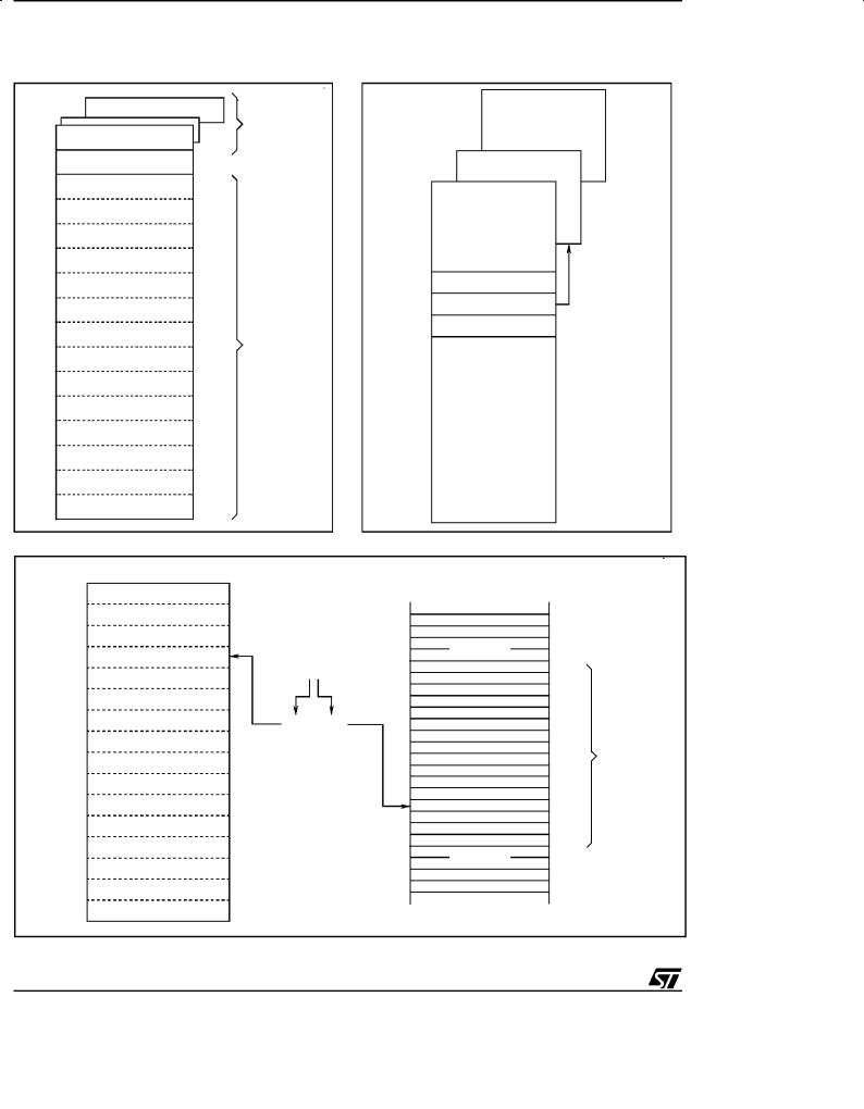
ST92163 - DEVICE ARCHITECTURE
MEMORY SPACES (Cont'd) |
|
|
|
||
Figure 8. Register Groups |
|
Figure 9. Page Pointer for Group F mapping |
|||
|
|
|
UP TO |
|
PAGE 63 |
255 |
|
|
|
|
|
|
|
64 PAGES |
|
|
|
240 F PAGED REGISTERS |
|
|
|||
|
|
|
|||
239 |
E SYSTEM REGISTERS |
|
|
PAGE 5 |
|
224 |
|
|
|||
223 |
D |
|
|
R255 |
|
|
C |
|
|
|
PAGE 0 |
|
|
|
|
|
|
|
B |
|
|
|
|
|
A |
|
|
R240 |
|
|
|
|
|
|
|
|
9 |
|
|
|
|
|
8 |
|
|
R234 |
PAGE POINTER |
|
|
224 |
|
|
|
|
7 |
|
R224 |
|
|
|
|
GENERAL |
|
||
|
|
|
|
|
|
|
6 |
|
PURPOSE |
|
|
|
|
REGISTERS |
|
|
|
|
|
|
|
|
|
|
5 |
|
|
|
|
|
4 |
|
|
|
|
|
3 |
|
|
|
|
|
2 |
|
|
|
|
|
1 |
|
|
|
|
|
0 |
15 |
|
|
|
0 |
0 |
VA00432 |
R0 |
|
|
|
VA00433 |
||||
Figure 10. Addressing the Register File |
|
|
|||
|
|
REGISTER FILE |
|
|
|
|
255 |
F PAGED REGISTERS |
|
|
|
|
240 |
|
|
|
|
|
|
|
|
|
|
|
239 |
E SYSTEM REGISTERS |
|
|
|
|
224 |
|
|
|
|
|
|
|
|
|
|
|
223 |
D |
|
|
|
|
|
|
|
GROUP D |
|
|
|
C |
R195 |
|
|
|
|
|
R207 |
||
|
|
|
|
||
|
|
|
(R0C3h) |
|
|
|
|
B |
|
|
|
|
|
|
|
|
|
|
|
A |
|
|
|
|
|
9 |
(1100) (0011) |
|
|
|
|
|
|
|
|
|
|
8 |
|
|
|
|
|
7 |
|
|
GROUP C |
|
|
|
|
|
|
|
|
6 |
|
|
|
|
|
5 |
|
|
R195 |
|
|
4 |
|
|
|
|
|
3 |
|
|
R192 |
|
|
|
|
GROUP B |
|
|
|
2 |
|
|
|
|
|
|
|
|
|
|
|
1 |
|
|
|
|
|
0 |
15 |
|
|
|
0 |
0 |
|
|
|
|
|
|
VR000118 |
||
|
|
|
|
|
|
28/224

MEMORY SPACES (Cont'd)
2.2.2 Register Addressing
Register File registers, including Group F paged registers (but excluding Group D), may be addressed explicitly by means of a decimal, hexadecimal or binary address; thus R231, RE7h and R11100111b represent the same register (see Figure 4). Group D registers can only be addressed in Working Register mode.
Note that an upper case ªRº is used to denote this direct addressing mode.
Working Registers
Certain types of instruction require that registers be specified in the form ªrxº, where x is in the range 0 to 15: these are known as Working Registers.
Note that a lower case ªrº is used to denote this indirect addressing mode.
Two addressing schemes are available: a single group of 16 working registers, or two separately mapped groups, each consisting of 8 working registers. These groups may be mapped starting at any 8 or 16 byte boundary in the register file by means of dedicated pointer registers. This technique is described in more detail in Section 1.3.3, and illustrated in Figure 5 and in Figure 6.
System Registers
The 16 registers in Group E (R224 to R239) are System registers and may be addressed using any of the register addressing modes. These registers are described in greater detail in Section 1.3.
Paged Registers
Up to 64 pages, each containing 16 registers, may be mapped to Group F. These are addressed using any register addressing mode, in conjunction with the Page Pointer register, R234, which is one of the System registers. This register selects the page to be mapped to Group F and, once set, does not need to be changed if two or more registers on the same page are to be addressed in succession.
ST92163 - DEVICE ARCHITECTURE
Therefore if the Page Pointer, R234, is set to 5, the instructions:
spp #5
ld R242, r4
will load the contents of working register r4 into the third register of page 5 (R242).
These paged registers hold data and control information relating to the on-chip peripherals, each peripheral always being associated with the same pages and registers to ensure code compatibility between ST9+ devices. The number of these registers therefore depends on the peripherals which are present in the specific ST9+ family device. In other words, pages only exist if the relevant peripheral is present.
Table 8. Register File Organization
Hex. |
Decimal |
Function |
Register |
|
Address |
Address |
File Group |
||
|
||||
F0-FF |
240-255 |
Paged |
Group F |
|
Registers |
||||
|
|
|
||
E0-EF |
224-239 |
System |
Group E |
|
Registers |
||||
|
|
|
||
D0-DF |
208-223 |
|
Group D |
|
C0-CF |
192-207 |
|
Group C |
|
B0-BF |
176-191 |
|
Group B |
|
A0-AF |
160-175 |
|
Group A |
|
90-9F |
144-159 |
|
Group 9 |
|
80-8F |
128-143 |
|
Group 8 |
|
70-7F |
112-127 |
General |
Group 7 |
|
Purpose |
||||
60-6F |
96-111 |
Group 6 |
||
Registers |
||||
|
|
|
||
50-5F |
80-95 |
|
Group 5 |
|
40-4F |
64-79 |
|
Group 4 |
|
30-3F |
48-63 |
|
Group 3 |
|
20-2F |
32-47 |
|
Group 2 |
|
10-1F |
16-31 |
|
Group 1 |
|
00-0F |
00-15 |
|
Group 0 |
29/224
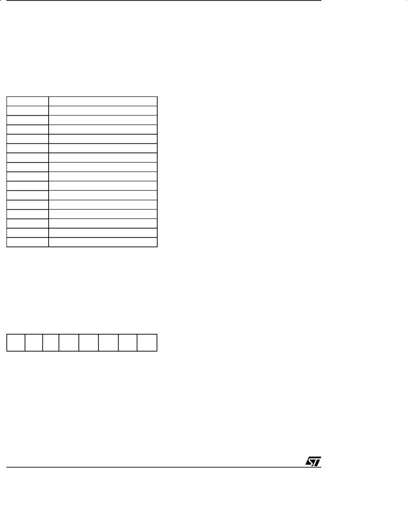
ST92163 - DEVICE ARCHITECTURE
2.3 SYSTEM REGISTERS
The System registers are listed in Table 2 System Registers (Group E). They are used to perform all the important system settings. Their purpose is described in the following pages. Refer to the chapter dealing with I/O for a description of the PORT[5:0] Data registers.
Table 9. System Registers (Group E)
R239 |
(EFh) |
SSPLR |
R238 |
(EEh) |
SSPHR |
R237 |
(EDh) |
USPLR |
R236 |
(ECh) |
USPHR |
R235 |
(EBh) |
MODE REGISTER |
R234 |
(EAh) |
PAGE POINTER REGISTER |
R233 |
(E9h) |
REGISTER POINTER 1 |
R232 |
(E8h) |
REGISTER POINTER 0 |
R231 |
(E7h) |
FLAG REGISTER |
R230 |
(E6h) |
CENTRAL INT. CNTL REG |
R229 |
(E5h) |
PORT5 DATA REG. |
R228 |
(E4h) |
PORT4 DATA REG. |
R227 |
(E3h) |
PORT3 DATA REG. |
R226 |
(E2h) |
PORT2 DATA REG. |
R225 |
(E1h) |
PORT1 DATA REG. |
R224 |
(E0h) |
PORT0 DATA REG. |
2.3.1 Central Interrupt Control Register
Please refer to the ºINTERRUPTº chapter for a detailed description of the ST9 interrupt philosophy.
CENTRAL INTERRUPT CONTROL REGISTER (CICR)
R230 - Read/Write Register Group: E (System)
Reset Value: 1000 0111 (87h)
7 |
0 |
GCEN TLIP TLI IEN IAM CPL2 CPL1 CPL0
Bit 7 = GCEN: Global Counter Enable.
This bit is the Global Counter Enable of the Multifunction Timers. The GCEN bit is ANDed with the CE bit in the TCR Register (only in devices featuring the MFT Multifunction Timer) in order to enable the Timers when both bits are set. This bit is set after the Reset cycle.
Note: If an MFT is not included in the ST9 device, then this bit has no effect.
Bit 6 = TLIP: Top Level Interrupt Pending.
This bit is set by hardware when a Top Level Interrupt Request is recognized. This bit can also be set by software to simulate a Top Level Interrupt Request.
0:No Top Level Interrupt pending
1:Top Level Interrupt pending
Bit 5 = TLI: Top Level Interrupt bit.
0:Top Level Interrupt is acknowledged depending on the TLNM bit in the NICR Register.
1:Top Level Interrupt is acknowledged depending on the IEN and TLNM bits in the NICR Register (described in the Interrupt chapter).
Bit 4 = IEN: Interrupt Enable .
This bit is cleared by interrupt acknowledgement, and set by interrupt return (iret). IEN is modified implicitly by iret, ei and di instructions or by an interrupt acknowledge cycle. It can also be explicitly written by the user, but only when no interrupt is pending. Therefore, the user should execute a di instruction (or guarantee by other means that no interrupt request can arrive) before any write operation to the CICR register.
0:Disable all interrupts except Top Level Interrupt.
1:Enable Interrupts
Bit 3 = IAM: Interrupt Arbitration Mode.
This bit is set and cleared by software to select the arbitration mode.
0:Concurrent Mode
1:Nested Mode.
Bit 2:0 = CPL[2:0]: Current Priority Level.
These three bits record the priority level of the routine currently running (i.e. the Current Priority Level, CPL). The highest priority level is represented by 000, and the lowest by 111. The CPL bits can be set by hardware or software and provide the reference according to which subsequent interrupts are either left pending or are allowed to interrupt the current interrupt service routine. When the current interrupt is replaced by one of a higher priority, the current priority value is automatically stored until required in the NICR register.
30/224
 Loading...