


DISCRETE SEMICONDUCTORS
DATA SHEET
M3D071
BCV62
PNP general purpose double transistor
Product specification |
|
1999 Apr 08 |
|||||
Supersedes data of 1997 Jun 18 |
|
|
|
|
|
|
|
|
|
|
|
|
|
|
|
|
|
|
|
|
|
|
|
|
|
|
|
|
|
|
|
Philips Semiconductors |
Product specification |
|
|
PNP general purpose double transistor |
BCV62 |
|
|
|
|
FEATURES
∙Low current (max. 100 mA)
∙Low voltage (max. 30 V)
∙Matched pair.
APPLICATIONS
∙For use in applications where the working point must be independent of temperature
∙Current mirrors.
DESCRIPTION
PNP double transistor in a SOT143B plastic package. NPN complement: BCV61.
MARKING
TYPE |
MARKING |
TYPE |
MARKING |
NUMBER |
CODE |
NUMBER |
CODE |
|
|
|
|
BCV62 |
3Mp |
BCV62B |
3Kp |
|
|
|
|
BCV62A |
3Jp |
BCV62C |
3Lp |
|
|
|
|
LIMITING VALUES
PINNING
PIN |
DESCRIPTION |
|
|
1 |
collector TR2; base TR1 and TR2 |
|
|
2 |
collector TR1 |
|
|
3 |
emitter TR1 |
|
|
4 |
emitter TR2 |
|
|
|
|
|
3 |
|
|
|
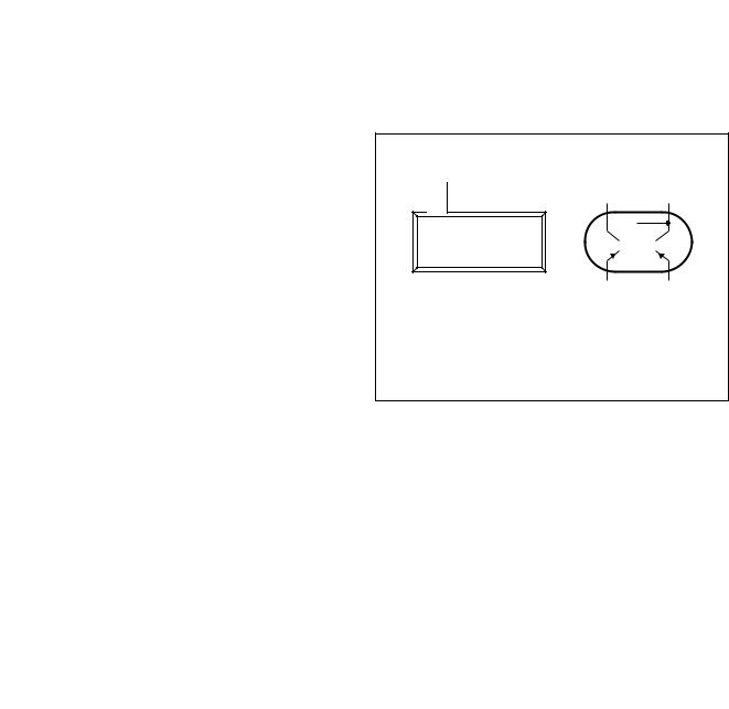
handbook, |
halfpage |
|
|
|
||
|
4 |
|
2 |
1 |
||
|
|
|
|
|
||
|
|
|
|
|
|
|
TR1 

 TR2
TR2
|
|
1 |
2 |
|
3 |
4 |
|
|
|
||||
|
|
|
|
|
||
|
|
|
|
|
|
|
Top view |
|
|
MAM292 |
|
||
Fig.1 Simplified outline (SOT143B) and symbol.
In accordance with the Absolute Maximum Rating System (IEC 134).
SYMBOL |
PARAMETER |
CONDITIONS |
MIN. |
MAX. |
UNIT |
|
|
|
|
|
|
VCBO |
collector-base voltage TR1 |
open emitter |
− |
−30 |
V |
VCEO |
collector-emitter voltage TR1 |
open base |
− |
−30 |
V |
VEBS |
emitter-base voltage |
VCE = 0 |
− |
−6 |
V |
IC |
collector current (DC) |
|
− |
−100 |
mA |
ICM |
peak collector current |
|
− |
−200 |
mA |
IBM |
peak base current TR1 |
|
− |
−200 |
mA |
Ptot |
total power dissipation |
Tamb ≤ 25 °C; note 1 |
− |
250 |
mW |
Tstg |
storage temperature |
|
−65 |
+150 |
°C |
Tj |
junction temperature |
|
− |
150 |
°C |
Tamb |
operating ambient temperature |
|
−65 |
+150 |
°C |
Note
1. Device mounted on an FR4 printed-circuit board.
1999 Apr 08 |
2 |

Philips Semiconductors |
|
Product specification |
||
|
|
|
|
|
PNP general purpose double transistor |
|
|
BCV62 |
|
|
|
|
|
|
THERMAL CHARACTERISTICS |
|
|
|
|
|
|
|
|
|
SYMBOL |
PARAMETER |
CONDITIONS |
VALUE |
UNIT |
|
|
|
|
|
Rth j-a |
thermal resistance from junction to ambient |
note 1 |
500 |
K/W |
Note
1. Device mounted on an FR4 printed-circuit board.
CHARACTERISTICS
Tj = 25 °C unless otherwise specified.
SYMBOL |
PARAMETER |
CONDITIONS |
MIN. |
TYP. |
MAX. |
UNIT |
|
|
|
|
|
|
|
Transistor TR1 |
|
|
|
|
|
|
|
|
|
|
|
|
|
ICBO |
collector cut-off current |
IE = 0; VCB = −30 V |
− |
− |
−15 |
nA |
|
|
IE = 0; VCB = −30 V; Tj = 150 °C |
− |
− |
−5 |
μA |
IEBO |
emitter cut-off current |
IC = 0; VEB = −5 V |
− |
− |
−100 |
nA |
hFE |
DC current gain |
IC = −100 μA; VCE = −5 V |
100 |
− |
− |
|
|
|
IC = −2 mA; VCE = −5 V |
100 |
− |
800 |
|
VCEsat |
collector-emitter saturation |
IC = −10 mA; IB = −0.5 mA |
− |
−75 |
−300 |
mV |
|
voltage |
IC = −100 mA; IB = −5 mA |
− |
−250 |
−650 |
mV |
VBEsat |
base-emitter saturation |
IC = −10 mA; IB =− 0.5 mA; note 1 |
− |
−700 |
− |
mV |
|
voltage |
IC = −100 mA; IB = −5 mA; note 1 |
− |
−850 |
− |
mV |
VBE |
base-emitter voltage |
IC = −2 mA; VCE = −5 V; note 1 |
−600 |
−650 |
−750 |
mV |
|
|
IC = −10 mA; VCE = −5 V; note 2 |
− |
− |
−820 |
mV |
Cc |
collector capacitance |
IE = ie = 0; VCB = −10 V |
− |
4.5 |
− |
pF |
fT |
transition frequency |
IC = −10 mA; VCE = −5 V; f = 100 MHz |
100 |
− |
− |
MHz |
F |
noise figure |
IC = −200 μA; VCE = −5 V; RS = 2 kΩ; |
− |
− |
10 |
dB |
|
|
f = 1 kHz; B = 200 Hz |
|
|
|
|
|
|
|
|
|
|
|
Transistor TR2 |
|
|
|
|
|
|
|
|
|
|
|
|
|
VEBS |
base-emitter forward voltage |
IE = 250 mA; VCB = 0 |
− |
− |
1.5 |
V |
|
|
IE = 10 μA; VCB = 0 |
400 |
− |
− |
mV |
hFE |
DC current gain |
IC = −2 mA; VCE = −5 V |
|
|
|
|
|
BCV62A |
|
125 |
− |
250 |
|
|
BCV62B |
|
220 |
− |
475 |
|
|
BCV62C |
|
420 |
− |
800 |
|
|
|
|
|
|
|
|
1999 Apr 08 |
3 |
 Loading...