


DISCRETE SEMICONDUCTORS
DATA SHEET
ook, halfpage
M3D087
BAT140 series
Schottky barrier double diodes
Product specification |
|
1997 Oct 03 |
|||||
File under Discrete Semiconductors, SC01 |
|
|
|
|
|
|
|
|
|
|
|
|
|
|
|
|
|
|
|
|
|
|
|
|
|
|
|
|
|
|
|
Philips Semiconductors |
Product specification |
|
|
Schottky barrier double diodes |
BAT140 series |
|
|
|
|
FEATURES
∙Low switching losses
∙Capability of absorbing very high surge current
∙Fast recovery time
∙Guard ring protected
∙Plastic SMD package.
APPLICATIONS
∙Low power switched-mode power supplies
∙Rectification
∙Polarity protection.
DESCRIPTION
Planar Schottky barrier double diodes encapsulated in a SOT223 plastic SMD package.
MARKING
TYPE NUMBER |
MARKING |
|
CODE |
||
|
||
|
|
|
BAT140A |
AT140A |
|
|
|
|
BAT140C |
AT140C |
|
|
|
|
BAT140S |
AT140S |
|
|
|
PINNING
PIN |
|
|
BAT140 |
|
||
|
|
|
|
|
||
A |
C |
S |
||||
|
||||||
|
|
|
|
|
|
|
1 |
k1 |
a1 |
a1 |
|||
2 |
n.c. |
n.c. |
n.c. |
|||
|
|
|
|
|
|
|
3 |
k2 |
a2 |
k2 |
|||
4 |
a1, a2 |
k1, k2 |
k1, a2 |
|||
|
|
|
|
|
|
|
age |
|
|
|
4 |
|
|
|
|
|
|
|||
|
|
|
|
|
|
|
|
|
1 |
|
2 |
|
|
3 |
Top view |
|
|
MSB002 - 1 |
||||
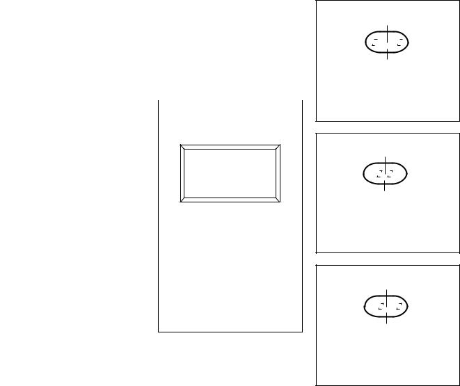
Fig.1 Simplified outline (SOT223) and pin configuration.
4
page
1 


 3
3
2 n.c. MGL171
Fig.2 BAT140A diode configuration (symbol).
4
page
1 


 3
3
2 n.c. MGL172
Fig.3 BAT140C diode configuration (symbol).
4
page
1 


 3
3
2 n.c. MGL173
Fig.4 BAT140S diode configuration (symbol).
1997 Oct 03 |
2 |

Philips Semiconductors |
|
|
Product specification |
||
|
|
|
|
|
|
Schottky barrier double diodes |
|
BAT140 series |
|||
|
|
|
|
|
|
LIMITING VALUES |
|
|
|
|
|
In accordance with the Absolute Maximum Rating System (IEC 134). |
|
|
|
||
|
|
|
|
|
|
SYMBOL |
PARAMETER |
CONDITIONS |
MIN. |
MAX. |
UNIT |
|
|
|
|
|
|
Per diode |
|
|
|
|
|
|
|
|
|
|
|
VR |
continuous reverse voltage |
|
− |
40 |
V |
IF |
continuous forward current |
|
− |
1 |
A |
IF(AV) |
average forward current |
Tamb = 65 °C; |
− |
1 |
A |
|
|
Rth j-a = 80 K/W; note 1; |
|
|
|
|
|
VR(equiv) = 0.2 V; note 2 |
|
|
|
IFSM |
non-repetitive peak forward current |
t = 8.3 μs half sinewave; |
− |
10 |
A |
|
|
JEDEC method |
|
|
|
|
|
|
|
|
|
IRSM |
non-repetitive peak reverse current |
tp = 100 μs |
− |
0.5 |
A |
Tstg |
storage temperature |
|
−65 |
+150 |
°C |
Tj |
junction temperature |
|
− |
125 |
°C |
Notes
1.Refer to SOT223 standard mounting conditions.
2.For Schottky barrier diodes thermal run-away has to be considered, as in some applications, the reverse power
losses PR are a significant part of the total power losses. Nomograms for determination of the reverse power losses PR and IF(AV) rating will be available on request.
ELECTRICAL CHARACTERISTICS
Tamb = 25 °C unless otherwise specified.
SYMBOL |
PARAMETER |
CONDITIONS |
TYP. |
MAX. |
UNIT |
|
|
|
|
|
|
Per diode |
|
|
|
|
|
|
|
|
|
|
|
VF |
forward voltage |
see Fig.5 |
|
|
|
|
|
IF = 100 mA; note 1 |
280 |
330 |
mV |
|
|
IF = 1 A; note 1 |
460 |
500 |
mV |
IR |
reverse current |
VR = 10 V; note 1; see Fig.6 |
15 |
40 |
μA |
|
|
VR = 40 V; note 1; see Fig.6 |
60 |
300 |
μA |
Cd |
diode capacitance |
VR = 4 V; f = 1 MHz; see Fig.7 |
65 |
80 |
pF |
Note
1. Pulsed test: tp = 300 μs; δ = 0.02.
THERMAL CHARACTERISTICS
SYMBOL |
PARAMETER |
CONDITIONS |
VALUE |
UNIT |
|
|
|
|
|
Rth j-a |
thermal resistance from junction to ambient |
note 1 |
100 |
K/W |
Note |
|
|
|
|
1. Refer to SOT223 standard mounting conditions.
1997 Oct 03 |
3 |
 Loading...