


DISCRETE SEMICONDUCTORS
DATA SHEET
age
M3D088
BAT754 series
Schottky barrier (double) diodes
Product specification |
|
1999 Aug 05 |
|||||
|
|
|
|
|
|
|
|
|
|
|
|
|
|
|
|
|
|
|
|
|
|
|
|
Philips Semiconductors |
Product specification |
|
|
Schottky barrier (double) diodes |
BAT754 series |
|
|
|
|
FEATURES
∙Very low forward voltage
∙Guard ring protected
∙Small plastic SMD package
∙Low diode capacitance.
APPLICATIONS
∙Ultra high-speed switching
∙Voltage clamping
∙Protection circuits
∙Blocking diodes
∙Low power consumption applications, e.g. hand-held applications.
DESCRIPTION
Planar Schottky barrier diodes encapsulated in a SOT23 small plastic SMD package. Low forward voltage selection of the BAT54 series. Single diodes and double diodes with different pinning are available.
MARKING
TYPE |
MARKING |
NUMBER |
CODE |
|
|
BAT754 |
2K |
|
|
BAT754A |
2L |
|
|
BAT754C |
2M |
|
|
BAT754S |
2N |
|
|
PINNING
PIN |
|
|
|
|
|
BAT754 |
|
|||||
|
|
|
|
|
|
|
|
|
|
|
|
|
|
|
|
|
|
A |
|
C |
|
S |
|||
|
|
|
|
|
|
|
|
|||||
|
|
|
|
|
|
|
|
|
|
|
|
|
1 |
|
a |
|
|
k1 |
|
a1 |
|
a1 |
|||
2 |
|
n.c. |
|
|
k2 |
|
a2 |
|
k2 |
|||
3 |
|
k |
|
a1, a2 |
k1, k2 |
k1, a2 |
||||||
|
|
|
|
|
|
|
|
|
|
|
|
|
|
|
|
1 |
|
|
3 |
|
2 |
|
|||
|
|
|
|
|
|
|
||||||
|
|
|
|
|
|
|
|
|
||||
|
|
|
|
|
|
|
|
|
||||
|
|
|
|
|
|
|
|
|
||||
|
|
|
|
|
|
|
|
|
||||
|
|
|
|
|
|
|
|
|
|
|||
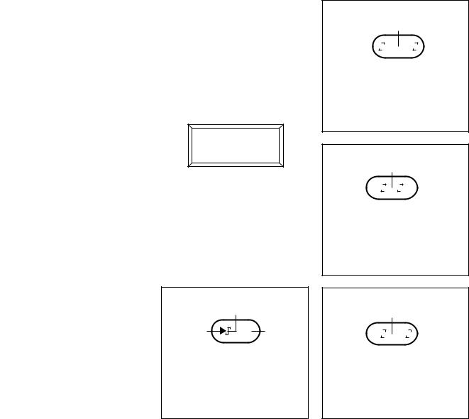
Top view |
|
|
|
|
MGC421 |
|
||||||
Fig.1 |
Simplified outline |
|
||||||||||
|
|
(SOT23) and pin |
|
|||||||||
|
|
configuration. |
|
|
|
|
||||||
|
|
|
|
|
|
|
|
|
|
|
|
|
|
3 |
1 |
2 |
n.c.
MLC357
Fig.2 BAT754 single diode configuration (symbol).
3
1 

 2
2
MLC360
Fig.3 BAT754A diode configuration (symbol).
3
1 


 2
2
MLC359
Fig.4 BAT754C diode configuration (symbol).
3
1 


 2
2
MLC358
Fig.5 BAT754S diode configuration (symbol).
1999 Aug 05 |
2 |

Philips Semiconductors |
|
Product specification |
|||
|
|
|
|
|
|
Schottky barrier (double) diodes |
|
BAT754 series |
|||
|
|
|
|
|
|
LIMITING VALUES |
|
|
|
|
|
In accordance with the Absolute Maximum Rating System (IEC 134). |
|
|
|
||
|
|
|
|
|
|
SYMBOL |
PARAMETER |
CONDITIONS |
MIN. |
MAX. |
UNIT |
|
|
|
|
|
|
Per diode |
|
|
|
|
|
|
|
|
|
|
|
VR |
continuous reverse voltage |
|
− |
30 |
V |
IF |
continuous forward current |
|
− |
200 |
mA |
IFRM |
repetitive peak forward current |
tp ≤ 1 s; δ ≤ 0.5 |
− |
300 |
mA |
IFSM |
non-repetitive peak forward current |
t = 8.3 ms half sinewave; |
− |
600 |
mA |
|
|
JEDEC method |
|
|
|
|
|
|
|
|
|
Tstg |
storage temperature |
|
−65 |
+150 |
°C |
Tj |
junction temperature |
|
− |
125 |
°C |
Tamb |
operating ambient temperature |
|
−65 |
+125 |
°C |
ELECTRICAL CHARACTERISTICS
Tamb = 25 °C unless otherwise specified.
SYMBOL |
PARAMETER |
CONDITIONS |
TYP. |
MAX. |
UNIT |
|
|
|
|
|
|
Per diode |
|
|
|
|
|
|
|
|
|
|
|
VF |
forward voltage |
see Fig.6 |
|
|
|
|
|
IF = 0.1 mA |
− |
200 |
mV |
|
|
IF = 1 mA |
− |
260 |
mV |
|
|
IF = 10 mA |
− |
340 |
mV |
|
|
IF = 30 mA |
− |
420 |
mV |
|
|
IF = 100 mA |
600 |
− |
mV |
IR |
reverse current |
VR = 25 V; note 1; see Fig.7 |
− |
2 |
μA |
Cd |
diode capacitance |
f = 1 MHz; VR = 1 V; see Fig.8 |
− |
10 |
pF |
Note
1. Pulse test: tp = 300 μs; δ ≤ 0.02.
THERMAL CHARACTERISTICS
SYMBOL |
PARAMETER |
CONDITIONS |
VALUE |
UNIT |
|
|
|
|
|
Rth j-a |
thermal resistance from junction to |
note 1 |
500 |
K/W |
|
ambient |
|
|
|
|
|
|
|
|
Note |
|
|
|
|
1. Refer to SOT23 standard mounting conditions.
1999 Aug 05 |
3 |
 Loading...