


BC857BW
Philips BC857BW, BC857W, BC857CW, BC857AW, BC856W Datasheet
...
DATA SH EET
Product specification
Supersedes data of 1997 Apr 07
1999 Apr 12
DISCRETE SEMICONDUCTORS
BC856W; BC857W
PNP general purpose transistors
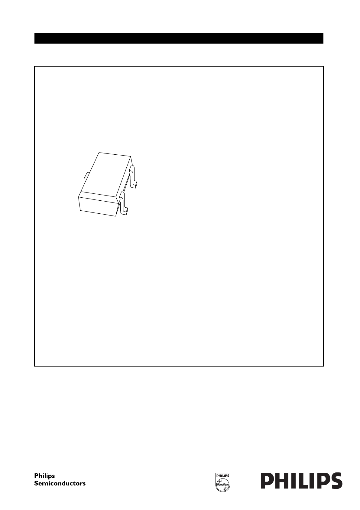
andbook, halfpage
M3D187

1999 Apr 12 2
Philips Semiconductors Product specification
PNP general purpose transistors BC856W; BC857W
FEATURES
• Low current (max. 100 mA)
• Low voltage (max. 80)
• S-mini package.
APPLICATIONS
• General purpose switching and amplification.
DESCRIPTION
PNP transistor in a plastic SOT323 package.
NPN complements: BC846W and BC847W.
MARKING
Note
1. ∗ = - : Made in Hong Kong.
∗ = t : Made in Malaysia.
TYPE
NUMBER
MARKING
CODE
(1)
TYPE
NUMBER
MARKING
CODE
(1)
BC856W 3D∗ BC857AW 3E∗
BC856AW 3A∗ BC857BW 3F∗
BC856BW 3B∗ BC857CW 3G∗
BC857W 3H∗
PINNING
PIN DESCRIPTION
1 base
2 emitter
3 collector
Fig.1 Simplified outline (SOT323) and symbol.
handbook, halfpage
MAM048
Top view
2
1
3
2
3
1

1999 Apr 12 3
Philips Semiconductors Product specification
PNP general purpose transistors BC856W; BC857W
LIMITING VALUES
In accordance with the Absolute Maximum Rating System (IEC 134).
Note
1. Transistor mounted on an FR4 printed-circuit board.
SYMBOL PARAMETER CONDITIONS MIN. MAX. UNIT
V
CBO
collector-base voltage open emitter
BC856W −−80 V
BC857W −−50 V
V
CEO
collector-emitter voltage open base
BC856W −−65 V
BC857W −−45 V
V
EBO
emitter-base voltage open collector −−5V
I
C
collector current (DC) −−100 mA
I
CM
peak collector current −−200 mA
I
BM
peak base current −−200 mA
P
tot
total power dissipation T
amb
≤ 25 °C; note 1 − 200 mW
T
stg
storage temperature −65 +150 °C
T
j
junction temperature − 150 °C
T
amb
operating ambient temperature −65 +150 °C

1999 Apr 12 4
Philips Semiconductors Product specification
PNP general purpose transistors BC856W; BC857W
THERMAL CHARACTERISTICS
Note
1. Transistor mounted on an FR4 printed-circuit board.
CHARACTERISTICS
T
amb
=25°C unless otherwise specified.
Note
1. Pulse test: t
p
≤ 300 µs; δ≤0.02.
SYMBOL PARAMETER CONDITIONS VALUE UNIT
R
th j-a
thermal resistance from junction to ambient note 1 625 K/W
SYMBOL PARAMETER CONDITIONS MIN. MAX. UNIT
I
CBO
collector cut-off current I
E
= 0; V
CB
= −30 V −−15 nA
I
E
= 0; V
CB
= −30 V; T
j
= 150 °C −−4µA
I
EBO
emitter cut-off current I
C
= 0; V
EB
= −5V −−100 nA
h
FE
DC current gain I
C
= −2 mA; V
CE
= −5V;
see Figs 2, 3 and 4
BC856W 125 475
BC857W 125 800
BC856AW; BC857AW 125 250
BC856BW; BC857BW 220 475
BC857CW 420 800
V
CEsat
collector-emitter saturation voltage I
C
= −10 mA; I
B
= −0.5 mA −−300 mV
I
C
= −100 mA; I
B
= −5 mA; note 1 −−650 mV
V
BEsat
base-emitter saturation voltage I
C
= −100 mA; I
B
= −5 mA; note 1 −−950 mV
V
BE
base-emitter voltage I
C
= −2 mA; V
CE
= −5V −600 −750 mV
I
C
= −10 mA; V
CE
= −5V −−820 mV
C
c
collector capacitance I
E
=i
e
= 0; V
CB
= −10 V; f = 1 MHz − 5pF
C
e
emitter capacitance I
C
=i
c
=0; V
EB
= −0.5 V; f = 1 MHz − 12 pF
f
T
transition frequency I
C
= −10 mA; V
CE
= −5 V; f = 100 MHz 100 − MHz
F noise figure I
C
= −200 µA; V
CE
= −5 V; R
S
=2kΩ;
f = 1 kHz; B = 200 Hz
− 10 dB
 Loading...