


DISCRETE SEMICONDUCTORS
DATA SHEET
age
M3D088
M3D071
BAS40 series
Schottky barrier (double) diodes
Product specification |
|
1999 Apr 28 |
|||||
Supersedes data of 1997 Oct 24 |
|
|
|
|
|
|
|
|
|
|
|
|
|
|
|
|
|
|
|
|
|
|
|
|
|
|
|
|
|
|
|
Philips Semiconductors |
Product specification |
|
|
Schottky barrier (double) diodes |
BAS40 series |
|
|
|
|
FEATURES
∙Low forward voltage
∙Guard ring protected
∙Small plastic SMD package
∙Low diode capacitance.
APPLICATIONS
∙Ultra high-speed switching
∙Voltage clamping
∙Protection circuits
∙Blocking diodes.
DESCRIPTION
Planar Schottky barrier diodes with an integrated guard ring for stress protection. Single diodes and double diodes with different pinning are available. The diodes BAS40, BAS40-04, BAS40-05 and BAS40-06 are encapsulated in a SOT23 small plastic SMD package. The BAS40-07 is encapsulated in a SOT143B small plastic SMD package
MARKING
TYPE NUMBER |
MARKING |
|
CODE (1) |
||
|
||
BAS40 |
43 |
|
|
|
|
BAS40-04 |
44 |
|
|
|
|
BAS40-05 |
45 |
|
|
|
|
BAS40-06 |
46 |
|
|
|
|
BAS40-07 |
47p |
|
|
|
Note
1.= p: Made in Hong Kong.= t: Made in Malaysia.
PINNING SOT143B (see Fig.2)
PIN |
DESCRIPTION |
|
|
BAS40-07 |
|
|
|
1 |
k1 |
2 |
k2 |
3 |
a2 |
4 |
a1 |
PINNING SOT23 (see Fig.1a)
|
|
DESCRIPTION |
|
||
PIN |
|
|
|
|
|
BAS40 |
BAS40-04 |
BAS40-05 |
BAS40-06 |
||
|
|||||
|
(see Fig.1b) |
(see Fig.1c) |
(see Fig.1d) |
(see Fig.1e) |
|
|
|
|
|
|
|
1 |
a1 |
a1 |
a1 |
k1 |
|
2 |
n.c. |
k2 |
a2 |
k2 |
|
3 |
k1 |
k1, a2 |
k1, k2 |
a1, a2 |
|
|
|
|
|
|
|
|
|
3 |
|
|
|
1 |
|
3 |
|
|
|
|
|
|
2 |
|||||
|
|
|
|
|
|
|
|
|
|
|
|
|
|
|
|
|
|
|||||||||
|
|
|
|
|
|
|
|
|
|
|
|
|||||||||||||||
|
|
|
|
|
|
|
|
|
|
|
|
|
|
|
|
|
|
|
|
|
|
|
|
|
||
|
|
|
|
|
|
|
|
|
|
|
|
|
|
|
|
|
|
|
|
|
|
|
||||
|
|
|
|
|
|
|
|
|
|
|
|
|
|
|
|
|
|
|
|
|
|
|
||||
|
|
|
|
|
|
|
|
|
|
|
|
|
|
|
|
|
|
|
|
|
|
|
MGC485 |
|||
|
|
|
1 |
|
|
|
|
|
|
|
2 |
c. BAS40-04 |
||||||||||||||
|
|
|
|
|
|
|
|
|
|
|
||||||||||||||||
|
|
|
|
|
|
|
|
|
|
|||||||||||||||||
|
|
|
|
|
|
|
|
|
|
|
|
|
|
|
|
|
|
|
|
|
|
|
|
|
|
|
Top view |
|
|
|
|
MGC482 |
|
|
3 |
|
|
|
|
|
|
|
|||||||||||
a. Simplified outline SOT23. |
1 |
|
|
|
|
|
|
|
|
|
|
2 |
||||||||||||||
|
|
|
|
|
|
|
|
|
||||||||||||||||||
|
|
|
|
|
|
|
|
|
||||||||||||||||||
|
|
|
|
|
|
|
|
|
|
|
|
|
|
|
|
|
|
|
|
|
|
|
MGC484 |
|||
|
|
|
|
|
|
|
|
|
|
|
|
|
d. BAS40-05. |
|||||||||||||
|
|
|
|
|
|
3 |
|
|
|
|
|
|
|
3 |
|
|
|
|
|
|
|
|||||
1 |
|
|
|
|
|
|
|
2 |
|
1 |
|
|
|
|
|
|
|
|
|
|
|
2 |
||||
|
|
|
|
|
|
|
|
|
|
|
|
|
|
|
|
|
||||||||||
|
|
|
|
|
|
|
|
|
|
n.c. |
|
|
|
|
|
|
|
|
|
|
|
|
|
|
||
|
|
|
|
|
|
|
|
|
MGC483 |
|
|
|
|
|
|
|
|
|
|
MGC486 |
||||||
b. BAS40 single diode. |
e. BAS40-06. |
|||||||||||||||||||||||||
|
|
Fig.1 |
|
Simplified outline (SOT23) and symbols. |
||||||||||||||||||||||
|
|
|
|
|
|
|
|
|
|
|
|
|
|
|
|
|
|
|
|
|
|
|
|
|
|
|
handbook, halfpage 4 |
3 |
4 3
1 2
1 2
Top view |
MAM194 |
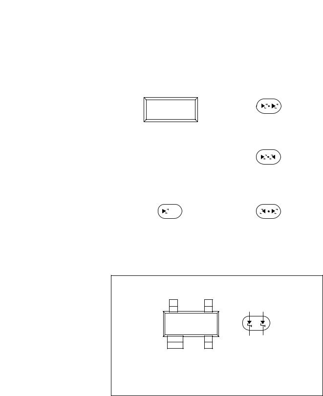
Fig.2 Simplified outline (SOT143B) BAS40-07 and symbol.
1999 Apr 28 |
2 |

Philips Semiconductors |
|
|
Product specification |
|||
|
|
|
|
|
|
|
Schottky barrier (double) diodes |
|
BAS40 series |
||||
|
|
|
|
|
|
|
LIMITING VALUES |
|
|
|
|
|
|
In accordance with the Absolute Maximum Rating System (IEC 134). |
|
|
|
|
||
|
|
|
|
|
|
|
SYMBOL |
PARAMETER |
CONDITIONS |
MIN. |
|
MAX. |
UNIT |
|
|
|
|
|
|
|
Per diode |
|
|
|
|
|
|
|
|
|
|
|
|
|
VR |
continuous reverse voltage |
|
− |
|
40 |
V |
IF |
continuous forward current |
|
− |
|
120 |
mA |
IFRM |
repetitive peak forward current |
tp ≤ 1 s; δ ≤ 0.5 |
− |
|
120 |
mA |
IFSM |
non-repetitive peak forward current |
tp < 10 ms |
− |
|
200 |
mA |
Tstg |
storage temperature |
|
−65 |
|
+150 |
°C |
Tj |
junction temperature |
|
− |
|
150 |
°C |
Tamb |
operating ambient temperature |
|
−65 |
|
+150 |
°C |
ELECTRICAL CHARACTERISTICS
Tamb = 25 °C unless otherwise specified.
SYMBOL |
PARAMETER |
CONDITIONS |
MAX. |
UNIT |
|
|
|
|
|
Per diode |
|
|
|
|
|
|
|
|
|
VF |
forward voltage |
see Fig.3 |
|
|
|
|
IF = 1 mA |
380 |
mV |
|
|
IF = 10 mA |
500 |
mV |
|
|
IF = 40 mA |
1 |
V |
IR |
reverse current |
VR = 30 V; note 1; see Fig.4 |
1 |
μA |
|
|
VR = 40 V; note 1; see Fig.4 |
10 |
μA |
Cd |
diode capacitance |
f = 1 MHz; VR = 0 ; see Fig.6 |
5 |
pF |
Note
1. Pulse test: tp = 300 μs; δ = 0.02.
THERMAL CHARACTERISTICS
SYMBOL |
PARAMETER |
CONDITIONS |
VALUE |
UNIT |
|
|
|
|
|
Rth j-a |
thermal resistance from junction to ambient |
note 1 |
500 |
K/W |
Note |
|
|
|
|
1. Refer to SOT23 or SOT143B standard mounting conditions.
1999 Apr 28 |
3 |
 Loading...