


Philips BC817-40W, BC817-25W, BC818W, BC818-40W, BC818-25W Datasheet
...
DISCRETE SEMICONDUCTORS
DATA SHEET
book, halfpage
M3D102
BC817W
NPN general purpose transistor
Product specification |
|
1999 Apr 15 |
|||||
Supersedes data of 1997 Mar 05 |
|
|
|
|
|
|
|
|
|
|
|
|
|
|
|
|
|
|
|
|
|
|
|
|
|
|
|
|
|
|
|
Philips Semiconductors |
Product specification |
|
|
NPN general purpose transistor |
BC817W |
|
|
|
|
FEATURES
∙High current (max. 500 mA)
∙Low voltage (max. 45 V).
APPLICATIONS
∙ General purpose switching and amplification.
DESCRIPTION
NPN transistor in a SOT323 plastic package. PNP complement: BC807W.
MARKING
TYPE |
MARKING |
TYPE |
MARKING |
NUMBER |
CODE(1) |
NUMBER |
CODE(1) |
BC817W |
6D |
BC818W |
6H |
|
|
|
|
BC817-16W |
6A |
BC818-16W |
6E |
|
|
|
|
BC817-25W |
6B |
BC818-25W |
6F |
|
|
|
|
BC817-40W |
6C |
BC818-40W |
6G |
|
|
|
|
Note
1.= - : Made in Hong Kong.= t : Made in Malaysia.
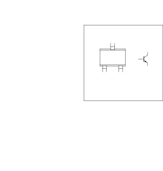
PINNING
PIN |
DESCRIPTION |
|
|
1 |
base |
|
|
2 |
emitter |
|
|
3 |
collector |
|
|
handbook, halfpage |
|
3 |
3
1
2
|
|
1 |
|
2 |
Top view |
|
MAM062 |
||
Fig.1 Simplified outline (SOT323) and symbol.
LIMITING VALUES
In accordance with the Absolute Maximum Rating System (IEC 134).
SYMBOL |
PARAMETER |
CONDITIONS |
MIN. |
MAX. |
UNIT |
|
|
|
|
|
|
VCBO |
collector-base voltage |
open emitter |
− |
50 |
V |
VCEO |
collector-emitter voltage |
open base; IC = 10 mA |
− |
45 |
V |
VEBO |
emitter-base voltage |
open collector |
− |
5 |
V |
IC |
collector current (DC) |
|
− |
500 |
mA |
ICM |
peak collector current |
|
− |
1 |
A |
IBM |
peak base current |
|
− |
200 |
mA |
Ptot |
total power dissipation |
Tamb ≤ 25 °C; note 1 |
− |
200 |
mW |
Tstg |
storage temperature |
|
−65 |
+150 |
°C |
Tj |
junction temperature |
|
− |
150 |
°C |
Tamb |
operating ambient temperature |
|
−65 |
+150 |
°C |
Note
1. Transistor mounted on an FR4 printed-circuit board.
1999 Apr 15 |
2 |

Philips Semiconductors |
|
Product specification |
||
|
|
|
|
|
NPN general purpose transistor |
|
|
BC817W |
|
|
|
|
|
|
THERMAL CHARACTERISTICS |
|
|
|
|
|
|
|
|
|
SYMBOL |
PARAMETER |
CONDITIONS |
VALUE |
UNIT |
|
|
|
|
|
Rth j-a |
thermal resistance from junction to ambient |
note 1 |
625 |
K/W |
Note
1. Transistor mounted on an FR4 printed-circuit board.
CHARACTERISTICS
Tamb = 25 °C unless otherwise specified.
SYMBOL |
PARAMETER |
CONDITIONS |
MIN. |
MAX. |
UNIT |
|
|
|
|
|
|
ICBO |
collector cut-off current |
IE = 0; VCB = 20 V |
− |
100 |
nA |
|
|
IE = 0; VCB = 20 V; Tj = 150 °C |
− |
5 |
μA |
IEBO |
emitter cut-off current |
IC = 0; VEB = 5 V |
− |
100 |
nA |
hFE |
DC current gain |
IC = 100 mA; VCE = 1 V; note 1; |
|
|
|
|
BC817W |
see Figs 2, 3 and 4 |
100 |
600 |
|
|
|
|
|||
|
BC817-16W |
|
100 |
250 |
|
|
BC817-25W |
|
160 |
400 |
|
|
BC817-40W |
|
250 |
600 |
|
|
|
|
|
|
|
|
DC current gain |
IC = 500 mA; VCE = 1 V; note 1 |
40 |
− |
|
VCEsat |
collector-emitter saturation |
IC = 500 mA; IB = 50 mA; note 1 |
− |
700 |
mV |
|
voltage |
|
|
|
|
|
|
|
|
|
|
VBE |
base-emitter voltage |
IC = 500 mA; VCE = 1 V; note 1 |
− |
1.2 |
mV |
Cc |
collector capacitance |
IE = ie = 0; VCB = 10 V; f = 1 MHz |
− |
5 |
pF |
fT |
transition frequency |
IC = 10 mA; VCE = 5 V; f = 100 MHz |
100 |
− |
MHz |
Note
1. Pulse test: tp ≤ 300 μs; δ ≤ 0.02.
1999 Apr 15 |
3 |
 Loading...