


BT136S-800F
Philips BT136S-800F, BT136S-800, BT136S-600G, BT136S-600F, BT136S-500G Datasheet
...
Philips Semiconductors Product specification
Triacs BT136S series
BT136M series
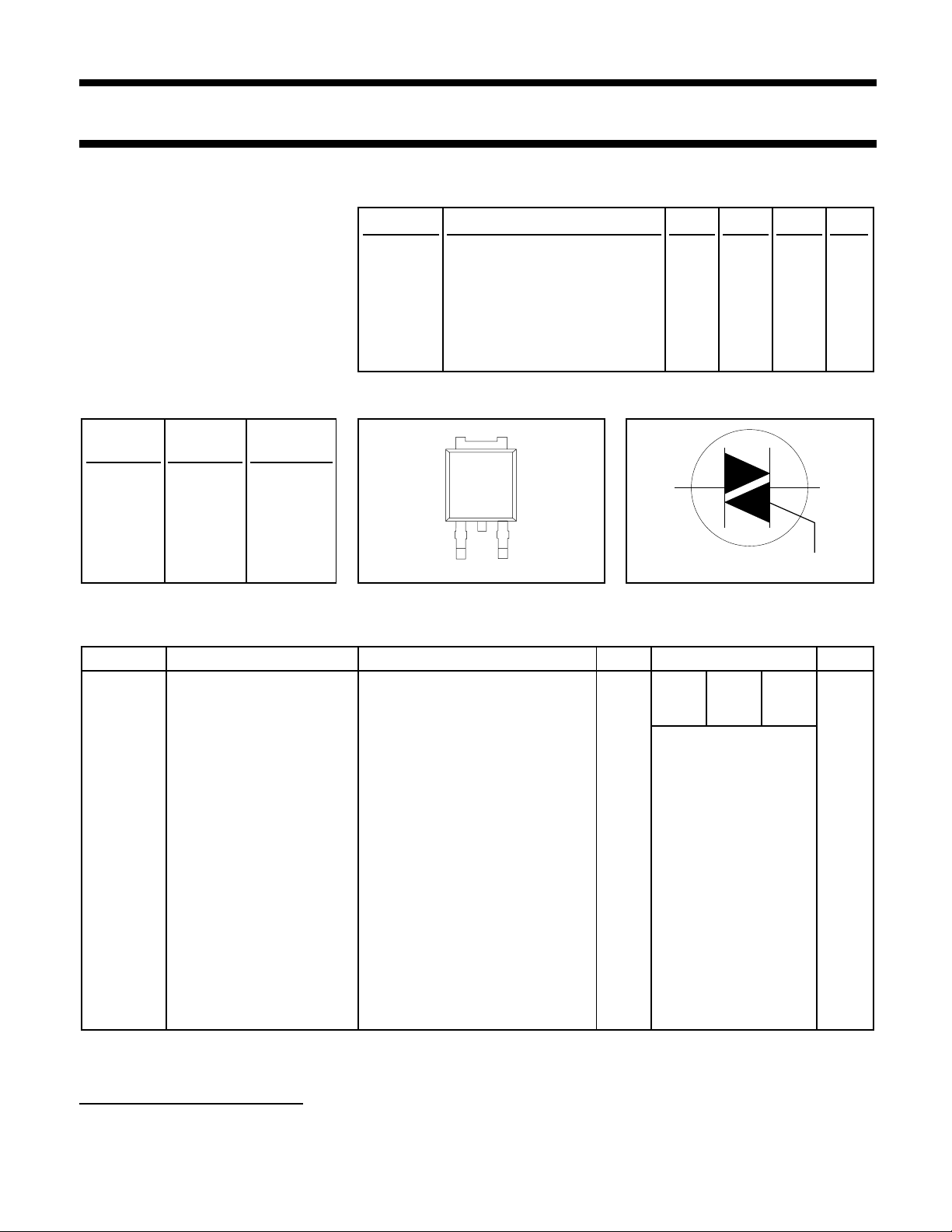
GENERAL DESCRIPTION QUICK REFERENCE DATA
Glass passivated triacs in a plastic SYMBOL PARAMETER MAX. MAX. MAX. UNIT
envelope, suitable for surface
mounting, intended for use in BT136S (or BT136M)- 500 600 800
applications requiring high BT136S (or BT136M)- 500F 600F 800F
bidirectional transient and blocking BT136S (or BT136M)- 500G 600G 800G
voltage capability and high thermal V
DRM
Repetitive peak off-state 500 600 800 V
cycling performance. Typical voltages
applications include motor control, I
T(RMS)
RMS on-state current 4 4 4 A
industrial and domestic lighting, I
TSM
Non-repetitive peak on-state 25 25 25 A
heating and static switching. current
PINNING - SOT428 PIN CONFIGURATION SYMBOL
PIN Standard Alternative
NUMBER S M
1 MT1 gate
2 MT2 MT2
3 gate MT1
tab MT2 MT2
LIMITING VALUES
Limiting values in accordance with the Absolute Maximum System (IEC 134).
SYMBOL PARAMETER CONDITIONS MIN. MAX. UNIT
-500 -600 -800
V
DRM
Repetitive peak off-state - 500
1
600
1
800 V
voltages
I
T(RMS)
RMS on-state current full sine wave; T
mb
≤ 107 ˚C - 4 A
I
TSM
Non-repetitive peak full sine wave; T
j
= 25 ˚C prior to
on-state current surge
t = 20 ms - 25 A
t = 16.7 ms - 27 A
I
2
tI
2
t for fusing t = 10 ms - 3.1 A
2
s
dI
T
/dt Repetitive rate of rise of I
TM
= 6 A; I
G
= 0.2 A;
on-state current after dI
G
/dt = 0.2 A/µs
triggering T2+ G+ - 50 A/µs
T2+ G- - 50 A/µs
T2- G- - 50 A/µs
T2- G+ - 10 A/µs
I
GM
Peak gate current - 2 A
V
GM
Peak gate voltage - 5 V
P
GM
Peak gate power - 5 W
P
G(AV)
Average gate power over any 20 ms period - 0.5 W
T
stg
Storage temperature -40 150 ˚C
T
j
Operating junction - 125 ˚C
temperature
1
2
3
tab
T1T2
G
1 Although not recommended, off-state voltages up to 800V may be applied without damage, but the triac may
switch to the on-state. The rate of rise of current should not exceed 3 A/µs.
October 1997 1 Rev 1.100

Philips Semiconductors Product specification
Triacs BT136S series
BT136M series
THERMAL RESISTANCES
SYMBOL PARAMETER CONDITIONS MIN. TYP. MAX. UNIT
R
th j-mb
Thermal resistance full cycle - - 3.0 K/W
junction to mounting base half cycle - - 3.7 K/W
R
th j-a
Thermal resistance pcb (FR4) mounted; footprint as in Fig.14 - 75 - K/W
junction to ambient
STATIC CHARACTERISTICS
T
j
= 25 ˚C unless otherwise stated
SYMBOL PARAMETER CONDITIONS MIN. TYP. MAX. UNIT
BT136S- ... ...F ...G
I
GT
Gate trigger current V
D
= 12 V; I
T
= 0.1 A
T2+ G+ - 5 35 25 50 mA
T2+ G- - 8 35 25 50 mA
T2- G- - 11 35 25 50 mA
T2- G+ - 30 70 70 100 mA
I
L
Latching current V
D
= 12 V; I
GT
= 0.1 A
T2+ G+ - 7 20 20 30 mA
T2+ G- - 16 30 30 45 mA
T2- G- - 5 20 20 30 mA
T2- G+ - 7 30 30 45 mA
I
H
Holding current V
D
= 12 V; I
GT
= 0.1 A - 5 15 15 30 mA
V
T
On-state voltage I
T
= 5 A - 1.4 1.70 V
V
GT
Gate trigger voltage V
D
= 12 V; I
T
= 0.1 A - 0.7 1.5 V
V
D
= 400 V; I
T
= 0.1 A; 0.25 0.4 - V
T
j
= 125 ˚C
I
D
Off-state leakage current V
D
= V
DRM(max)
; - 0.1 0.5 mA
T
j
= 125 ˚C
DYNAMIC CHARACTERISTICS
T
j
= 25 ˚C unless otherwise stated
SYMBOL PARAMETER CONDITIONS MIN. TYP. MAX. UNIT
BT136S (or BT136M)- ... ...F ...G
dV
D
/dt Critical rate of rise of V
DM
= 67% V
DRM(max)
; 100 50 200 250 - V/µs
off-state voltage T
j
= 125 ˚C; exponential
waveform; gate open
circuit
dV
com
/dt Critical rate of change of V
DM
= 400 V; T
j
= 95 ˚C; - - 10 50 - V/µs
commutating voltage I
T(RMS)
= 4 A;
dI
com
/dt = 1.8 A/ms; gate
open circuit
t
gt
Gate controlled turn-on I
TM
= 6 A; V
D
= V
DRM(max)
;- - - 2 -µs
time I
G
= 0.1 A; dI
G
/dt = 5 A/µs
October 1997 2 Rev 1.100
 Loading...