MOTOROLA MC74ACT245ML1, MC74ACT245ML2, MC74ACT245MR1, MC74ACT245MR2, MC74ACT245DTR2 Datasheet
...
Octal Bidirectional Transceiver with 3 State Inputs/Outputs
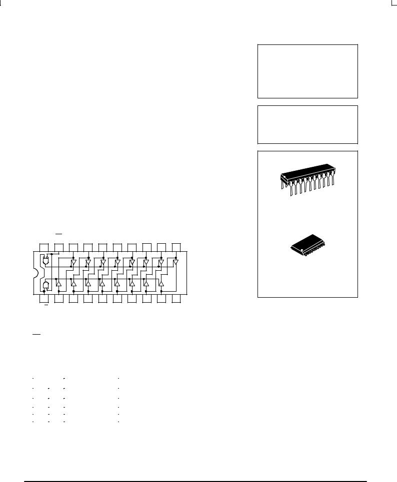
The MC74AC245/74ACT245 contains eight non-inverting bidirectional buffers with 3-state outputs and is intended for bus-oriented applications. Current sinking capability is 24 mA at both the A and B ports. The Transmit/Receive (T/R) input determines the direction of data flow through the bidirectional transceiver. Transmit (active-HIGH) enables data from A ports to B ports; Receive (active-LOW) enables data from B ports to A ports. The Output Enable input, when HIGH, disables both A and B ports by placing them in a High Z condition.
•Noninverting Buffers
•Bidirectional Data Path
•A and B Outputs Source/Sink 24 mA
•′ACT245 Has TTL Compatible Inputs
VCC |
OE |
B0 |
B1 |
B2 |
B3 |
B4 |
B5 |
B6 |
B7 |
20 |
19 |
18 |
17 |
16 |
15 |
14 |
13 |
12 |
11 |
1 |
2 |
3 |
4 |
5 |
6 |
7 |
8 |
9 |
10 |
T/R |
A0 |
A1 |
A2 |
A3 |
A4 |
A5 |
A6 |
A7 |
GND |
PIN NAMES
OE |
Output Enable Input |
T/R |
Transmit/Receive Input |
A0±A7 |
Side A 3-State Inputs or 3-State Outputs |
B0±B7 |
Side B 3-State Inputs or 3-State Outputs |
TRUTH TABLES
Inputs |
Outputs |
||
|
|
|
|
OE |
|
T/R |
|
|
|
||
|
|
|
|
L |
|
L |
Bus B Data to Bus A |
L |
|
H |
Bus A Data to Bus B |
H |
|
X |
High Z State |
|
|
|
|
H = HIGH Voltage Level
L = LOW Voltage Level
X = Immaterial
MC74AC245
MC74ACT245
OCTAL BIDIRECTIONAL
TRANSCEIVER
WITH 3-STATE
INPUTS/OUTPUTS
N SUFFIX
CASE 738-03
PLASTIC
DW SUFFIX
CASE 751D-04
PLASTIC
FACT DATA
5-1

MC74AC245 MC74ACT245
MAXIMUM RATINGS*
Symbol |
Parameter |
Value |
Unit |
|
|
|
|
VCC |
DC Supply Voltage (Referenced to GND) |
±0.5 to +7.0 |
V |
Vin |
DC Input Voltage (Referenced to GND) |
±0.5 to VCC +0.5 |
V |
Vout |
DC Output Voltage (Referenced to GND) |
±0.5 to VCC +0.5 |
V |
Iin |
DC Input Current, per Pin |
±20 |
mA |
Iout |
DC Output Sink/Source Current, per Pin |
±50 |
mA |
ICC |
DC VCC or GND Current per Output Pin |
±50 |
mA |
Tstg |
Storage Temperature |
±65 to +150 |
°C |
*Maximum Ratings are those values beyond which damage to the device may occur. Functional operation should be restricted to the Recommended Operating Conditions.
RECOMMENDED OPERATING CONDITIONS
Symbol |
Parameter |
|
Min |
Typ |
Max |
Unit |
|
|
|
|
|
|
|
|
|
VCC |
Supply Voltage |
′AC |
2.0 |
5.0 |
6.0 |
V |
|
|
|
|
|
||||
′ACT |
4.5 |
5.0 |
5.5 |
||||
|
|
|
|||||
|
|
|
|
|
|
|
|
Vin, Vout |
DC Input Voltage, Output Voltage (Ref. to GND) |
|
0 |
|
VCC |
V |
|
|
Input Rise and Fall Time (Note 1) |
VCC @ 3.0 V |
|
150 |
|
|
|
tr, tf |
VCC @ 4.5 V |
|
40 |
|
ns/V |
||
′AC Devices except Schmitt Inputs |
|
|
|||||
|
|
VCC @ 5.5 V |
|
25 |
|
|
|
tr, tf |
Input Rise and Fall Time (Note 2) |
VCC @ 4.5 V |
|
10 |
|
ns/V |
|
′ACT Devices except Schmitt Inputs |
VCC @ 5.5 V |
|
8.0 |
|
|||
|
|
|
|
|
|||
TJ |
Junction Temperature (PDIP) |
|
|
|
140 |
°C |
|
TA |
Operating Ambient Temperature Range |
|
±40 |
25 |
85 |
°C |
|
IOH |
Output Current Ð High |
|
|
|
±24 |
mA |
|
IOL |
Output Current Ð Low |
|
|
|
24 |
mA |
1.Vin from 30% to 70% VCC; see individual Data Sheets for devices that differ from the typical input rise and fall times.
2.Vin from 0.8 V to 2.0 V; see individual Data Sheets for devices that differ from the typical input rise and fall times.
FACT DATA
5-2
 Loading...