


Motorola MC68L11KA1FN3, MC68L11KA1FU1, MC68L11KA1FU3, MC68L11KA2FN1, MC68L11KA0FU3 Datasheet
...MOTOROLA
SEMICONDUCTOR
TECHNICAL DATA
Order this document by MC68HC11KA4TS/D
M68HC11 KA Series
Technical Summary
8-Bit Microcontroller
1 Introduction
The MC68HC11KA4 family of microcontrollers are enhanced derivatives of the MC68HC11F1 and, as shown in the block diagram, include many additional features. The family includes the MC68HC11KA0, MC68HC11KA1, MC68HC11KA3, MC68HC11KA4, MC68HC711KA4, MC68HC11KA2, and the MC68HC711KA2. These MCUs, with a non-multiplexed expanded bus, are characterized by high speed and low power consumption. The fully static design allows operation at frequencies from 4 MHz to dc.
This technical summary contains information concerning standard, custom-ROM, and extended-volt- age devices. Standard devices are those with disabled ROM (MC68HC11KA1), disabled EEPROM (MC68HC11KA0), and EPROM replacing ROM (MC68HC711KA4). The MC68HC11KA2 and MC68HC711KA2 contain 32 Kbytes of ROM/EPROM instead of 24 Kbytes. Custom-ROM devices have a ROM array that is programmed at the factory to customer specifications. Extended-voltage devices are guaranteed to operate over a much greater voltage range (3.0 Vdc to 5.5 Vdc) at lower frequencies than the standard devices. Refer to the ordering information on the following pages.
In this summary, ROM/EPROM refers to ROM for ROM-based devices and refers to EPROM for EPROM-based devices.
1.1Features
•M68HC11 Central Processing Unit (CPU)
•Power Saving STOP and WAIT Modes
•768 Bytes RAM in MC68HC11KA4, 1024 Bytes RAM in MC68HC11KA2 (Saved During Standby)
•640 Bytes Electrically Erasable Programmable ROM (EEPROM)
•24 Kbytes ROM/EPROM, 32 Kbytes ROM/EPROM in MC68HC11KA2
•PROG Mode Allows Use of Standard EPROM Programmer (27256 Footprint)
•Non-multiplexed Address and Data Buses
•Enhanced 16-Bit Timer with Four-Stage Programmable Prescaler
—Three Input Capture (IC) Channels
—Four Output Compare (OC) Channels
—One Additional Channel, Selectable as Fourth IC or Fifth OC
•8-Bit Pulse Accumulator
•Four 8-Bit or Two 16-Bit Pulse-Width Modulation (PWM) Timer Channels
•Real-Time Interrupt Circuit
•Computer Operating Properly (COP) Watchdog
•Enhanced Asynchronous Nonreturn to Zero (NRZ) Serial Communications Interface (SCI)
•Enhanced Synchronous Serial Peripheral Interface (SPI)
•Eight-Channel 8-Bit Analog-to-Digital (A/D) Converter (Four Channels on 64-Pin Version)
•Seven Bidirectional Input/Output (I/O) Ports (43 Pins)
•One Fixed Input-Only Port (8 Pins, 4 Pins on 64-Pin Version)
•Available in 68-Pin Plastic Leaded Chip Carrier (Custom ROM/OTPROM), 68-Pin Windowed Ceramic Leaded Chip Carrier (EPROM), or 64-Pin Quad Flat Pack (Custom ROM/OTPROM)
This document contains information on a new product. Specifications and information herein are subject to change without notice.
© MOTOROLA INC., 1996

Table 1 Standard Device Ordering Information
Package |
Temperature |
CONFIG |
Description |
Frequency |
MC Order Number |
|
|
|
|
|
|
68-Pin Plastic |
–40°το + 85°C |
$DF |
BUFFALO ROM |
4 MHz |
MC68HC11KA4BCFN4 |
Leaded Chip |
|
|
|
|
|
–40°to + 85°C |
$DD |
No ROM |
2 MHz |
MC68HC11KA1CFN2 |
|
Carrier |
|
|
|
|
|
|
|
|
3 MHz |
MC68HC11KA1CFN3 |
|
|
|
|
|
||
|
|
|
|
|
|
|
|
|
|
4 MHz |
MC68HC11KA1CFN4 |
|
|
|
|
|
|
|
–40°to + 105°C |
$DD |
No ROM |
2 MHz |
MC68HC11KA1VFN2 |
|
|
|
|
|
|
|
|
|
|
3 MHz |
MC68HC11KA1VFN3 |
|
|
|
|
|
|
|
|
|
|
4 MHz |
MC68HC11KA1VFN4 |
|
|
|
|
|
|
|
–40°to + 125°C |
$DD |
No ROM |
2 MHz |
MC68HC11KA1MFN2 |
|
|
|
|
|
|
|
|
|
|
3 MHz |
MC68HC11KA1MFN3 |
|
|
|
|
|
|
|
|
|
|
4 MHz |
MC68HC11KA1MFN4 |
|
|
|
|
|
|
|
–40°to + 85°C |
$DC |
No ROM, No EEPROM |
2 MHz |
MC68HC11KA0CFN2 |
|
|
|
|
|
|
|
|
|
|
3 MHz |
MC68HC11KA0CFN3 |
|
|
|
|
|
|
|
|
|
|
4 MHz |
MC68HC11KA0CFN4 |
|
|
|
|
|
|
|
–40°to + 105°C |
$DC |
No ROM, No EEPROM |
2 MHz |
MC68HC11KA0VFN2 |
|
|
|
|
|
|
|
|
|
|
3 MHz |
MC68HC11KA0VFN3 |
|
|
|
|
|
|
|
|
|
|
4 MHz |
MC68HC11KA0VFN4 |
|
|
|
|
|
|
|
–40°to + 125°C |
$DC |
No ROM, No EEPROM |
2 MHz |
MC68HC11KA0MFN2 |
|
|
|
|
|
|
|
|
|
|
3 MHz |
MC68HC11KA0MFN3 |
|
|
|
|
|
|
|
|
|
|
4 MHz |
MC68HC11KA0MFN4 |
|
|
|
|
|
|
|
–40°to + 85°C |
$DF |
24 Kbytes OTPROM |
2 MHz |
MC68HC711KA4CFN2 |
|
|
|
|
|
|
|
|
|
|
3 MHz |
MC68HC711KA4CFN3 |
|
|
|
|
|
|
|
|
|
|
4 MHz |
MC68HC711KA4CFN4 |
|
|
|
|
|
|
|
–40°to + 105°C |
$DF |
24 Kbytes OTPROM |
2 MHz |
MC68HC711KA4VFN2 |
|
|
|
|
|
|
|
|
|
|
3 MHz |
MC68HC711KA4VFN3 |
|
|
|
|
|
|
|
|
|
|
4 MHz |
MC68HC711KA4VFN4 |
|
|
|
|
|
|
|
–40°to + 125°C |
$DF |
24 Kbytes OTPROM |
2 MHz |
MC68HC711KA4MFN2 |
|
|
|
|
|
|
|
|
|
|
3 MHz |
MC68HC711KA4MFN3 |
|
|
|
|
|
|
|
|
|
|
4 MHz |
MC68HC711KA4MFN4 |
|
|
|
|
|
|
|
–40°to + 85°C |
$DF |
32 Kbytes OTPROM |
2 MHz |
MC68HC711KA2CFN2 |
|
|
|
|
|
|
|
|
|
|
3 MHz |
MC68HC711KA2CFN3 |
|
|
|
|
|
|
|
|
|
|
4 MHz |
MC68HC711KA2CFN4 |
|
|
|
|
|
|
|
–40°to + 105°C |
$DF |
32 Kbytes OTPROM |
2 MHz |
MC68HC711KA2VFN2 |
|
|
|
|
|
|
|
|
|
|
3 MHz |
MC68HC711KA2VFN3 |
|
|
|
|
|
|
|
|
|
|
4 MHz |
MC68HC711KA2VFN4 |
|
|
|
|
|
|
|
–40°to + 125°C |
$DF |
32 Kbytes OTPROM |
2 MHz |
MC68HC711KA2MFN2 |
|
|
|
|
|
|
|
|
|
|
3 MHz |
MC68HC711KA2MFN3 |
|
|
|
|
|
|
|
|
|
|
4 MHz |
MC68HC711KA2MFN4 |
|
|
|
|
|
|
MOTOROLA |
MC68HC11KA4 |
2 |
MC68HC11KA4TS/D |

Table 1 Standard Device Ordering Information (Continued)
Package |
Temperature |
CONFIG |
Description |
Frequency |
MC Order Number |
|
|
|
|
|
|
64-Pin Quad |
–40°to + 85°C |
$DF |
BUFFALO ROM |
4 MHz |
MC68HC11KA4BCFU4 |
Flat Pack |
|
|
|
|
|
–40°to + 85°C |
$DF |
24 Kbytes OTPROM |
2 MHz |
MC68HC711KA4CFU2 |
|
|
|
|
|
|
|
|
|
|
|
3 MHz |
MC68HC711KA4CFU3 |
|
|
|
|
|
|
|
|
|
|
4 MHz |
MC68HC711KA4CFU4 |
|
|
|
|
|
|
|
–40°to + 105°C |
$DF |
24 Kbytes OTPROM |
2 MHz |
MC68HC711KA4VFU2 |
|
|
|
|
|
|
|
|
|
|
3 MHz |
MC68HC711KA4VFU3 |
|
|
|
|
|
|
|
|
|
|
4 MHz |
MC68HC711KA4VFU4 |
|
|
|
|
|
|
|
–40°to + 125°C |
$DF |
24 Kbytes OTPROM |
2 MHz |
MC68HC711KA4MFU2 |
|
|
|
|
|
|
|
|
|
|
3 MHz |
MC68HC711KA4MFU3 |
|
|
|
|
|
|
|
|
|
|
4 MHz |
MC68HC711KA4MFU4 |
|
|
|
|
|
|
|
–40°to + 85°C |
$DF |
32 Kbytes OTPROM |
2 MHz |
MC68HC711KA2CFU2 |
|
|
|
|
|
|
|
|
|
|
3 MHz |
MC68HC711KA2CFU3 |
|
|
|
|
|
|
|
|
|
|
4 MHz |
MC68HC711KA2CFU4 |
|
|
|
|
|
|
|
–40°to + 105°C |
$DF |
32 Kbytes OTPROM |
2 MHz |
MC68HC711KA2VFU2 |
|
|
|
|
|
|
|
|
|
|
3 MHz |
MC68HC711KA2VFU3 |
|
|
|
|
|
|
|
|
|
|
4 MHz |
MC68HC711KA2VFU4 |
|
|
|
|
|
|
|
–40°to + 125°C |
$DF |
32 Kbytes OTPROM |
2 MHz |
MC68HC711KA2MFU2 |
|
|
|
|
|
|
|
|
|
|
3 MHz |
MC68HC711KA2MFU3 |
|
|
|
|
|
|
|
|
|
|
4 MHz |
MC68HC711KA2MFU4 |
|
|
|
|
|
|
|
–40°to + 85°C |
$DD |
No ROM |
2 MHz |
MC68HC11KA1CFU2 |
|
|
|
|
|
|
|
|
|
|
3 MHz |
MC68HC11KA1CFU3 |
|
|
|
|
|
|
|
|
|
|
4 MHz |
MC68HC11KA1CFU4 |
|
|
|
|
|
|
|
–40°to + 105°C |
$DD |
No ROM |
2 MHz |
MC68HC11KA1VFU2 |
|
|
|
|
|
|
|
|
|
|
3 MHz |
MC68HC11KA1VFU3 |
|
|
|
|
|
|
|
|
|
|
4 MHz |
MC68HC11KA1VFU4 |
|
|
|
|
|
|
|
–40°to + 85°C |
$DC |
No ROM, No EEPROM |
2 MHz |
MC68HC11KA0CFU2 |
|
|
|
|
|
|
|
|
|
|
3 MHz |
MC68HC11KA0CFU3 |
|
|
|
|
|
|
|
|
|
|
4 MHz |
MC68HC11KA0CFU4 |
|
|
|
|
|
|
|
–40°to + 105°C |
$DC |
No ROM, No EEPROM |
2 MHz |
MC68HC11KA0VFU2 |
|
|
|
|
|
|
|
|
|
|
3 MHz |
MC68HC11KA0VFU3 |
|
|
|
|
|
|
|
|
|
|
4 MHz |
MC68HC11KA0VFU4 |
|
|
|
|
|
|
MC68HC11KA4 |
MOTOROLA |
MC68HC11KA4TS/D |
3 |

Table 1 Standard Device Ordering Information (Continued)
Package |
Temperature |
CONFIG |
Description |
Frequency |
MC Order Number |
|
|
|
|
|
|
68-Pin Cerquad |
–40°to + 85°C |
$DF |
24 Kbytes EPROM |
2 MHz |
MC68HC711KA4CFS2 |
|
|
|
|
|
|
|
|
|
|
3 MHz |
MC68HC711KA4CFS3 |
|
|
|
|
|
|
|
|
|
|
4 MHz |
MC68HC711KA4CFS4 |
|
|
|
|
|
|
|
–40°to + 105°C |
$DF |
24 Kbytes EPROM |
2 MHz |
MC68HC711KA4VFS2 |
|
|
|
|
|
|
|
|
|
|
3 MHz |
MC68HC711KA4VFS3 |
|
|
|
|
|
|
|
|
|
|
4 MHz |
MC68HC711KA4VFS4 |
|
|
|
|
|
|
|
–40°to + 125°C |
$DF |
24 Kbytes EPROM |
2 MHz |
MC68HC711KA4MFS2 |
|
|
|
|
|
|
|
|
|
|
3 MHz |
MC68HC711KA4MFS3 |
|
|
|
|
|
|
|
|
|
|
4 MHz |
MC68HC711KA4MFS4 |
|
|
|
|
|
|
|
–40°to + 85°C |
$DF |
32 Kbytes EPROM |
2 MHz |
MC68HC711KA2CFS2 |
|
|
|
|
|
|
|
|
|
|
3 MHz |
MC68HC711KA2CFS3 |
|
|
|
|
|
|
|
|
|
|
4 MHz |
MC68HC711KA2CFS4 |
|
|
|
|
|
|
|
–40°to + 105°C |
$DF |
32 Kbytes EPROM |
2 MHz |
MC68HC711KA2VFS2 |
|
|
|
|
|
|
|
|
|
|
3 MHz |
MC68HC711KA2VFS3 |
|
|
|
|
|
|
|
|
|
|
4 MHz |
MC68HC711KA2VFS4 |
|
|
|
|
|
|
|
–40°to + 125°C |
$DF |
32 Kbytes EPROM |
2 MHz |
MC68HC711KA2MFS2 |
|
|
|
|
|
|
|
|
|
|
3 MHz |
MC68HC711KA2MFS3 |
|
|
|
|
|
|
|
|
|
|
4 MHz |
MC68HC711KA2MFS4 |
|
|
|
|
|
|
MOTOROLA |
MC68HC11KA4 |
4 |
MC68HC11KA4TS/D |

Table 2 Custom ROM Device Ordering Information
Package |
Temperature |
Description |
Frequency |
MC Order Number |
|
|
|
|
|
68-Pin Plastic |
–40°to + 85°C |
24 Kbytes Custom ROM |
2 MHz |
MC68HC11KA4CFN2 |
Leaded Chip |
|
|
|
|
|
|
3 MHz |
MC68HC11KA4CFN3 |
|
Carrier |
|
|
||
|
|
|
|
|
|
|
4 MHz |
MC68HC11KA4CFN4 |
|
|
|
|
||
|
|
|
|
|
|
–40°to + 105°C |
24 Kbytes Custom ROM |
2 MHz |
MC68HC11KA4VFN2 |
|
|
|
|
|
|
|
|
3 MHz |
MC68HC11KA4VFN3 |
|
|
|
|
|
|
|
|
4 MHz |
MC68HC11KA4VFN4 |
|
|
|
|
|
|
–40°to + 125°C |
24 Kbytes Custom ROM |
2 MHz |
MC68HC11KA4MFN2 |
|
|
|
|
|
|
|
|
3 MHz |
MC68HC11KA4MFN3 |
|
|
|
|
|
|
|
|
4 MHz |
MC68HC11KA4MFN4 |
|
|
|
|
|
|
–40°to + 85°C |
32 Kbytes Custom ROM |
2 MHz |
MC68HC11KA2CFN2 |
|
|
|
|
|
|
|
|
3 MHz |
MC68HC11KA2CFN3 |
|
|
|
|
|
|
|
|
4 MHz |
MC68HC11KA2CFN4 |
|
|
|
|
|
|
–40°to + 105°C |
32 Kbytes Custom ROM |
2 MHz |
MC68HC11KA2VFN2 |
|
|
|
|
|
|
|
|
3 MHz |
MC68HC11KA2VFN3 |
|
|
|
|
|
|
|
|
4 MHz |
MC68HC11KA2VFN4 |
|
|
|
|
|
|
–40°to + 125°C |
32 Kbytes Custom ROM |
2 MHz |
MC68HC11KA2MFN2 |
|
|
|
|
|
|
|
|
3 MHz |
MC68HC11KA2MFN3 |
|
|
|
|
|
|
|
|
4 MHz |
MC68HC11KA2MFN4 |
|
|
|
|
|
|
–40°to + 85°C |
24 Kbytes Custom ROM, |
2 MHz |
MC68HC11KA3CFN2 |
|
|
|
|
|
|
|
No EEPROM |
3 MHz |
MC68HC11KA3CFN3 |
|
|
|
|
|
|
|
|
4 MHz |
MC68HC11KA3CFN4 |
|
|
|
|
|
|
–40°to + 105°C |
24 Kbytes Custom ROM, |
2 MHz |
MC68HC11KA3VFN2 |
|
|
|
|
|
|
|
No EEPROM |
3 MHz |
MC68HC11KA3VFN3 |
|
|
|
|
|
|
|
|
4 MHz |
MC68HC11KA3VFN4 |
|
|
|
|
|
|
–40°to + 125°C |
24 Kbytes Custom ROM, |
2 MHz |
MC68HC11KA3MFN2 |
|
|
|
|
|
|
|
No EEPROM |
3 MHz |
MC68HC11KA3MFN3 |
|
|
|
|
|
|
|
|
4 MHz |
MC68HC11KA3MFN4 |
|
|
|
|
|
MC68HC11KA4 |
MOTOROLA |
MC68HC11KA4TS/D |
5 |

Table 2 Custom ROM Device Ordering Information (Continued)
Package |
Temperature |
Description |
Frequency |
MC Order Number |
|
|
|
|
|
64-Pin Quad |
–40°to + 85°C |
24 Kbytes Custom ROM |
2 MHz |
MC68HC11KA4CFU2 |
Flat Pack |
|
|
|
|
|
|
3 MHz |
MC68HC11KA4CFU3 |
|
|
|
|
||
|
|
|
|
|
|
|
|
4 MHz |
MC68HC11KA4CFU4 |
|
|
|
|
|
|
–40°to + 105°C |
24 Kbytes Custom ROM |
2 MHz |
MC68HC11KA4VFU2 |
|
|
|
|
|
|
|
|
3 MHz |
MC68HC11KA4VFU3 |
|
|
|
|
|
|
|
|
4 MHz |
MC68HC11KA4VFU4 |
|
|
|
|
|
|
–40°to + 85°C |
32 Kbytes Custom ROM |
2 MHz |
MC68HC11KA2CFU2 |
|
|
|
|
|
|
|
|
3 MHz |
MC68HC11KA2CFU3 |
|
|
|
|
|
|
|
|
4 MHz |
MC68HC11KA2CFU4 |
|
|
|
|
|
|
–40°to + 105°C |
32 Kbytes Custom ROM |
2 MHz |
MC68HC11KA2VFU2 |
|
|
|
|
|
|
|
|
3 MHz |
MC68HC11KA2VFU3 |
|
|
|
|
|
|
|
|
4 MHz |
MC68HC11KA2VFU4 |
|
|
|
|
|
|
–40°to + 85°C |
24 Kbytes Custom ROM, |
2 MHz |
MC68HC11KA3CFU2 |
|
|
|
|
|
|
|
No EEPROM |
3 MHz |
MC68HC11KA3CFU3 |
|
|
|
|
|
|
|
|
4 MHz |
MC68HC11KA3CFU4 |
|
|
|
|
|
|
–40°to + 105°C |
24 Kbytes Custom ROM, |
2 MHz |
MC68HC11KA3VFU2 |
|
|
|
|
|
|
|
No EEPROM |
3 MHz |
MC68HC11KA3VFU3 |
|
|
|
|
|
|
|
|
4 MHz |
MC68HC11KA3VFU4 |
|
|
|
|
|
Table 3 Extended Voltage (3.0 Vdc to 5.5 Vdc) Device Ordering Information
Package |
Temperature |
Description |
Frequency |
MC Order Number |
|
|
|
|
|
68-Pin Plastic |
–20°to + 70°C |
24 Kbytes Custom ROM |
1 MHz |
MC68L11KA4FN1 |
Leaded Chip |
|
|
|
|
|
|
3 MHz |
MC68L11KA4FN3 |
|
Carrier |
|
|
||
|
|
|
|
|
|
32 Kbytes Custom ROM |
1 MHz |
MC68L11KA2FN1 |
|
|
|
|||
|
|
|
|
|
|
|
|
3 MHz |
MC68L11KA2FN3 |
|
|
|
|
|
|
|
No ROM |
1 MHz |
MC68L11KA1FN1 |
|
|
|
|
|
|
|
|
3 MHz |
MC68L11KA1FN3 |
|
|
|
|
|
|
|
No ROM, No EEPROM |
1 MHz |
MC68L11KA0FN1 |
|
|
|
|
|
|
|
|
3 MHz |
MC68L11KA0FN3 |
|
|
|
|
|
|
|
24 Kbytes Custom ROM, |
1 MHz |
MC68L11KA3FN1 |
|
|
|
|
|
|
|
No EEPROM |
3 MHz |
MC68L11KA3FN3 |
|
|
|
|
|
64-Pin Quad |
–20°to + 70°C |
24 Kbytes Custom ROM |
1 MHz |
MC68L11KA4FU1 |
Flat Pack |
|
|
|
|
|
|
3 MHz |
MC68L11KA4FU3 |
|
|
|
|
||
|
|
|
|
|
|
|
32 Kbytes Custom ROM |
1 MHz |
MC68L11KA2FU1 |
|
|
|
|
|
|
|
|
3 MHz |
MC68L11KA2FU3 |
|
|
|
|
|
|
|
No ROM |
1 MHz |
MC68L11KA1FU1 |
|
|
|
|
|
|
|
|
3 MHz |
MC68L11KA1FU3 |
|
|
|
|
|
|
|
No ROM, No EEPROM |
1 MHz |
MC68L11KA0FU1 |
|
|
|
|
|
|
|
|
3 MHz |
MC68L11KA0FU3 |
|
|
|
|
|
|
|
24 Kbytes Custom ROM, |
1 MHz |
MC68L11KA3FU1 |
|
|
|
|
|
|
|
No EEPROM |
3 MHz |
MC68L11KA3FU3 |
|
|
|
|
|
MOTOROLA |
MC68HC11KA4 |
6 |
MC68HC11KA4TS/D |

PA0/IC3 |
PA1/IC2 |
PA2/IC1 |
PA3/OC5/IC4/OC1 |
PA4/OC4/OC1 |
PA5/OC3/OC1 |
PA6/OC2/OC1 |
PA7/PAI/OC1 |
V |
V |
V |
PD5/SS |
PD4/SCK |
PD3/MOSI |
PD2/MISO |
PD1/TxD |
PD0/RxD |
|
|
|
|
|
|
|
|
INT |
EXT |
EXT |
|
|
|
|
|
|
|
|
|
|
|
|
|
|
DD |
DD |
SS |
|
|
|
|
|
|
9 |
8 |
7 |
6 |
5 |
4 |
3 |
2 |
|
68 |
67 |
66 |
65 |
64 |
63 |
62 |
61 |
PB7/ADDR15 |
10 |
||||||
PB6/ADDR14 |
11 |
||||||
PB5/ADDR13 |
12 |
||||||
PB4/ADDR12 |
13 |
||||||
PB3/ADDR11 |
14 |
||||||
PB2/ADDR10 |
15 |
||||||
|
PB1/ADDR9 |
16 |
|||||
|
PB0/ADDR8 |
17 |
|||||
|
PH0/PW1 |
18 |
|||||
|
PH1/PW2 |
19 |
|||||
|
PH2/PW3 |
20 |
|||||
|
PH3/PW4 |
21 |
|||||
|
|
|
|
|
22 |
||
|
XIRQ/VPPE* |
||||||
|
PG7/R/W |
|
|
23 |
|||
|
|
|
|
|
|
|
24 |
|
|
|
IRQ |
||||
|
|
AVDD |
25 |
||||
|
PE7/AN7 |
26 |
|||||
27 |
28 |
PE6/AN6 |
PE5/AN5 |
* VPPE
|
|
|
|
|
|
|
|
|
|
|
|
|
|
60 |
|
|
|
|
|
|
|
|
|
1 |
|
|
|
|
|
|
|
MODA/LIR |
|||
|
|
|
|
|
|
|
|
|
|
|
|
|
|
59 |
MODB/VSTBY |
||
|
|
|
|
|
|
|
|
|
|
|
|
|
|
58 |
RESET |
|
|
|
|
|
|
|
|
|
|
|
|
|
|
|
|
57 |
XTAL |
||
|
|
|
|
|
|
|
|
|
|
|
|
|
|
56 |
EXTAL |
||
|
|
|
|
|
|
|
|
|
|
|
|
|
|
55 |
XOUT |
||
|
|
|
|
|
|
|
|
|
|
|
|
|
|
54 |
E |
||
|
|
|
|
MC68HC(7)11KA4 |
|
|
|
|
|
53 |
PC7/DATA7 |
||||||
|
|
|
|
|
|
|
|
|
52 |
PC6/DATA6 |
|||||||
|
|
|
|
MC68HC(7)11KA2 |
|
|
|
|
|
||||||||
|
|
|
|
|
|
|
|
|
51 |
PC5/DATA5 |
|||||||
|
|
|
|
|
|
|
|
|
|
|
|
|
|
||||
|
|
|
|
|
|
|
|
|
|
|
|
|
|
50 |
PC4/DATA4 |
||
|
|
|
|
|
|
|
|
|
|
|
|
|
|
49 |
PC3/DATA3 |
||
|
|
|
|
|
|
|
|
|
|
|
|
|
|
48 |
PC2/DATA2 |
||
|
|
|
|
|
|
|
|
|
|
|
|
|
|
47 |
PC1/DATA1 |
||
|
|
|
|
|
|
|
|
|
|
|
|
|
|
46 |
PC0/DATA0 |
||
|
|
|
|
|
|
|
|
|
|
|
|
|
|
45 |
PF0/ADDR0 |
||
|
|
|
|
|
|
|
|
|
|
|
|
|
|
44 |
PF1/ADDR1 |
||
29 |
30 |
31 |
32 |
33 |
34 |
35 |
36 |
37 |
38 |
39 |
40 |
41 |
42 |
43 |
|
|
|
PE4/AN4 |
PE3/AN3 |
PE2/AN2 |
PE1/AN1 |
PE0/AN0 |
V |
V |
AV |
V |
PF7/ADDR7 |
PF6/ADDR6 |
PF5/ADDR5 |
PF4/ADDR4 |
PF3/ADDR3 |
PF2/ADDR2 |
|
|
|
|
|
|
|
|
RL |
RH |
SS |
INT |
|
|
|
|
|
|
|
|
|
|
|
|
|
|
|
|
|
SS |
|
|
|
|
|
|
|
|
|
applies to MC68HC711KA4 and MC68HC711KA2 only.
Figure 1 Pin Assignments for 68-Pin Plastic Leaded Chip Carrier/Cerquad
MC68HC11KA4 |
MOTOROLA |
MC68HC11KA4TS/D |
7 |

|
|
|
PD0/RxD |
|
MODA/LIR |
STBY |
|
|
|
|
|
C7/DATA7P |
PC6/DATA6 |
C5/DATA5P |
C4/DATA4P |
C3/DATA3P |
C2/DATA2P |
|
C1/DATA1P |
|
PC0/DATA0 |
PF0/ADDR0 |
|
|
|
|
|
|
|
|
|
|
|
|
|
||||||||||||
|
|
|
|
MODB/V |
|
RESET |
XTAL |
EXTAL |
E |
|
|
|
|||||||||||
|
|
|
|
|
|
||||||||||||||||||
|
|
|
64 |
63 |
62 |
61 |
60 |
59 |
58 |
57 |
56 |
55 |
54 |
53 |
52 |
51 |
50 |
49 |
|
||||
PD1/TxD |
1 |
|
|
|
|
|
|
|
|
|
|
|
|
|
|
|
|
|
|
48 |
PF1/ADDR1 |
||
PD2/MISO |
2 |
|
|
|
|
|
|
|
|
|
|
|
|
|
|
|
|
|
|
47 |
PF2/ADDR2 |
||
PD3/MOSI |
3 |
|
|
|
|
|
|
|
|
|
|
|
|
|
|
|
|
|
|
46 |
PF3/ADDR3 |
||
PD4/SCK |
4 |
|
|
|
|
|
|
|
|
|
|
|
|
|
|
|
|
|
|
45 |
PF4/ADDR4 |
||
|
|
|
5 |
|
|
|
|
|
|
|
|
|
|
|
|
|
|
|
|
|
|
44 |
PF5/ADDR5 |
PD5/SS |
|
|
|
|
|
|
|
|
|
|
|
|
|
|
|
|
|
|
|
||||
VSS |
6 |
|
|
|
|
|
|
|
|
|
|
|
|
|
|
|
|
|
|
43 |
PF6/ADDR6 |
||
VDD |
7 |
|
|
|
|
|
|
MC68HC(7)11KA4 |
|
|
|
|
|
|
42 |
PF7/ADDR7 |
|||||||
VDD |
8 |
|
|
|
|
|
|
|
|
|
|
|
|
41 |
VSS |
||||||||
PA7/PAI/OC1 |
9 |
|
|
|
|
|
|
MC68HC(7)11KA2 |
|
|
|
|
|
|
40 |
AVSS |
|||||||
PA6/OC2/OC1 |
10 |
|
|
|
|
|
|
|
|
|
|
|
|
|
|
|
|
|
|
39 |
VRH |
||
PA5/OC3/OC1 |
11 |
|
|
|
|
|
|
|
|
|
|
|
|
|
|
|
|
|
|
38 |
VRL |
||
PA4/OC4/OC1 |
12 |
|
|
|
|
|
|
|
|
|
|
|
|
|
|
|
|
|
|
37 |
PE0/AN0 |
||
PA3/OC5/IC4/OC1 |
13 |
|
|
|
|
|
|
|
|
|
|
|
|
|
|
|
|
|
|
36 |
PE1/AN1 |
||
PA2/IC1 |
14 |
|
|
|
|
|
|
|
|
|
|
|
|
|
|
|
|
|
|
35 |
PE2/AN2 |
||
PA1/IC2 |
15 |
|
|
|
|
|
|
|
|
|
|
|
|
|
|
|
|
|
|
34 |
PE3/AN3 |
||
PA0/IC3 |
16 |
|
|
|
|
|
|
|
|
|
|
|
|
|
|
|
|
|
|
33 |
VSS |
||
|
|
|
17 |
18 |
19 |
20 |
21 |
22 |
23 |
24 |
25 |
26 |
27 |
28 |
29 |
30 |
31 |
32 |
|
||||
|
|
|
PB7/ADDR15 |
|
PB6/ADDR14 |
PB5/ADDR13 |
|
PB4/ADDR12 |
PB3/ADDR11 |
PB2/ADDR10 |
PB1/ADDR9 |
PB0/ADDR8 |
PH0/PW1 |
PH1/PW2 |
PH2/PW3 |
PH3/PW4 |
* |
|
PG7/R/W |
|
IRQ |
AV |
|
|
|
|
|
|
XIRQ/V |
|
|
|
|||||||||||||||
|
|
|
|
|
|
|
|||||||||||||||||
|
|
|
|
|
|
|
|
|
|
|
|
|
|
|
|
|
PPE |
|
|
|
|
DD |
|
|
|
|
|
|
|
|
|
|
|
|
|
|
|
|
|
|
|
|
|
|
|
|
|
* VPPE applies to MC68HC711KA4 and MC68HC711KA2 only.
Figure 2 Pin Assignments for 64-Pin Quad Flat Pack
MOTOROLA |
MC68HC11KA4 |
8 |
MC68HC11KA4TS/D |

XTAL |
|
|
|
|
|
|
EXTAL |
|
|
|
|
|
|
E |
|
|
|
|
|
|
XOUT2 |
|
|
|
|
|
|
MODA/ |
|
|
|
|
|
OSCILLATOR |
LIR |
|
|
|
|
MODE |
CLOCK |
MODB/ |
|
|
|
|
CONTROL |
LOGIC |
|
|
|
|
|
|
|
VSTBY |
|
|
|
|
|
|
PA7 |
|
|
|
PULSE |
COP |
|
|
|
PAI/OC1 ACCUMULATOR |
|
|||
PA6 |
A |
DDR |
OC2/OC1 |
TIMER |
|
|
PA5 |
PORT |
PORTA |
OC3/OC1 |
SYSTEM |
|
|
PA4 |
OC4/OC1 |
|
|
|||
|
|
|
|
|||
|
|
|
|
|
||
PA3 |
|
|
OC5/IC4/OC1 |
|
|
|
PA2 |
|
|
IC1 |
PERIODIC |
|
|
PA1 |
|
|
IC2 |
|
|
|
PA0 |
|
|
IC3 |
INTERRUPT |
|
|
PB7
PB6
PB5
PB4
PB3
PB2
PB1
PB0
PF7
PF6
PF5
PF4
PF3
PF2
PF1
PF0
PC7
PC6
PC5
PC4
PC3
PC2
PC1
PC0
|
|
ADDR15 |
|
B |
DDR |
ADDR14 |
|
ADDR13 |
|||
|
|
||
PORT |
PORTB |
ADDR12 |
|
ADDR11 |
|||
|
|
||
|
|
ADDR10 |
|
|
|
ADDR9 |
|
|
|
ADDR8 |
|
|
|
ADDR7 |
|
FPORT |
DDRFPORT |
ADDR6 |
|
ADDR5 |
|||
|
|
||
|
|
ADDR4 |
|
|
|
ADDR3 |
|
|
|
ADDR2 |
|
|
|
ADDR1 |
|
|
|
ADDR0 |
|
|
|
DATA7 |
|
C |
DDR |
DATA6 |
|
DATA5 |
|||
|
|
||
PORT |
PORTC |
DATA4 |
|
DATA3 |
|||
|
|
||
|
|
DATA2 |
|
|
|
DATA1 |
|
|
|
DATA0 |
|
|
|
R/W |
ADDRESS BUS
DATA BUS
CPU
768 |
24 |
|
|
KBYTES |
|
||
BYTES |
|
||
ROM/ |
|
||
RAM |
|
||
EPROM |
640 |
||
|
|||
(KA0, KA1, (KA3, KA4) |
BYTES |
||
KA3, KA4) |
|
EEPROM |
|
|
|
||
1024 |
32 |
(KA1, KA4, |
|
KBYTES |
KA2) |
||
BYTES |
|||
ROM/ |
|
||
RAM |
|
||
EPROM |
|
||
(KA2) |
|
||
(KA2) |
|
||
|
|
||
NOTES:
1.VPPE applies to MC68HC711KA4 and MC68HC711KA2 only.
2.Not bonded on 64-pin version.
INTERRUPT
LOGIC
VRH |
|
|
VRL |
|
|
AN7 |
|
|
AN6 |
|
|
AN5 |
E |
|
AN4 |
PORT |
|
AN3 |
||
|
||
AN2 |
|
|
AN1 |
|
|
AN0 |
|
|
AVDD |
|
|
AVSS |
|
|
|
INTERNAL |
A/D
CONVERTER
EXTERNAL
IRQ
XIRQ/VPPE1 RESET
VRH
VRL
PE7 
PE6
2
PE5
PE4 
PE3
PE2
PE1
PE0
AVDD
AVSS
VDD
VSS
VDD
VSS
PWM |
DDR |
|
|
PW2 |
H |
PH1 |
|
PORTH |
PORT |
||
PW4 |
|
|
PH3 |
PW3 |
|
|
PH2 |
PW1 |
|
|
PH0 |
|
SS |
|
|
PD5 |
|
SPI |
SCK |
DDR |
|
PD4 |
|
MOSI |
D |
PD3 |
|||
|
|||||
|
|
|
|||
|
MISO |
PORT D |
PORT |
PD2 |
|
|
TxD |
PD1 |
|||
|
|
|
|||
SCI |
RxD |
|
|
PD0 |
PG7
PORT G
PORT G DDR
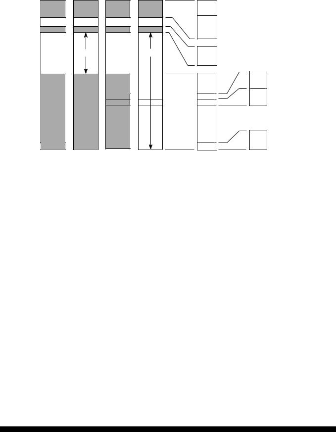
Figure 3 MC68HC11KA4/MC68HC711KA4 Block Diagram
MC68HC11KA4 |
MOTOROLA |
MC68HC11KA4TS/D |
9 |

|
TABLE OF CONTENTS |
|
Section |
|
Page |
1 |
Introduction |
1 |
1.1 |
Features ...................................................................................................................................... |
1 |
2 |
Operating Modes and On-Chip Memory |
11 |
2.1 |
Operating Modes ....................................................................................................................... |
11 |
2.2 |
On-Chip Memory ....................................................................................................................... |
11 |
3 |
Erasable Programmable Read-Only Memory |
21 |
4 |
Electrically Erasable Programmable Read-Only Memory |
23 |
5 |
Resets and Interrupts |
26 |
6 |
Parallel Input/Output |
31 |
7 |
Serial Communications Interface |
37 |
8 |
Serial Peripheral Interface |
44 |
9 |
Analog-to-Digital Converter |
48 |
10 |
Main Timer |
52 |
10.1 |
Real-Time Interrupt ................................................................................................................... |
58 |
11 |
Pulse Accumulator |
59 |
12 |
Pulse-Width Modulation Timer |
62 |
MOTOROLA |
MC68HC11KA4 |
10 |
MC68HC11KA4TS/D |
2 Operating Modes and On-Chip Memory
2.1 Operating Modes
In single-chip operating mode, the MC68HC11KA4 is a stand-alone microcontroller with no external address or data bus.
In expanded non-multiplexed operating mode, the MCU can access a 64 Kbyte physical address space. This space includes the same on-chip memory addresses used for single-chip mode, in addition to addressing capabilities for external peripheral and memory devices. The expansion bus is made up of ports B, C, and F, and the R/W signal. In expanded operating mode, high order address bits are output on the port B pins, low order address bits on the port F pins, and the data bus on port C. The R/W pin controls the direction of data transfer on the port C bus.
Bootstrap mode allows special-purpose programs to be entered into internal RAM. The bootloader program uses the serial communications interface (SCI) to read a program of up to 768 bytes into on-chip RAM. After a four-character delay, or after receiving the character for address $037F ($047F for MC68HC11KA2), control passes to the loaded program at $0080.
Special test mode is used primarily for factory testing.
2.2 On-Chip Memory
The M68HC11 CPU is capable of addressing a 64 Kbyte range. The INIT, INIT2, and CONFIG registers control the existence and locations of the registers, RAM, EEPROM, and ROM in the physical 64 Kbyte memory space. Addressing beyond the 64 Kbyte range is possible using a memory paging scheme in expanded mode only.
The 128-byte register block originates at $0000 after reset and can be placed at any other 4 Kbyte boundary ($x000) after reset by writing an appropriate value to the INIT register.
The 768-byte RAM (1024 bytes in the MC68HC11KA2) can be remapped to any 4 Kbyte boundary in memory.
The RAM in the MC68HC11KA4 is divided into two sections of 128 bytes and 640 bytes. For the MC68HC11KA4, 128 bytes of the RAM are mapped at $0000–$007F unless the registers are mapped to this space. If the registers are located in this space, the same 128 bytes of RAM are located at $0300 to $037F.
The RAM in the MC68HC11KA2 is divided into two sections of 128 bytes and 896 bytes. For the MC68HC11KA2, 128 bytes of the RAM are mapped at $0000–$007F unless the registers are mapped to this space. If the registers are located in this space, the same 128 bytes of RAM are located at $0300 to $047F.
Remapping is accomplished by writing appropriate values into the two nibbles of the INIT register. Refer to the register and RAM mapping examples following the MC68HC11KA4 and MC68HC11KA2 memory maps.
The 640-byte EEPROM is initially located at $0D80 after reset, assuming EEPROM is enabled in the memory map by the CONFIG register. EEPROM can be placed at any other 4 Kbyte boundary ($xD80) by writing appropriate values to the INIT2 register.
The ROMAD and ROMON control bits in the CONFIG register control the position and presence of ROM/EPROM in the memory map. In special test mode, the ROMON bit is forced to zero so that the ROM/EPROM is removed from the memory map. In single-chip mode, the ROMAD bit is forced to one, causing the ROM/EPROM to be enabled at $A000–$FFFF ($8000–$FFFF in the MC68HC11KA2). This guarantees that there will be ROM/EPROM at the vector space.
MC68HC11KA4 |
MOTOROLA |
MC68HC11KA4TS/D |
11 |

$0000 |
|
|
|
0000 |
128-BYTE REGISTER BLOCK |
|
|
|
|
(CAN BE REMAPPED TO ANY |
|||
|
|
|
|
007F |
||
|
|
|
|
4K PAGE BY THE INIT REGISTER) |
||
|
EXT |
|
EXT |
0080 |
768 BYTES RAM (NOTE 2) |
|
|
|
|
||||
|
|
|
|
|
(CAN BE REMAPPED TO ANY |
|
$1000 |
|
|
|
037F |
4K PAGE BY THE INIT REGISTER) |
|
|
|
|
|
|
||
|
EXT |
|
EXT |
0D80 |
640 BYTES EEPROM |
|
|
|
|
(CAN BE REMAPPED TO ANY |
|||
|
|
|
|
|
||
|
|
|
|
0FFF |
4K PAGE BY THE INIT2 REGISTER) |
|
|
|
|
|
|
|
|
$A000 |
|
|
|
A000 |
BE00 |
BOOT ROM |
|
|
|
(ONLY PRESENT IN |
|||
|
|
|
|
|
|
BOOTSTRAP MODE) |
|
|
|
|
|
BFC0 |
SPECIAL MODE |
|
|
|
|
|
BFFF |
INTERRUPT |
|
|
|
|
|
VECTORS |
|
|
|
|
|
|
|
|
|
|
|
|
|
24 KBYTES ROM/EPROM (NOTE 3) |
|
|
|
|
|
|
(CAN BE REMAPPED TO $2000–$7FFF OR |
|
|
|
|
|
|
$A000–$FFFF BY THE CONFIG REGISTER) |
|
|
|
|
|
|
FFC0 |
NORMAL MODE |
|
|
|
|
|
FFFF |
INTERRUPT |
$FFFF |
|
|
|
FFFF |
VECTORS |
|
SINGLE |
EXPANDED |
BOOTSTRAP |
SPECIAL |
|
|
|
CHIP |
|
|
TEST |
|
|
|
NOTES:
1.EPROM can be enabled in special test mode by setting the ROMON bit in the config register after reset.
2.768 bytes RAM in MC68HC711KA4, 1024 bytes RAM in MC68HC711KA2.
3.24 Kbytes ROM/EPROM in MC68HC711KA4, 32 Kbytes ROM/EPROM in MC68HC711KA2.
Figure 4 Memory Map for MC68HC11KA4
MOTOROLA |
MC68HC11KA4 |
12 |
MC68HC11KA4TS/D |
$0000 |
|
|
|
0000 |
128-BYTE REGISTER BLOCK |
|
|
|
|
(CAN BE REMAPPED TO ANY |
|||
|
|
|
|
007F |
||
|
|
|
|
4K PAGE BY THE INIT REGISTER) |
||
|
EXT |
|
EXT |
0080 |
1024 BYTES RAM (NOTE 2) |
|
|
|
|
||||
|
|
|
|
|
(CAN BE REMAPPED TO ANY |
|
$1000 |
|
|
|
047F |
4K PAGE BY THE INIT REGISTER) |
|
|
|
|
|
|
||
|
EXT |
|
EXT |
0D80 |
640 BYTES EEPROM |
|
|
|
|
(CAN BE REMAPPED TO ANY |
|||
|
|
|
|
|
||
|
|
|
|
0FFF |
4K PAGE BY THE INIT2 REGISTER) |
|
|
|
|
|
|
|
|
$8000 |
|
|
|
8000 |
BE00 |
BOOT ROM |
|
|
|
(ONLY PRESENT IN |
|||
|
|
|
|
|
|
BOOTSTRAP MODE) |
|
|
|
|
|
BFC0 |
SPECIAL MODE |
|
|
|
|
|
BFFF |
INTERRUPT |
|
|
|
|
|
VECTORS |
|
|
|
|
|
|
|
|
|
|
|
|
|
32 KBYTES ROM/EPROM (NOTE 3) |
|
|
|
|
|
|
(CAN BE REMAPPED TO $0000–$7FFF OR |
|
|
|
|
|
|
$8000–$FFFF BY THE CONFIG REGISTER) |
|
|
|
|
|
|
FFC0 |
NORMAL MODE |
|
|
|
|
|
FFFF |
INTERRUPT |
$FFFF |
|
|
|
FFFF |
VECTORS |
|
SINGLE |
EXPANDED |
BOOTSTRAP |
SPECIAL |
|
|
|
CHIP |
|
|
TEST |
|
|
|
NOTES:
1.EPROM can be enabled in special test mode by setting the ROMON bit in the config register after reset.
2.768 bytes RAM in MC68HC711KA4, 1024 bytes RAM in MC68HC711KA2.
3.24 Kbytes ROM/EPROM in MC68HC711KA4, 32 Kbytes ROM/EPROM in MC68HC711KA2.
Figure 5 Memory Map for MC68HC11KA2
MC68HC11KA4 |
MOTOROLA |
MC68HC11KA4TS/D |
13 |
|
INIT = $00 |
|
|
INIT = $10 |
|
|
INIT = $04 |
|
|
|
|
|
|
|
|
|
|
|
REG @ $0000 |
|
|
REG @ $0000 |
|
|
REG @ $4000 |
|
|
RAM @ $0080 |
|
|
RAM @ $1000 |
|
|
RAM @ $0000 |
|
|
|
|
|
|
|
|
|
|
|
$0000 |
|
|
$0000 |
|
|
$0000 |
|
|
REGISTER |
|
|
REGISTER |
|
|
RAM |
|
|
BLOCK |
|
|
BLOCK |
|
|
A |
|
|
(128 BYTES) |
|
|
(128 BYTES) |
|
|
(128 BYTES) |
|
|
$007F |
|
|
$007F |
|
|
$007F |
|
|
|
|
|
|
|
|
|
|
|
$0080 |
|
|
|
|
|
$0080 |
|
|
|
|
|
|
|
|
||
|
|
|
|
|
|
|
|
|
|
|
|
|
$1000 |
|
|
RAM |
|
|
|
|
|
RAM |
|
|
|
|
|
RAM |
|
|
|
|
B |
|
|
|
|
|
A |
|
|
(640 BYTES) |
|
|
|
B |
|
|
|
|
|
||
|
|
|
(128 BYTES) |
|
|
|
|
|
|
(640 BYTES) |
|
|
|
|
|
|
|
|
|
|
|
|
|
|
|
|
|
|
|
|
$107F |
|
|
$02FF |
|
|
$02FF |
|
|
$1080 |
|
|
|
|
|
|
|
|
|
|
|
||
|
|
|
|
|
|
|
|
|
|
|
|
|
|
|
|
|
|
|
$0300 |
|
|
RAM |
|
|
$4000 |
|
|
RAM |
|
|
|
|
REGISTER |
|
|
|
|
|
B |
|
|
|
||
|
A |
|
|
(640 BYTES) |
|
|
BLOCK |
|
|
(128 BYTES) |
|
|
|
|
|
(128 BYTES) |
|
|
$037F |
|
|
$12FF |
|
|
$407F |
|
|
|
|
|
|
|
|
|
|
|
|
|
|
|
|
|
|
|
|
|
|
|
|
|
|
|
|
Figure 6 RAM and Register Mapping for MC68HC11KA4
|
INIT = $00 |
|
|
INIT = $10 |
|
|
INIT = $04 |
|
|
|
|
|
|
|
|
|
|
|
REG @ $0000 |
|
|
REG @ $0000 |
|
|
REG @ $4000 |
|
|
RAM @ $0080 |
|
|
RAM @ $1000 |
|
|
RAM @ $0000 |
|
|
|
|
|
|
|
|
|
|
|
$0000 |
|
|
$0000 |
|
|
$0000 |
|
|
REGISTER |
|
|
REGISTER |
|
|
RAM |
|
|
BLOCK |
|
|
BLOCK |
|
|
A |
|
|
(128 BYTES) |
|
|
(128 BYTES) |
|
|
(128 BYTES) |
|
|
$007F |
|
|
$007F |
|
|
$007F |
|
|
|
|
|
|
|
|
|
|
|
$0080 |
|
|
|
|
|
$0080 |
|
|
|
|
|
|
|
|
||
|
|
|
|
|
|
|
|
|
|
|
|
|
$1000 |
|
|
RAM |
|
|
|
|
|
RAM |
|
|
|
|
|
RAM |
|
|
|
|
B |
|
|
|
|
|
A |
|
|
(896 BYTES) |
|
|
|
B |
|
|
|
|
|
||
|
|
|
(128 BYTES) |
|
|
|
|
|
|
(896 BYTES) |
|
|
|
|
|
|
|
|
|
|
|
|
|
|
|
|
|
|
|
|
$107F |
|
|
$03FF |
|
|
$03FF |
|
|
$1080 |
|
|
|
|
|
|
|
|
|
|
|
||
|
|
|
|
|
|
|
|
|
|
|
|
|
|
|
|
|
|
|
$0400 |
|
|
RAM |
|
|
$4000 |
|
|
RAM |
|
|
|
|
REGISTER |
|
|
|
|
|
B |
|
|
|
||
|
A |
|
|
(896 BYTES) |
|
|
BLOCK |
|
|
(128 BYTES) |
|
|
|
|
|
(128 BYTES) |
|
|
$047F |
|
|
$13FF |
|
|
$407F |
|
|
|
|
|
|
|
|
|
|
|
|
|
|
|
|
|
|
|
|
|
|
|
|
|
|
|
|
|
Figure 7 RAM and Register Mapping for MC68HC11KA2 |
|
|
|
|
MOTOROLA |
MC68HC11KA4 |
14 |
MC68HC11KA4TS/D |

Table 4 MC68HC11KA4 Register and Control Bit Assignments
|
Bit 7 |
6 |
5 |
4 |
3 |
2 |
1 |
Bit 0 |
|
$0000 |
PA7 |
PA6 |
PA5 |
PA4 |
PA3 |
PA2 |
PA1 |
PA0 |
PORTA |
|
|
|
|
|
|
|
|
|
|
$0001 |
DDA7 |
DDA6 |
DDA5 |
DDA4 |
DDA3 |
DDA2 |
DDA1 |
DDA0 |
DDRA |
|
|
|
|
|
|
|
|
|
|
$0002 |
DDB7 |
DDB6 |
DDB5 |
DDB4 |
DDB3 |
DDB2 |
DDB1 |
DDB0 |
DDRB |
|
|
|
|
|
|
|
|
|
|
$0003 |
DDF7 |
DDF6 |
DDF5 |
DDF4 |
DDF3 |
DDF2 |
DDF1 |
DDF0 |
DDRF |
|
|
|
|
|
|
|
|
|
|
$0004 |
PB7 |
PB6 |
PB5 |
PB4 |
PB3 |
PB2 |
PB1 |
PB0 |
PORTB |
|
|
|
|
|
|
|
|
|
|
$0005 |
PF7 |
PF6 |
PF5 |
PF4 |
PF3 |
PF2 |
PF1 |
PF0 |
PORTF |
|
|
|
|
|
|
|
|
|
|
$0006 |
PC7 |
PC6 |
PC5 |
PC4 |
PC3 |
PC2 |
PC1 |
PC0 |
PORTC |
|
|
|
|
|
|
|
|
|
|
$0007 |
DDC7 |
DDC6 |
DDC5 |
DDC4 |
DDC3 |
DDC2 |
DDC1 |
DDC0 |
DDRC |
|
|
|
|
|
|
|
|
|
|
$0008 |
0 |
0 |
PD5 |
PD4 |
PD3 |
PD2 |
PD1 |
PD0 |
PORTD |
|
|
|
|
|
|
|
|
|
|
$0009 |
0 |
0 |
DDD5 |
DDD4 |
DDD3 |
DDD2 |
DDD1 |
DDD0 |
DDRD |
|
|
|
|
|
|
|
|
|
|
$000A |
PE7 |
PE6 |
PE5 |
PE4 |
PE3 |
PE2 |
PE1 |
PE0 |
PORTE |
|
|
|
|
|
|
|
|
|
|
$000B |
FOC1 |
FOC2 |
FOC3 |
FOC4 |
FOC5 |
0 |
0 |
0 |
CFORC |
|
|
|
|
|
|
|
|
|
|
$000C |
OC1M7 |
OC1M6 |
OC1M5 |
OC1M4 |
OC1M3 |
0 |
0 |
0 |
OC1M |
|
|
|
|
|
|
|
|
|
|
$000D |
OC1D7 |
OC1D6 |
OC1D5 |
OC1D4 |
OC1D3 |
0 |
0 |
0 |
OC1D |
|
|
|
|
|
|
|
|
|
|
$000E |
Bit 15 |
14 |
13 |
12 |
11 |
10 |
9 |
Bit 8 |
TCNT (High) |
|
|
|
|
|
|
|
|
|
|
$000F |
Bit 7 |
6 |
5 |
4 |
3 |
2 |
1 |
Bit 0 |
TCNT (Low) |
|
|
|
|
|
|
|
|
|
|
$0010 |
Bit 15 |
14 |
13 |
12 |
11 |
10 |
9 |
Bit 8 |
TIC1 (High) |
|
|
|
|
|
|
|
|
|
|
$0011 |
Bit 7 |
6 |
5 |
4 |
3 |
2 |
1 |
Bit 0 |
TIC1 (Low) |
|
|
|
|
|
|
|
|
|
|
$0012 |
Bit 15 |
14 |
13 |
12 |
11 |
10 |
9 |
Bit 8 |
TIC2 (High) |
|
|
|
|
|
|
|
|
|
|
$0013 |
Bit 7 |
6 |
5 |
4 |
3 |
2 |
1 |
Bit 0 |
TIC2 (Low) |
|
|
|
|
|
|
|
|
|
|
$0014 |
Bit 15 |
14 |
13 |
12 |
11 |
10 |
9 |
Bit 8 |
TIC3 (High) |
|
|
|
|
|
|
|
|
|
|
$0015 |
Bit 7 |
6 |
5 |
4 |
3 |
2 |
1 |
Bit 0 |
TIC3 (Low) |
|
|
|
|
|
|
|
|
|
|
$0016 |
Bit 15 |
14 |
13 |
12 |
11 |
10 |
9 |
Bit 8 |
TOC1(High) |
|
|
|
|
|
|
|
|
|
|
$0017 |
Bit 7 |
6 |
5 |
4 |
3 |
2 |
1 |
Bit 0 |
TOC1 (Low) |
|
|
|
|
|
|
|
|
|
|
$0018 |
Bit 15 |
14 |
13 |
12 |
11 |
10 |
9 |
Bit 8 |
TOC2 (High) |
|
|
|
|
|
|
|
|
|
|
$0019 |
Bit 7 |
6 |
5 |
4 |
3 |
2 |
1 |
Bit 0 |
TOC2 (Low) |
|
|
|
|
|
|
|
|
|
|
$001A |
Bit 15 |
14 |
13 |
12 |
11 |
10 |
9 |
Bit 8 |
TOC3 (High) |
|
|
|
|
|
|
|
|
|
|
$001B |
Bit 7 |
6 |
5 |
4 |
3 |
2 |
1 |
Bit 0 |
TOC3 (Low) |
|
|
|
|
|
|
|
|
|
|
$001C |
Bit 15 |
14 |
13 |
12 |
11 |
10 |
9 |
Bit 8 |
TOC4 (High) |
|
|
|
|
|
|
|
|
|
|
$001D |
Bit 7 |
6 |
5 |
4 |
3 |
2 |
1 |
Bit 0 |
TOC4 (Low) |
|
|
|
|
|
|
|
|
|
|
$001E |
Bit 15 |
14 |
13 |
12 |
11 |
10 |
9 |
Bit 8 |
TI4/O5 (High) |
|
|
|
|
|
|
|
|
|
|
$001F |
Bit 7 |
6 |
5 |
4 |
3 |
2 |
1 |
Bit 0 |
TI4/O5 (Low) |
|
|
|
|
|
|
|
|
|
|
$0020 |
OM2 |
OL2 |
OM3 |
OL3 |
OM4 |
OL4 |
OM5 |
OL5 |
TCTL1 |
|
|
|
|
|
|
|
|
|
|
$0021 |
EDG4B |
EDG4A |
EDG1B |
EDG1A |
EDG2B |
EDG2A |
EDG3B |
EDG3A |
TCTL2 |
|
|
|
|
|
|
|
|
|
|
$0022 |
OC1I |
OC2I |
OC3I |
OC4I |
I4/O5I |
IC1I |
IC2I |
IC3I |
TMSK1 |
|
|
|
|
|
|
|
|
|
|
$0023 |
OC1F |
OC2F |
OC3F |
OC4F |
I4/O5F |
IC1F |
IC2F |
IC3F |
TFLG1 |
|
|
|
|
|
|
|
|
|
|
$0024 |
TOI |
RTII |
PAOVI |
PAII |
0 |
0 |
PR1 |
PR0 |
TMSK2 |
|
|
|
|
|
|
|
|
|
|
$0025 |
TOF |
RTIF |
PAOVF |
PAIF |
0 |
0 |
0 |
0 |
TFLG2 |
|
|
|
|
|
|
|
|
|
|
$0026 |
0 |
PAEN |
PAMOD |
PEDGE |
0 |
I4/O5 |
RTR1 |
RTR0 |
PACTL |
|
|
|
|
|
|
|
|
|
|
$0027 |
Bit 7 |
6 |
5 |
4 |
3 |
2 |
1 |
Bit 0 |
PACNT |
|
|
|
|
|
|
|
|
|
|
$0028 |
SPIE |
SPE |
DWOM |
MSTR |
CPOL |
CPHA |
SPR1 |
SPR0 |
SPCR |
|
|
|
|
|
|
|
|
|
|
$0029 |
SPIF |
WCOL |
0 |
MODF |
0 |
0 |
0 |
0 |
SPSR |
|
|
|
|
|
|
|
|
|
|
$002A |
Bit 7 |
6 |
5 |
4 |
3 |
2 |
1 |
Bit 0 |
SPDR |
|
|
|
|
|
|
|
|
|
|
$002B |
MBE |
0 |
ELAT |
EXCOL |
EXROW |
0 |
0 |
EPGM |
EPROG |
|
|
|
|
|
|
|
|
|
|
MC68HC11KA4 |
MOTOROLA |
MC68HC11KA4TS/D |
15 |

Table 4 MC68HC11KA4 Register and Control Bit Assignments (Continued)
|
Bit 7 |
6 |
5 |
4 |
3 |
2 |
|
1 |
Bit 0 |
|
$002C |
0 |
0 |
0 |
0 |
HPPUE |
GPPUE |
|
FPPUE |
BPPUE |
PPAR |
|
|
|
|
|
|
|
|
|
|
|
$002D |
— |
— |
— |
— |
— |
— |
— |
— |
|
Reserved |
|
|
|
|
|
|
|
|
|
|
|
$002E |
— |
— |
— |
— |
— |
— |
— |
— |
|
Reserved |
|
|
|
|
|
|
|
|
|
|
|
$002F |
— |
— |
— |
— |
— |
— |
— |
— |
|
Reserved |
|
|
|
|
|
|
|
|
|
|
|
$0030 |
CCF |
0 |
SCAN |
MULT |
CD |
CC |
|
CB |
CA |
ADCTL |
|
|
|
|
|
|
|
|
|
|
|
$0031 |
Bit 7 |
6 |
5 |
4 |
3 |
2 |
|
1 |
Bit 0 |
ADR1 |
|
|
|
|
|
|
|
|
|
|
|
$0032 |
Bit 7 |
6 |
5 |
4 |
3 |
2 |
|
1 |
Bit 0 |
ADR2 |
|
|
|
|
|
|
|
|
|
|
|
$0033 |
Bit 7 |
6 |
5 |
4 |
3 |
2 |
|
1 |
Bit 0 |
ADR3 |
|
|
|
|
|
|
|
|
|
|
|
$0034 |
Bit 7 |
6 |
5 |
4 |
3 |
2 |
|
1 |
Bit 0 |
ADR4 |
|
|
|
|
|
|
|
|
|
|
|
$0035 |
BULKP |
LVPEN |
BPRT4 |
PTCON |
BPRT3 |
BPRT2 |
|
BPRT1 |
BPRT0 |
BPROT |
|
|
|
|
|
|
|
|
|
|
|
$0036 |
— |
— |
— |
— |
— |
— |
— |
— |
|
Reserved |
|
|
|
|
|
|
|
|
|
|
|
$0037 |
EE3 |
EE2 |
EE1 |
EE0 |
0 |
0 |
|
0 |
0 |
INIT2 |
|
|
|
|
|
|
|
|
|
|
|
$0038 |
LIRDV |
CWOM |
0 |
IRVNE |
LSBF |
SPR2 |
|
XDV1 |
XDV0 |
OPT2 |
|
|
|
|
|
|
|
|
|
|
|
$0039 |
ADPU |
CSEL |
IRQE |
DLY |
CME |
FCME |
|
CR1 |
CR0 |
OPTION |
|
|
|
|
|
|
|
|
|
|
|
$003A |
Bit 7 |
6 |
5 |
4 |
3 |
2 |
|
1 |
Bit 0 |
COPRST |
|
|
|
|
|
|
|
|
|
|
|
$003B |
ODD |
EVEN |
LVPI |
BYTE |
ROW |
ERASE |
|
EELAT |
EEPGM |
PPROG |
|
|
|
|
|
|
|
|
|
|
|
$003C |
RBOOT |
SMOD |
MDA |
PSEL4 |
PSEL3 |
PSEL2 |
|
PSEL1 |
PSEL0 |
HPRIO |
|
|
|
|
|
|
|
|
|
|
|
$003D |
RAM3 |
RAM2 |
RAM1 |
RAM0 |
REG3 |
REG2 |
|
REG1 |
REG0 |
INIT |
|
|
|
|
|
|
|
|
|
|
|
$003E |
TILOP |
0 |
OCCR |
CBYP |
DISR |
FCM |
|
FCOP |
0 |
TEST1 |
|
|
|
|
|
|
|
|
|
|
|
$003F |
ROMAD |
1 |
CLKX |
PAREN |
NOSEC |
NOCOP |
|
ROMON |
EEON |
CONFIG |
|
|
|
|
|
|
|
|
|
|
|
$0040 |
— |
— |
— |
— |
— |
— |
— |
— |
|
Reserved |
to |
|
|
|
|
|
|
|
|
|
|
|
|
|
|
|
|
|
|
|
|
|
|
|
|
|
|
|
|
|
|
|
|
$005F |
— |
— |
— |
— |
— |
— |
— |
— |
|
Reserved |
|
|
|
|
|
|
|
|
|
|
|
$0060 |
CON34 |
CON12 |
PCKA2 |
PCKA1 |
0 |
PCKB3 |
|
PCKB2 |
PCKB1 |
PWCLK |
|
|
|
|
|
|
|
|
|
|
|
$0061 |
PCLK4 |
PCLK3 |
PCLK2 |
PCLK1 |
PPOL4 |
PPOL3 |
|
PPOL2 |
PPOL1 |
PWPOL |
|
|
|
|
|
|
|
|
|
|
|
$0062 |
Bit 7 |
6 |
5 |
4 |
3 |
2 |
|
1 |
Bit 0 |
PWSCAL |
|
|
|
|
|
|
|
|
|
|
|
$0063 |
TPWSL |
DISCP |
0 |
0 |
PWEN4 |
PWEN3 |
|
PWEN2 |
PWEN1 |
PWEN |
|
|
|
|
|
|
|
|
|
|
|
$0064 |
Bit 7 |
6 |
5 |
4 |
3 |
2 |
|
1 |
Bit 0 |
PWCNT1 |
|
|
|
|
|
|
|
|
|
|
|
$0065 |
Bit 7 |
6 |
5 |
4 |
3 |
2 |
|
1 |
Bit 0 |
PWCNT2 |
|
|
|
|
|
|
|
|
|
|
|
$0066 |
Bit 7 |
6 |
5 |
4 |
3 |
2 |
|
1 |
Bit 0 |
PWCNT3 |
|
|
|
|
|
|
|
|
|
|
|
$0067 |
Bit 7 |
6 |
5 |
4 |
3 |
2 |
|
1 |
Bit 0 |
PWCNT4 |
|
|
|
|
|
|
|
|
|
|
|
$0068 |
Bit 7 |
6 |
5 |
4 |
3 |
2 |
|
1 |
Bit 0 |
PWPER1 |
|
|
|
|
|
|
|
|
|
|
|
$0069 |
Bit 7 |
6 |
5 |
4 |
3 |
2 |
|
1 |
Bit 0 |
PWPER2 |
|
|
|
|
|
|
|
|
|
|
|
$006A |
Bit 7 |
6 |
5 |
4 |
3 |
2 |
|
1 |
Bit 0 |
PWPER3 |
|
|
|
|
|
|
|
|
|
|
|
$006B |
Bit 7 |
6 |
5 |
4 |
3 |
2 |
|
1 |
Bit 0 |
PWPER4 |
|
|
|
|
|
|
|
|
|
|
|
$006C |
Bit 7 |
6 |
5 |
4 |
3 |
2 |
|
1 |
Bit 0 |
PWDTY1 |
|
|
|
|
|
|
|
|
|
|
|
$006D |
Bit 7 |
6 |
5 |
4 |
3 |
2 |
|
1 |
Bit 0 |
PWDTY2 |
|
|
|
|
|
|
|
|
|
|
|
$006E |
Bit 7 |
6 |
5 |
4 |
3 |
2 |
|
1 |
Bit 0 |
PWDTY3 |
|
|
|
|
|
|
|
|
|
|
|
$006F |
Bit 7 |
6 |
5 |
4 |
3 |
2 |
|
1 |
Bit 0 |
PWDTY4 |
|
|
|
|
|
|
|
|
|
|
|
$0070 |
BTST |
BSPL |
0 |
SBR12 |
SBR11 |
SBR10 |
|
SBR9 |
SBR8 |
SCBDH |
|
|
|
|
|
|
|
|
|
|
|
$0071 |
SBR7 |
SBR6 |
SBR5 |
SBR4 |
SBR3 |
SBR2 |
|
SBR1 |
SBR0 |
SCBDL |
|
|
|
|
|
|
|
|
|
|
|
$0072 |
LOOPS |
WOMS |
0 |
M |
WAKE |
ILT |
|
PE |
PT |
SCCR1 |
|
|
|
|
|
|
|
|
|
|
|
$0073 |
TIE |
TCIE |
RIE |
ILIE |
TE |
RE |
|
RWU |
SBK |
SCCR2 |
|
|
|
|
|
|
|
|
|
|
|
$0074 |
TDRE |
TC |
RDRF |
IDLE |
OR |
NF |
|
FE |
PF |
SCSR1 |
|
|
|
|
|
|
|
|
|
|
|
$0075 |
0 |
0 |
0 |
0 |
0 |
0 |
|
0 |
RAF |
SCSR2 |
|
|
|
|
|
|
|
|
|
|
|
MOTOROLA |
MC68HC11KA4 |
16 |
MC68HC11KA4TS/D |

Table 4 MC68HC11KA4 Register and Control Bit Assignments (Continued)
|
Bit 7 |
6 |
5 |
4 |
|
3 |
|
2 |
1 |
Bit 0 |
|
$0076 |
R8 |
T8 |
0 |
0 |
|
0 |
|
0 |
0 |
0 |
SCDRH |
|
|
|
|
|
|
|
|
|
|
|
|
$0077 |
R7/T7 |
R6/T6 |
R5/T5 |
R4/T4 |
|
R3/T3 |
|
R2/T2 |
R1/T1 |
R0/T0 |
SCDRL |
|
|
|
|
|
|
|
|
|
|
|
|
$0078 |
— |
— |
— |
— |
— |
|
— |
— |
— |
|
Reserved |
to |
|
|
|
|
|
|
|
|
|
|
|
|
|
|
|
|
|
|
|
|
|
|
|
|
|
|
|
|
|
|
|
|
|
|
|
$007B |
— |
— |
— |
— |
— |
|
— |
— |
— |
|
Reserved |
|
|
|
|
|
|
|
|
|
|
|
|
$007C |
0 |
0 |
0 |
0 |
|
PH3 |
|
PH2 |
PH1 |
PH0 |
PORTH |
|
|
|
|
|
|
|
|
|
|
|
|
$007D |
0 |
0 |
0 |
0 |
|
DDH3 |
|
DDH2 |
DDH1 |
DDH0 |
DDRH |
|
|
|
|
|
|
|
|
|
|
|
|
$007E |
PG7 |
0 |
0 |
0 |
|
0 |
|
0 |
0 |
0 |
PORTG |
|
|
|
|
|
|
|
|
|
|
|
|
$007F |
DDG7 |
0 |
0 |
0 |
|
0 |
|
0 |
0 |
0 |
DDRG |
|
|
|
|
|
|
|
|
|
|
|
|
HPRIO — Highest Priority I-Bit Interrupt and Miscellaneous |
|
|
$003C |
||||||
|
Bit 7 |
6 |
5 |
4 |
3 |
2 |
1 |
Bit 0 |
|
|
|
|
|
|
|
|
|
|
|
|
RBOOT* |
SMOD* |
MDA* |
PSEL4 |
PSEL3 |
PSEL2 |
PSEL1 |
PSEL0 |
|
|
|
|
|
|
|
|
|
|
|
RESET: |
0 |
0 |
0 |
0 |
0 |
1 |
1 |
0 |
Single Chip |
|
0 |
0 |
1 |
0 |
0 |
1 |
1 |
0 |
Expanded |
|
1 |
1 |
0 |
0 |
0 |
1 |
1 |
0 |
Bootstrap |
|
0 |
1 |
1 |
0 |
0 |
1 |
1 |
0 |
Special Test |
*The reset values of RBOOT, SMOD, and MDA depend on the mode selected at power up.
RBOOT — Read Bootstrap ROM
Valid only when SMOD is set to one (bootstrap or special test mode). Can only be written in special mode.
0 = Bootloader ROM disabled and not in map
1 = Bootloader ROM enabled and in map at $BE00–$BFFF
SMOD and MDA —Special Mode Select and Mode Select A
These two bits can be read at any time. SMOD can only be written to zero. MDA can only be written once in normal modes or any time in special modes.
Inputs |
|
|
Latched at Reset |
||
|
|
|
|
|
|
MODB |
|
MODA |
Mode |
SMOD |
MDA |
|
|
|
|
|
|
1 |
|
0 |
Single Chip |
0 |
0 |
|
|
|
|
|
|
1 |
|
1 |
Expanded |
0 |
1 |
|
|
|
|
|
|
0 |
|
0 |
Bootstrap |
1 |
0 |
|
|
|
|
|
|
0 |
|
1 |
Special Test |
1 |
1 |
|
|
|
|
|
|
PSEL[4:0] —Priority Select Bits [4:0]
Refer to 5 Resets and Interrupts.
MC68HC11KA4 |
MOTOROLA |
MC68HC11KA4TS/D |
17 |

INIT —RAM and I/O Register Mapping |
|
|
|
|
$003D |
|||
|
Bit 7 |
6 |
5 |
4 |
3 |
2 |
1 |
Bit 0 |
|
|
|
|
|
|
|
|
|
|
RAM3 |
RAM2 |
RAM1 |
RAM0 |
REG3 |
REG2 |
REG1 |
REG0 |
|
|
|
|
|
|
|
|
|
RESET: |
0 |
0 |
0 |
0 |
0 |
0 |
0 |
0 |
Can be written only once in first 64 cycles out of reset in normal modes or at any time in special mode.
RAM[3:0] —Internal RAM Map Position
Specifies upper four bits of RAM address. At reset, RAM is mapped to $0000 along with register block.
REG[3:0] —128-Byte Register Block Map Position
Specifies upper four bits of register space address. At reset, registers are mapped to $0000.
CONFIG —COP, ROM Mapping, EEPROM Enables |
|
|
|
$003F |
|||||
|
Bit 7 |
6 |
5 |
4 |
3 |
2 |
1 |
Bit 0 |
|
|
|
|
|
|
|
|
|
|
|
|
ROMAD |
— |
CLKX |
PAREN |
NOSEC |
NOCOP |
ROMON |
EEON |
|
|
|
|
|
|
|
|
|
|
|
RESET: |
— |
1 |
— |
— |
— |
— |
— |
— |
|
CONFIG is made up of EEPROM cells and static working latches. The operation of the MCU is controlled directly by these latches and not the actual EEPROM byte. When programming the CONFIG register, the EEPROM byte is being accessed. When the CONFIG register is being read, the static latches are being accessed.
These bits can be read at any time. The value read is the one latched into the register from the EEPROM cells during the last reset sequence. A new value programmed into this register cannot be read until after a subsequent reset sequence. Unused bits always read as ones.
If SMOD = 1, CONFIG bits can be written at any time. If SMOD = 0 CONFIG bits can only be written using the EEPROM programming sequence, and are neither readable nor active until latched via the next reset.
ROMAD — ROM/EPROM Mapping Control
In single-chip mode ROMAD is forced to one out of reset.
0 = ROM/EPROM located at $2000–$7FFF ($2000–$9FFF in MC68HC11KA2) 1 = ROM/EPROM located at $A000–$FFFF ($8000–$FFFF in MC68HC11KA2)
Bit 6 — Not implemented
Always reads one
CLKX — XOUT Clock Enable 0 = XOUT pin disabled
1 = x clock driven out on the XOUT pin
PAREN — Pull-Up Assignment Register Enable
Refer to 6 Parallel Input/Output.
NOSEC — Security Disable
NOSEC is invalid unless the security mask option is specified before the MCU is manufactured. If security mask option is omitted NOSEC always reads one.
0 = Security enabled
1 = Security disabled
MOTOROLA |
MC68HC11KA4 |
18 |
MC68HC11KA4TS/D |

NOCOP — COP System Disable Resets to programmed value
0 = COP enabled (forces reset on time-out)
1 = COP disabled (does not force reset on time-out)
ROMON — ROM/EPROM Enable
In single-chip mode, ROMON is forced to one out of reset. In special test mode, ROMON is forced to zero out of reset.
0 = ROM/EPROM removed from memory map
1 = ROM/EPROM present in memory map
EEON — EEPROM Enable
0 = EEPROM disabled from memory map
1 = EEPROM present in memory map with location depending on value specified in EE[3:0] in INIT2
OPT2 —System Configuration Options 2 |
|
|
|
|
$0038 |
|||
|
Bit 7 |
6 |
5 |
4 |
3 |
2 |
1 |
Bit 0 |
|
|
|
|
|
|
|
|
|
|
— |
CWOM |
— |
IRVNE |
LSBF |
SPR2 |
XDV1 |
XDV0 |
|
|
|
|
|
|
|
|
|
RESET: |
0 |
0 |
0 |
— |
0 |
0 |
0 |
0 |
Bit 7 — Not implemented
Always reads zero
CWOM — Port C Wired-OR Mode
Refer to 6 Parallel Input/Output.
Bit 5 — Not implemented
Always reads zero
IRVNE — Internal Read Visibility/Not E
Can be written at any time if SMOD = 1. If SMOD = 0, only one write is allowed. In expanded mode, IRVNE determines whether IRV is on or off. In special test mode, IRVNE is reset to one. In all other modes, IRVNE is reset to zero.
0 = No internal read visibility on external bus
1 = Data from internal reads is driven out of the external data bus.
In single-chip modes, this bit determines whether the E clock drives out from the chip. 0 = E is driven out from the chip.
1 = E pin is driven low.
Mode |
IRVNE Out |
E Clock Out of |
IRV Out of |
IRVNE |
IRVNE |
|
of Reset |
Reset |
Reset |
Affects Only |
Can Be Written |
|
|
|
|
|
|
Single Chip |
0 |
On |
Off |
E |
Once |
|
|
|
|
|
|
Expanded |
0 |
On |
Off |
IRV |
Once |
|
|
|
|
|
|
Boot |
0 |
On |
Off |
E |
Once |
|
|
|
|
|
|
Special Test |
1 |
On |
On |
IRV |
Once |
|
|
|
|
|
|
LSBF — SPI LSB First Enable
Refer to 8 Serial Peripheral Interface.
SPR2 — SPI Clock Rate Select
Refer to 8 Serial Peripheral Interface.
MC68HC11KA4 |
MOTOROLA |
MC68HC11KA4TS/D |
19 |

XDV[1:0] — XOUT Clock Divide Select
These two bits control the frequency of the clock that is driven out the XOUT pin. The CLKX bit in the CONFIG register controls whether this clock is on or off. When a clock rate is selected, allow a maximum of 16 cycles for stabilization. During reset a frequency of EXTAL is output. This frequency can be divided after reset. Note that the phase relationship between the 4XDV1 signal and both EXTAL and E cannot be predicted. Refer to the following table for further information about XOUT frequencies.
Table 5 XOUT Frequencies
|
XDV[1:0] |
EXTAL |
Frequency at |
Frequency at |
Frequency at |
|
|
Divided By |
EXTAL = 8 MHz |
EXTAL = 12 MHz |
EXTAL = 16 MHz |
|
|
|
|
|
|
0 |
0 |
1 |
8 MHz |
12 MHz |
16 MHz |
|
|
|
|
|
|
0 |
1 |
4 |
2 MHz |
3 MHz |
4 MHz |
|
|
|
|
|
|
1 |
0 |
6 |
1.33 MHz |
2 MHz |
2.7 MHz |
|
|
|
|
|
|
1 |
1 |
8 |
1 MHz |
1.5 MHz |
2 MHz |
|
|
|
|
|
|
|
XDV[1:0] |
EXTAL |
Frequency at |
Frequency at |
Frequency at |
|
|
Divided By |
EXTAL = 8.4 MHz |
EXTAL = 12.6 MHz |
EXTAL = 16.8 MHz |
|
|
|
|
|
|
0 |
0 |
1 |
8.4 MHz |
12.6 MHz |
16.8 MHz |
|
|
|
|
|
|
0 |
1 |
4 |
2.1 MHz |
3.15 MHz |
4.2 MHz |
|
|
|
|
|
|
1 |
0 |
6 |
1.4 MHz |
2.1 MHz |
2.8 MHz |
|
|
|
|
|
|
1 |
1 |
8 |
1.05 MHz |
1.57 MHz |
2.1 MHz |
|
|
|
|
|
|
NOTE
The XOUT pin is not bonded in the 64-pin package.
MOTOROLA |
MC68HC11KA4 |
20 |
MC68HC11KA4TS/D |
3 Erasable Programmable Read-Only Memory
The MC68HC711KA4 has 24 Kbytes of ROM/EPROM. The MC68HC711KA2 has 32 Kbytes of ROM/ EPROM. In all parts, the ROM/EPROM can be mapped to one of two locations in the memory map. The locations are as follows:
In the MC68HC11KA4, the ROM/EPROM can be mapped at $2000–$7FFF or $A000–$FFFF. If it is mapped to $A000–$FFFF, vector space is included. In single-chip mode the MC68HC11KA4 ROM/ EPROM is forced to $A000–$FFFF (ROMAD = 1) and enabled (ROMON = 1), regardless of the value in the CONFIG register.
In the MC68HC11KA2, the ROM/EPROM can be mapped at $0000–$7FFF or $8000–$FFFF. If it is mapped to $8000–$FFFF, vector space is included. In single-chip mode the MC68HC11KA2 ROM/ EPROM is forced to $8000–$FFFF (ROMAD = 1) and enabled (ROMON = 1), regardless of the value in the CONFIG register.
In PROG mode, the EPROM/OTPROM is programmed as a stand-alone EPROM by adapting the MCU footprint to the 27256-type EPROM and using an appropriate EPROM programmer. Programming EPROM/OTPROM requires an external 12.25 volt nominal power supply (VPPE). There are two methods that can be used to program and verify EPROM/OTPROM.
In normal MCU mode, EPROM/OTPROM can be programmed in any operating mode —special test, bootstrap, expanded, or single chip. Normal programming is completed using the EPROG register.
To program the EPROM, complete the following steps using the EPROG register:
1.Write to EPROG with the ELAT bit set.
2.Write data to the desired address.
3.Write to EPROG with the ELAT and EPGM bits set.
4.Delay for 10 ms or more, as appropriate.
5.Clear the EPGM bit in EPROG to turn off the VPPE voltage.
6.Clear the EPROG register to reconfigure the EPROM address and data buses for normal operation.
EPROG —EPROM Programming Control |
|
|
|
|
|
|
$002B |
|||
|
Bit 7 |
6 |
5 |
4 |
3 |
|
2 |
1 |
|
Bit 0 |
|
|
|
|
|
|
|
|
|
|
|
|
MBE |
— |
ELAT |
EXCOL |
EXROW |
— |
|
— |
|
EPGM |
|
|
|
|
|
|
|
|
|
|
|
RESET: |
0 |
0 |
0 |
0 |
0 |
|
0 |
0 |
0 |
|
MBE — Multiple Byte Program Enable
Used for factory test purposes only
Bit 6 — Not implemented
Always reads zero
ELAT — EPROM Latch Control
If ELAT = 1, EPROM is in programming mode and cannot be read. If ELAT = 1, writes to EPROM cause address and data to be latched.
0 = EPROM address and data bus configured for normal reads 1 = EPROM address and data bus configured for programming
EXCOL — Select Extra Columns
Used for factory test purposes only
EXROW — Select Extra Row
Used for factory test purposes only
Bits [2:1] — Not implemented
Always read zero
MC68HC11KA4 |
MOTOROLA |
MC68HC11KA4TS/D |
21 |
 Loading...