


 Loading...
Motorola MC68SEC000PB16, MC68SEC000PB20, MC68SEC000CPB10, MC68SEC000CPB20, MC68SEC000FU10 Datasheet
...Order this document by
M68000UMAD/AD
Communications and Advanced |
M68000 |
Consumer Technologies Group |
|
|
Addendum to
M68000
User Manual
August 7, 1997
This addendum to the M68000UM/AD User’s Manual, Revision 8, provides corrections to the original text as well as additional information. This document and other information on this product is maintained on the World Wide Web at http://www.motorola.com/68000.
OVERVIEW
This manual includes hardware details and programming information for the MC68HC000, the MC68HC001, the MC68EC000, and the MC68SEC000. For ease of reading, the name M68000 MPUs will be used when referring to all processors. Refer to M68000PM/AD, M68000 Programmer's Reference Manual, for detailed information on the MC68000 instruction set.
The four microprocessors are very similar to each other and all contain the following features:
•Sixteen 32-Bit Data and Address Registers
•16-Mbyte Direct Addressing Range
•Program Counter
•6 Instruction Types
•Operations on Five Main Data Types
•Memory-Mapped Input/Output (I/O)
•14 Addressing Modes
The following processors contain additional features:
•MC68HC001/MC68EC000/MC68SEC000
—Statically selectable 8- or 16-bit data bus
•MC68HC000/MC68EC000/MC68HC001/MC68SEC000
—Low power
This document contains information on a product under development. Motorola reserves the right to change or discontinue this product without notice.
SEMICONDUCTOR PRODUCT INFORMATION
1997 Motorola, Inc. All Rights Reserved.

The primary features of the MC68SEC000 embedded processor include the following:
•Direct Replacement for the MC68EC000
—Pin-for-pin compatibility with the MC68EC000 in the plastic QFP and TQFP packages
—Vast selection of existing third-party development tools for the MC68EC000 support the MC68SEC000
—Software written for the MC68EC000 will run unchanged on the MC68SEC000
•Power Management
—Low-power HCMOS technology
—Static design allows for stopping the processor clock
—3.3V or 5V operation
—Typical 0.5 A current consumption at 3.3V in sleep mode
•Software Strength
—Fully upward object-code compatible with other M68000 Family products
—M68000 architecture allows effective assembly code with a C compiler
•Upgrade
—Fully upward code-compatible with higher performance 680x0 and 68300 Family members
—ColdFire® code-compatible with minor modifications
1.MC68HC000
The primary benefit of the MC68HC000 is reduced power consumption. The device dissipates less power (by an order of magnitude) than the NMOS MC68000.
The MC68HC000 is an implementation of the M68000 16/-32 bit microprocessor architecture. The MC68HC000 has a 16-bit data bus implementation of the MC68000 and is upward code-compatible with the MC68010 and the MC68020 32-bit implementation of the architecture.
1.1 MC68HC001
The MC68HC001 provides a functional extension to the MC68HC000 HCMOS 16-/32-bit microprocessor with the addition of statically selectable 8- or 16-bit data bus operation. The MC68HC001 is object-code compatible with the MC68HC000. You can migrate code written for the MC68HC001 without modification to any member of the M68000 Family.
1.2 MC68EC000
The MC68EC000 is an economical high-performance embedded controller designed to suit the needs of the cost-sensitive embedded-controller market. The HCMOS MC68EC000 has an internal 32-bit architecture that is supported by a statically selectable 8- or 16-bit data bus. This architecture provides a fast and efficient processing device that can satisfy the requirements of sophisticated applications based on high-level languages.
The MC68EC000 is fully object-code compatible with the MC68000. You can migrate code written for the MC68EC000 without modification to any member of the M68000 Family.
The MC68EC000 brings the performance level of the M68000 Family to cost levels previously associated with 8-bit microprocessors. The MC68EC000 benefits from the rich M68000 instruction set and its related high code density with low memory bandwidth requirements.
2 |
M68000 USER’S MANUAL ADDENDUM |
MOTOROLA |

1.3 MC68SEC000
The MC68SEC000 is a cost-effective static embedded processor engineered for low-power applications. In addition to providing the substantial cost and performance benefits of the MC68EC000, the low-power mode of the MC68SEC000 provides significant advantages in power consumption and power management. The typical current consumption of the MC68SEC000 is only 0.5 A in static standby mode and 15.0mA in normal 3.3V operation. The MC68SEC000 operates in either 3.3V or 5.0V systems. The remarkably low power consumption, small footprint packages, and static implementation are combined in the MC68SEC000 for lowpower applications such as portable measuring equipment, electronic games, and battery-operated hand-held consumer products.
The HCMOS MC68SEC000’s static architecture is a direct replacement for the MC68EC000, which offers the lowest cost entry point to 32-bit processing. The internal 32-bit architecture provides fast and efficient processing that satisfies the requirements of sophisticated applications based on high-level languages.
All of the existing third-party developer tools widely available for the MC68EC000 will directly support the MC68SEC000. You can find detailed descriptions of these tools in the High Performance Embedded Systems Source Catalog.
MOTOROLA |
M68000 USER’S MANUAL ADDENDUM |
3 |
2.0 SIGNAL DESCRIPTION
Change Figure 3-3 on Page 3-2.
|
VCC |
A23-A0 |
ADDRESS BUS |
|
|
GND |
|
|
|
|
CLK |
D15-D0 |
DATA BUS |
|
|
|
|||
|
|
AS |
|
|
|
FC0 |
R/W |
|
|
PROCESSOR |
FC1 |
ASYNCHRONOUS |
||
UDS |
||||
STATUS |
FC2 |
BUS CONTROL |
||
LDS |
||||
|
|
|
||
|
|
DTACK |
|
|
|
|
MC68SEC000 |
|
|
|
|
BR |
BUS ARBITRATION |
|
|
|
BG |
||
|
|
CONTROL |
||
|
BERR |
IPL0 |
|
|
|
IPL1 |
|
||
|
RESET |
|
||
SYSTEM |
|
INTERRUPT |
||
|
IPL2 |
|||
CONTROL |
HALT |
CONTROL |
||
AVEC |
||||
|
MODE |
|
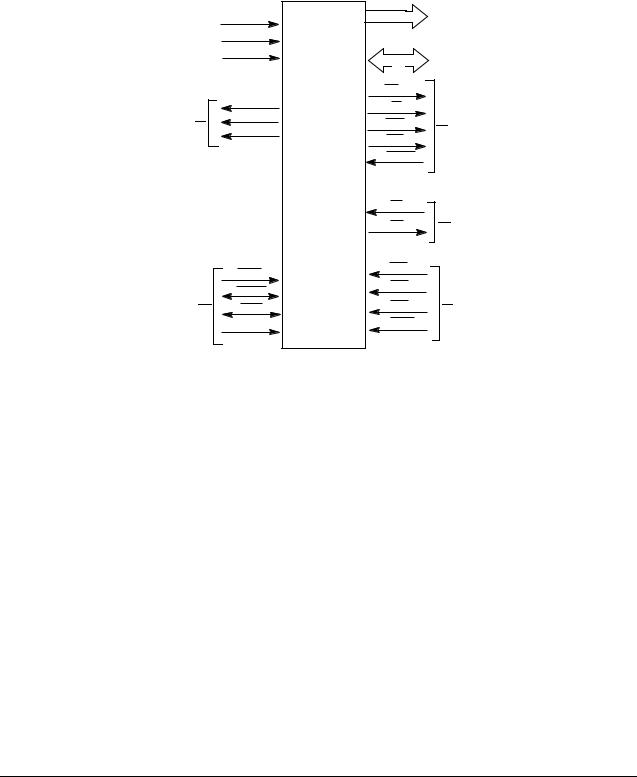
Figure 1. Input and Output Signals (MC68EC000 and MC68SEC000)
2.1 Data Bus (D15-D0)
In Section 3.2 on page 3-4, replace “The MC68EC000 and MC68HC001 use D7-D0 in 8-bit mode, and D15D8 are undefined.” with “Using the MC68HC001, MC68EC000, and MC68SEC000 mode pin, you can statically select either 8- or 16-bit modes for data transfer. The MC68EC000, MC68SEC000, and MC68HC001 use D7-D0 in 8-bit mode. D15-D8 are undefined.”
2.2 Bus Arbitration Control
In Section 3.4 on page 3-5, the sentence “In the 48-pin version of the MC68008 and MC68EC000, no pin is available for the bus grant acknowledge signal; this microprocessor uses a two-wire bus arbitration scheme.” should read “In the 64-pin MC68EC000 and MC68SEC000, no pin is available for the bus grant acknowledge signal. These microprocessors use a two-wire bus arbitration scheme.”
2.3 System Control
The Mode subsection heading of Section 3.6 on page 3-7 should read ‘‘Mode (MODE) (MC68HC001/ 68EC000/68SEC000).’’
2.4 MC68SEC000 Low-Power Mode
Add the following to Sections 4 and 5, Bus Operation.
The MC68SEC000 has been redesigned to provide fully staticand low-power operation. This section describes the recommended method for placing the MC68SEC000 into a low-power mode to reduce the
4 |
M68000 USER’S MANUAL ADDENDUM |
MOTOROLA |
power consumption to its quiescent value1 while maintaining the internal state of the processor. The low-power mode described below will be routinely tested as part of the MC68SEC000 test vectors provided by Motorola.
To successfully enter the low-power mode, the MC68SEC000 must first be in the supervisor mode. A recommended method for entering the low-power mode is to use the TRAP instruction, which causes the processor to begin exception processing, thus entering the supervisor mode. External circuitry should accomplish the following steps during the trap routine:
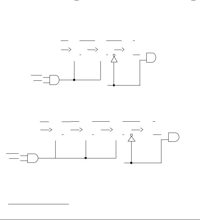
1.Externally detect a write to the low-power address. You select this address which can be any address in the 16 Mbyte addressing range of the MC68SEC000. A write to the low-power address can be detected by polling A23–A0, R/W, and FC2–FC0. When the low-power address is detected, R/W is a logic low, and the function codes have a five (101) on their output, the processor is writing to the low-power address in supervisor mode and user-designed circuitry should assert the ADDRESS_MATCH signal shown in Figure 2 and Figure 3.
ADDRESS_MATCH |
|
|
|
|
D |
Q |
|
|
|
D Q |
|
|
|
D Q |
|
|
|
|
|
|||||||||
|
|
|
||||||||||||||||||||||||||
|
|
|
|
|
|
CK |
|
|
|
|
|
CK |
|
|
|
CK |
|
|
|
|
|
|||||||
|
|
AS |
|
|
|
|
|
AS |
|
|
|
|
|
|
|
|
||||||||||||
|
|
|||||||||||||||||||||||||||
|
|
|
|
|
|
|
|
|
|
|
|
|
|
|
|
|
|
|
|
|
|
|
|
|
|
|
|
|
|
|
|
|
|
|
|
|
Q |
|
|
|
|
|
Q |
|
|
|
Q |
|
|
|
|
CPU_CLK |
|||||
|
|
|
|
|
|
|
|
|
||||||||||||||||||||
|
|
|
|
|
|
|
|
|
|
|
|
|
|
|
|
|
|
|||||||||||
|
|
|
|
|
|
CL |
|
|
|
|
|
|
CL |
|
|
|
|
|
|
|
|
|
|
|||||
|
|
|
|
|
|
|
|
|
|
|
|
|
|
|
|
|
|
|
|
|
|
|||||||
|
|
|
|
|
|
|
|
|
|
|
|
|
|
|
|
|
|
|
|
|
|
|
||||||
RESTART
RESET
SYSTEM_CLK
Figure 2. MC68SEC000 Low-Power Circuitry for 16-Bit Data Bus
ADDRESS_MATCH |
|
|
|
|
D |
Q |
|
|
|
D |
Q |
|
|
|
D Q |
|
|
|
D Q |
|
|
|
|
|
||||||||||||
|
|
|
||||||||||||||||||||||||||||||||||
|
|
|
|
|
|
CK |
|
|
|
|
|
CK |
|
|
|
|
|
|
CK |
|
|
|
CK |
|
|
|
|
|
||||||||
|
|
AS |
|
|
|
|
|
AS |
|
|
|
AS |
|
|
|
|
|
|
|
|
|
|||||||||||||||
|
|
|||||||||||||||||||||||||||||||||||
|
|
|
|
|
|
|
|
|
|
|
|
|
|
|
|
|
|
|
|
|
|
|
|
|
|
|
|
|
|
|
|
|
|
|
|
|
|
|
|
|
|
|
|
|
Q |
|
|
|
|
|
|
Q |
|
|
|
|
|
|
|
Q |
|
|
|
|
|
Q |
|
|
|
|
|
CPU_CLK |
|
|
|
|
|
|
|
|
|
|
|
|
|
|
|
|
|
|
|
|
|
|
||||||||||||||||
|
|
|
|
|
|
CL |
|
|
|
|
|
CL |
|
|
|
|
|
|
CL |
|
|
|
|
|
|
|
|
|
|
|||||||
|
|
|
|
|
|
|
|
|
|
|
|
|
|
|
|
|
|
|
|
|
|
|
|
|
|
|
||||||||||
|
|
|
|
|
|
|
|
|
|
|
|
|
|
|
|
|
|
|
|
|
|
|
|
|
|
|
|
|||||||||
RESTART
RESET
SYSTEM_CLK
Figure 3. MC68SEC000 Low-Power Circuitry for 8-Bit Data Bus
2.Execute the STOP instruction. The external circuitry shown in Figure 2 and Figure 3 will count the number of bus cycles starting with the write to the low-power address and will stop the processor clock on the first falling edge of the system clock after the bus cycle that reads the immediate data of the STOP instruction. Figure 3 has one more flip-flop than Figure 2 because the MC68SEC000 in
1.The preliminary specification for the MC68SEC000’s current drain while in the low-power mode is Idd < 2 A for 3.3V operation and Idd < 5 A for 5.0V operation.
5 |
M68000 USER’S MANUAL ADDENDUM |
MOTOROLA |

8-bit mode requires two bus cycles to fetch the immediate data of the STOP instruction. After the processor clock is disabled, it is often necessary to disable the clock to other sections of your circuit. This can be done, but be careful that runt clocks and spurious glitches are not presented to the MC68SEC000. A timing diagram is shown in Figure 4.
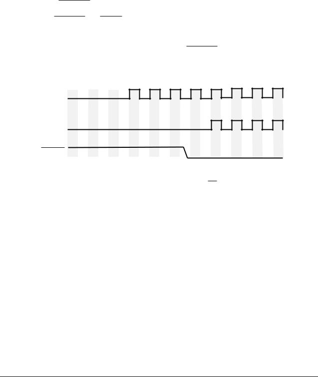
CLK
S0 S1 S2 S3 S4 S5 S6 S7 S0 S1 S2 S3 S4 S5 S6 S7
CPU_CLK
AS
RW
DTACK
Write to |
Fetch Immediate |
Stop |
Low-Power |
Data of STOP |
|
Address |
Instruction |
|
Figure 4. MC68SEC000 Clock Stop Timing for 16-Bit Data Bus
Note: While the MC68SEC000 is in the low-power mode, all inputs must be driven to VDD or VSS, or have a pull-up or pull-down resistor.
3.This step is optional depending on whether your applications require the MC68SEC000 signals with three-state capability to be placed into a high-impedance state. To place the MC68SEC000 into a three-state condition, the proper method for arbitrating the bus (as described in 5.2 Bus Arbitration in the M68000 User’s Manual, Rev 8) should be completed during the fetch of the status register data for the STOP instruction. A timing diagram with the bus arbitration sequence is shown in Figure 5.
CLK
S0 S1 S2 S3 S4 S5 S6 S7 S0 S1 S2 S3 S4 S5 S6 S7
CPU_CLK
AS
RW
DTACK
BR
BG
Write to |
Fetch Immediate |
Stop |
Low-Power |
Data of STOP |
|
Address |
Instruction |
|
Figure 5. MC68SEC000 Clock Stop Timing with Bus Arbitration for 16-Bit Data Bus
6 |
M68000 USER’S MANUAL ADDENDUM |
MOTOROLA |
After the previous steps are completed, the MC68SEC000 will remain in the low-power mode until it recognizes the appropriate interrupt . External logic will also have to poll IPLB2–IPLB0 to detect the proper interrupt. When the correct interrupt level is received, the following steps will bring the processor out of the low-power mode:
1.Restart the system clock if it was stopped.
2.Wait for the system clock to become stable.
3.Assert the RESTART signal. This will cause the processor’s clock to start on the next falling edge of the system clock. Figure 6 shows the timing for bringing the processor out of the low-power mode. Both the RESTART and RESET signals are subject to the asynchronous setup time as specified in the Electrical Characteristics section of this addendum.
WARNING
The system clock must be stable before the RESTART signal is asserted to prevent glitches in the clock. An unstable clock can cause unpredictable results in the MC68SEC000.
CLK
CPU_CLK
RESTART
Figure 6. MC68SEC000 Clock Start Timing
4.If the MC68SEC000 was placed in a three-state condition, the BR signal must be negated before the processor can begin executing instructions.
7 |
M68000 USER’S MANUAL ADDENDUM |
MOTOROLA |

An example trap routine is as follows: |
|
TRAP_x MOVE.B #0,$low_power_address |
/* Write that causes ADDRESS_MATCH to assert */ |
STOP #$2000 |
/* STOP instruction with desired interrupt mask */ |
RTE |
/* Return from the exception */ |
The first instruction (MOVE.B #0,$low_power_address) writes a byte to the low-power address that will cause the external circuitry to begin the sequence that will stop the processor’s clock. The second instruction (STOP #$2000) loads the SR with the immediate data. This lets you set the interrupt that will cause the processor to come out of the low-power mode. The final instruction (RTE) tells the processor to return from the exception and resume normal processing.
3.0 MC68SEC000 ELECTRICAL SPECIFICATIONS
Add to the following table to Section 10.1.
3.1 MC68SEC000 MAXIMUM RATINGS
RATING |
SYMBOL |
VALUE |
UNIT |
Supply Voltage |
VCC |
–0.3 to 6.5 |
V |
Input Voltage |
Vin |
–0.5 to 6.5 |
V |
Maximum Operating |
TA |
TL to TH |
°C |
Temperature Range |
|
0 to 70 |
|
Commercial Extended "C" Grade |
|
–40 to 85 |
|
|
|
|
|
Storage Temperature |
Tstg |
–55 to 150 |
°C |
|
|
|
|
3.2 CMOS CONSIDERATIONS
The following change should be made to Section 10.4, CMOS Considerations.
“Although the MC68HC000 and MC68EC000 is implemented with input protection diodes, care should be exercised to ensure that the maximum input voltage specification is not exceeded.” should read “Although the MC68HC000, MC68EC000, and MC68SEC000 are implemented with input protection diodes, be careful not to exceed the maximum input voltage specification.”
8 |
M68000 USER’S MANUAL ADDENDUM |
MOTOROLA |
Loading...