MOTOROLA MC74ACT109N, MC74ACT109ML1, MC74ACT109ML2, MC74ACT109MR2, MC74ACT109DR2 Datasheet
...
Dual JK Positive Edge Triggered Flip Flop
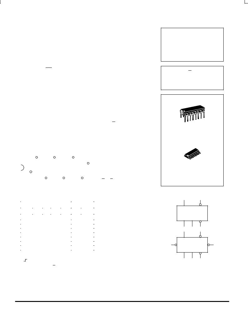
The MC74AC109/74ACT109 consists of two high-speed completely independent transition clocked JK flip-flops. The clocking operation is independent of rise and fall times of the clock waveform. The JK design allows operation as a D flip-flop (refer to MC74AC74/74ACT74 data sheet) by connecting the J and K inputs together.
Asynchronous Inputs:
LOW input to SD (Set) sets Q to HIGH level LOW input to CD (Clear) sets Q to LOW level Clear and Set are independent of clock
Simultaneous LOW on CD and SD makes both Q and Q HIGH
•Outputs Source/Sink 24 mA
•′ACT109 Has TTL Compatible Inputs
VCC |
|
CD2 |
|
|
J2 |
|
K2 |
|
CP2 |
|
SD2 |
Q2 |
|
|
|
Q2 |
|
|
|
|
|
|
|
|
|
|
|||||||||||||||
|
16 |
|
|
15 |
|
14 |
|
13 |
|
12 |
|
11 |
|
10 |
|
|
|
9 |
|
|
|
|
|
|
|
|
|
|
|
||||||||||||
|
|
|
|
|
|
|
|
|
|
|
|
|
|
|
|
|
|
|
|
|
|
|
|
|
|
|
|
|
|
|
|
|
|
|
|
|
|
|
|
||
|
|
|
|
|
|
|
|
|
|
|
|
|
|
|
|
|
|
|
|
|
|
|
|
|
|
|
|
|
|
|
|
|
|
|
|
|
|
|
|
|
|
|
|
|
|
|
|
CD |
|
|
J |
|
K |
|
CP |
|
SD |
|
Q |
Q |
|
|
|
|
|
|
|
|
|
|
|
|
|
|
|||||||||
|
|
|
|
|
|
|
|
|
|
|
|
|
|
|
|
|
|
|
|
|
|
|
|
|
|
|
|
|
|
PIN NAMES |
|
||||||||||
|
|
|
|
|
|
|
|
|
|
|
|
|
|
|
|
|
|
|
|
|
|
|
|
|
|
|
|
|
|
|
|
|
|||||||||
|
|
|
|
|
|
|
|
|
|
|
|
|
|
|
|
|
|
|
|
|
|
|
|
|
|
|
|
|
|
|
|
|
|
|
|
|
|
|
|
|
|
|
|
|
|
|
CD1 |
|
|
K1 |
|
CP1 |
|
SD1 |
|
Q1 |
|
Q1 |
|
|
|
|
|
|
J1, J2, K1, K2 |
Data Inputs |
|||||||||||||||||
|
|
|
|
|
|
J1 |
|
|
|
|
|
|
|
|
|
|
|
|
|||||||||||||||||||||||
|
|
|
|
|
|
|
|
|
|
|
|
|
|
|
|
|
|
|
|
|
|
|
|
|
|
|
|
|
|
|
|
|
CP1, |
CP2 |
Clock Pulse Inputs |
||||||
|
|
|
|
|
|
|
|
|
|
|
|
|
|
|
|
|
|
|
|
|
|
|
|
|
|
|
|
|
|
|
|
|
C |
D1, |
C |
D2 |
Direct Clear Inputs |
||||
|
1 |
|
|
2 |
|
3 |
|
4 |
|
5 |
|
6 |
|
7 |
|
|
|
8 |
|
SD1, SD2 |
|
|
Direct Set Inputs |
||||||||||||||||||
|
CD1 |
|
J1 |
|
|
K1 |
|
CP1 |
|
SD1 |
|
Q1 |
Q1 |
|
|
GND |
Q1, Q2, Q1, Q2 |
Outputs |
|||||||||||||||||||||||
TRUTH TABLE
|
|
|
Inputs |
|
|
Outputs |
||||||
|
|
|
|
|
|
|
|
|
|
|
|
|
|
SD |
CD |
CP |
J |
K |
Q |
|
Q |
||||
|
L |
H |
|
X |
X |
X |
H |
|
L |
|||
|
H |
L |
|
X |
X |
X |
L |
|
H |
|||
|
L |
L |
|
X |
X |
X |
H |
|
H |
|||
|
H |
H |
|
|
|
|
L |
L |
L |
|
H |
|
|
|
|
|
|
|
|||||||
|
H |
H |
|
|
|
|
H |
L |
Toggle |
|||
|
|
|
|
|
||||||||
|
H |
H |
|
|
|
|
L |
H |
Q0 |
Q0- |
||
|
|
|
|
|
||||||||
|
|
|
|
|
||||||||
|
H |
H |
|
|
|
|
H |
H |
H |
|
L |
|
|
|
|
|
|
|
|||||||
|
|
|
|
|
|
|
|
|
|
|||
|
H |
H |
|
L |
X |
X |
Q0 |
Q0- |
||||
H = HIGH Voltage Level
L = LOW Voltage Level
= LOW-to-HIGH Clock Transition
X = Immaterial
Q0(Q0) = Previous Q0(Q0) before
LOW-to-HIGH Transition of Clock
MC74AC109
MC74ACT109
DUAL JK POSITIVE
EDGE-TRIGGERED
FLIP-FLOP
N SUFFIX
CASE 648-08
PLASTIC
D SUFFIX
CASE 751B-05
PLASTIC
LOGIC SYMBOL
Q Q
 SD CD
SD CD 
J CP K
Q |
Q |
SD |
CD |
J CP |
K |
FACT DATA
5-1

|
MC74AC109 MC74ACT109 |
|
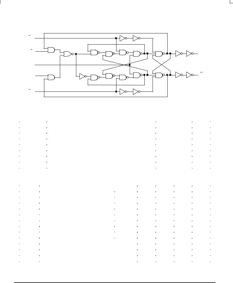
LOGIC DIAGRAM (one half shown) |
SD |
|
K |
Q |
|
|
CP |
|
J |
Q |
|
|
CD |
|
Please note that this diagram is provided only for the understanding of logic operations and should not be used to estimate propagation delays.
MAXIMUM RATINGS*
Symbol |
Parameter |
Value |
Unit |
|
|
|
|
VCC |
DC Supply Voltage (Referenced to GND) |
±0.5 to +7.0 |
V |
Vin |
DC Input Voltage (Referenced to GND) |
±0.5 to VCC +0.5 |
V |
Vout |
DC Output Voltage (Referenced to GND) |
±0.5 to VCC +0.5 |
V |
Iin |
DC Input Current, per Pin |
±20 |
mA |
Iout |
DC Output Sink/Source Current, per Pin |
±50 |
mA |
ICC |
DC VCC or GND Current per Output Pin |
±50 |
mA |
Tstg |
Storage Temperature |
±65 to +150 |
°C |
*Maximum Ratings are those values beyond which damage to the device may occur. Functional operation should be restricted to the Recommended Operating Conditions.
RECOMMENDED OPERATING CONDITIONS
Symbol |
Parameter |
|
Min |
Typ |
Max |
Unit |
|
|
|
|
|
|
|
|
|
VCC |
Supply Voltage |
′AC |
2.0 |
5.0 |
6.0 |
V |
|
|
|
|
|
||||
′ACT |
4.5 |
5.0 |
5.5 |
||||
|
|
|
|||||
|
|
|
|
|
|
|
|
Vin, Vout |
DC Input Voltage, Output Voltage (Ref. to GND) |
|
0 |
|
VCC |
V |
|
|
Input Rise and Fall Time (Note 1) |
VCC @ 3.0 V |
|
150 |
|
|
|
tr, tf |
VCC @ 4.5 V |
|
40 |
|
ns/V |
||
′AC Devices except Schmitt Inputs |
|
|
|||||
|
|
VCC @ 5.5 V |
|
25 |
|
|
|
tr, tf |
Input Rise and Fall Time (Note 2) |
VCC @ 4.5 V |
|
10 |
|
ns/V |
|
′ACT Devices except Schmitt Inputs |
VCC @ 5.5 V |
|
8.0 |
|
|||
|
|
|
|
|
|||
TJ |
Junction Temperature (PDIP) |
|
|
|
140 |
°C |
|
TA |
Operating Ambient Temperature Range |
|
±40 |
25 |
85 |
°C |
|
IOH |
Output Current Ð High |
|
|
|
±24 |
mA |
|
IOL |
Output Current Ð Low |
|
|
|
24 |
mA |
1.Vin from 30% to 70% VCC; see individual Data Sheets for devices that differ from the typical input rise and fall times.
2.Vin from 0.8 V to 2.0 V; see individual Data Sheets for devices that differ from the typical input rise and fall times.
FACT DATA
5-2
 Loading...