


Motorola MC68LC302RC16, MC68LC302RC20, MC68LC302PU20, MC68LC302CRC16, MC68LC302CRC20 Datasheet
...Microprocessors and Memory
Technologies Group
MC68LC302
Low Power Integrated
Multiprotocol Processor
Reference Manual
Motorola reserves the right to make changes without further notice to any products herein. Motorola makes no warranty, representation or guarantee regarding the suitability of its products for any particular purpose, nor does Motorola assume any liability arising out of the application or use of any product or circuit, and specifically disclaims any and all liability, including without limitation consequential or incidental damages. "Typical" parameters can and do vary in different applications. All operating parameters, including "Typicals" must be validated for each customer application by customer's technical experts. Motorola does not convey any license under its patent rights nor the rights of others. Motorola products are not designed, intended, or authorized for use as components in systems intended for surgical implant into the body, or other applications intended to support or sustain life, or for any other application in which the failure of the Motorola product could create a situation where personal injury or death may occur. Should Buyer purchase or use Motorola products for any such unintended or unauthorized application, Buyer shall indemnify and hold Motorola and its officers, employees, subsidiaries, affiliates, and distributors harmless against all claims, costs, damages, and expenses, and reasonable attorney fees arising out of, directly or indirectly, any claim of personal injury or death associated with such unintended or unauthorized use, even if such claim alleges that Motorola was negligent regarding the design or manufacture of the part. Motorola and  are registered trademarks of Motorola, Inc. Motorola, Inc. is an Equal Opportunity/Affirmative Action Employer.
Literature Distribution Centers:
USA/EUROPE: Motorola Literature Distribution; P.O. Box 20912, Arizona 85036. JAPAN: Nippon Motorola Ltd.; 4-32-1, Nishi-Gotanda, Shinagawa-ku, Tokyo 141 Japan.
ASIA-PACIFIC: Motorola Semiconductors H.K. Ltd.; Silicon Harbour Center, No. 2 Dai King Street, Tai Po Industrial Estate,
PREFACE
The complete documentation package for the MC68LC302 consists of the MC68LC302RM/ AD, MC68LC302 Low Power Integrated Multiprotocol Processor Reference Manual, M68000PM/AD, MC68000 Family Programmer’s Reference Manual, MC68302UM/AD, MC68302 Integrated Multiprotocol Processor User’s Manual, and the MC68LC302/D, MC68LC302 Low Power Integrated Multiprotocol Processor Product Brief.
The MC68LC302 Low Power Integrated Multiprotocol Processor Reference Manual describes the programming, capabilities, registers, and operation of the MC68LC302 that differ from the original MC68302; the MC68000 Family Programmer’s Reference Manual provides instruction details for the MC68LC302; and the MC68LC302 Low Power Integrated Multiprotocol Processor Product Brief provides a brief description of the MC68LC302 capabilities.
The MC68302 Integrated Multiprotocol Processor User’s Manual is required, since the MC68LC302 Low Power Integrated Multiprotocol Processor Reference Manual only describes the new features of the MC68LC302.
This user’s manual is organized as follows:
Section 1 |
Introduction |
Section 2 |
Configuration, Clocking, Low Power Modes, and Internal Memory Map |
Section 3 |
System Integration Block (SIB) |
Section 4 |
Communications Processor (CP) |
Section 5 |
Signal Description |
Section 6 |
Electrical Characteristics |
Section 7 |
Mechanical Data And Ordering Information |
ELECTRONIC SUPPORT:
The Technical Support BBS, known as AESOP (Application Engineering Support Through On-Line Productivity), can be reach by modem or the internet. AESOP provides commonly asked application questons, latest device errata, device specs, software code, and many other useful support functions.
Modem: Call 1-800-843-3451 (outside US or Canada 512-891-3650) on a modem that runs at 14,400 bps or slower. Set your software to N/8/1/F emulating a vt100.
Internet: This access is provided by telneting to pirs.aus.sps.mot.com [129.38.233.1] or through the World Wide Web at http://pirs.aus.sps.mot.com.
— Sales Offices —
For questions or comments pertaining to technical information, questions, and applications, please contact one of the following sales offices nearest you.
iii |
MC68LC302 REFERENCE MANUAL |
MOTOROLA |
UNITED STATES
ALABAMA, Huntsville |
(205) |
464-6800 |
MASSACHUSETTS, Marborough |
(508) 481-8100 |
ARIZONA, Tempe |
(602) |
897-5056 |
MASSACHUSETTS, Woburn |
(617) 932-9700 |
CALIFORNIA, Agoura Hills |
(818) |
706-1929 |
MICHIGAN, Detroit |
(313) 347-6800 |
CALIFORNIA, Los Angeles |
(310) |
417-8848 |
MINNESOTA, Minnetonka |
(612) 932-1500 |
CALIFORNIA, Irvine |
(714) |
753-7360 |
MISSOURI, St. Louis |
(314) 275-7380 |
CALIFORNIA, Rosevllle |
(916) |
922-7152 |
NEW JERSEY, Fairfield |
(201) 808-2400 |
CALIFORNIA, San Diego |
(619) |
541-2163 |
NEW YORK, Fairport |
(716) 425-4000 |
CALIFORNIA, Sunnyvale |
(408) |
749-0510 |
NEW YORK, Hauppauge |
(516) 361-7000 |
COLORADO, Colorado Springs |
(719) |
599-7497 |
NEW YORK, Poughkeepsie/Fishkill |
(914) 473-8102 |
COLORADO, Denver |
(303) |
337-3434 |
NORTH CAROLINA, Raleigh |
(919) 870-4355 |
CONNECTICUT, Wallingford |
(203) |
949-4100 |
OHIO, Cleveland |
(216) 349-3100 |
FLORIDA, Maitland |
(407) |
628-2636 |
OHIO, Columbus Worthington |
(614) 431-8492 |
FLORIDA, Pompano Beach/ |
(305) |
486-9776 |
OHIO, Dayton |
(513) 495-6800 |
Fort Lauderdal |
OKLAHOMA, Tulsa |
(800) 544-9496 |
||
FLORIDA, Clearwater |
(813) |
538-7750 |
OREGON, Portland |
(503) 641-3681 |
GEORGlA, Atlanta |
(404) |
729-7100 |
PENNSYLVANIA, Colmar |
(215) 997-1020 |
IDAHO, Boise |
(208) |
323-9413 |
Philadelphia/Horsham |
(215) 957-4100 |
ILLINOIS, Chicago/Hoffman Estates |
(708) |
490-9500 |
TENNESSEE, Knoxville |
(615) 690-5593 |
INDlANA, Fort Wayne |
(219) |
436-5818 |
TEXAS, Austin |
(512) 873-2000 |
INDIANA, Indianapolis |
(317) |
571-0400 |
TEXAS, Houston |
(800) 343-2692 |
INDIANA, Kokomo |
(317) |
457-6634 |
TEXAS, Plano |
(214) 516-5100 |
IOWA, Cedar Rapids |
(319) |
373-1328 |
VIRGINIA, Richmond |
(804) 285-2100 |
KANSAS, Kansas City/Mission |
(913) |
451-8555 |
WASHINGTON, Bellevue |
(206) 454-4160 |
MARYLAND, Columbia |
(410) |
381-1570 |
Seattle Access |
(206) 622-9960 |
|
|
|
WISCONSIN, Milwaukee/Brookfield |
(414) 792-0122 |
CANADA |
|
|
MALAYSIA, Penang |
60(4)374514 |
BRITISH COLUMBIA, Vancouver |
(604) |
293-7605 |
MEXICO, Mexico City |
52(5)282-2864 |
ONTARIO, Toronto |
(416) |
497-8181 |
MEXICO, Guadalajara |
52(36)21-8977 |
ONTARIO, Ottawa |
(613) |
226-3491 |
Marketing |
52(36)21-9023 |
QUEBEC, Montreal |
(514) |
731-6881 |
Customer Service |
52(36)669-9160 |
|
|
|
NETHERLANDS, Best |
(31)49988 612 11 |
INTERNATIONAL |
|
|
PUERTO RICO, San Juan |
(809)793-2170 |
AUSTRALIA, Melbourne |
(61-3)887-0711 |
SINGAPORE |
(65)2945438 |
|
AUSTRALIA, Sydney |
(61(2)906-3855 |
SPAIN, Madrid |
34(1)457-8204 |
|
BRAZIL, Sao Paulo |
55(11)815-4200 |
or |
34(1)457-8254 |
|
CHINA, Beijing |
86 |
505-2180 |
SWEDEN, Solna |
46(8)734-8800 |
FINLAND, Helsinki |
358-0-35161191 |
SWITZERLAND, Geneva |
41(22)7991111 |
|
Car Phone |
358(49)211501 |
SWITZERLAND, Zurich |
41(1)730 4074 |
|
FRANCE, Paris/Vanves |
33(1)40 955 900 |
TAlWAN, Taipei |
886(2)717-7089 |
|
GERMANY, Langenhagen/ Hanover |
49(511)789911 |
THAILAND, Bangkok |
(66-2)254-4910 |
|
GERMANY, Munich |
49 89 92103-0 |
UNITED KINGDOM, Aylesbury |
44(296)395-252 |
|
GERMANY, Nuremberg |
49 911 64-3044 |
FULL LINE REPRESENTATIVES |
||
GERMANY, Sindelfingen |
49 7031 69 910 |
|||
GERMANY,Wiesbaden |
49 611 761921 |
COLORADO, Grand Junction |
|
|
HONG KONG, Kwai Fong |
852-4808333 |
Cheryl Lee Whltely |
(303) 243-9658 |
|
Tai Po |
852-6668333 |
KANSAS, Wichita |
|
|
INDIA, Bangalore |
(91-812)627094 |
Melinda Shores/Kelly Greiving |
(316) 838 0190 |
|
ISRAEL, Tel Aviv |
972(3)753-8222 |
NEVADA, Reno |
|
|
ITALY, Milan |
39(2)82201 |
Galena Technology Group |
(702) 746 0642 |
|
JAPAN, Aizu |
81(241)272231 |
NEW MEXICO, Albuquerque |
|
|
JAPAN, Atsugi |
81(0462)23-0761 |
S&S Technologies, lnc. |
(505) 298-7177 |
|
JAPAN, Kumagaya |
81(0485)26-2600 |
UTAH, Salt Lake City |
|
|
JAPAN, Kyushu |
81(092)771-4212 |
Utah Component Sales, Inc. |
(801) 561-5099 |
|
JAPAN, Mito |
81(0292)26-2340 |
WASHINGTON, Spokane |
|
|
JAPAN, Nagoya |
81(052)232-1621 |
Doug Kenley |
(509) 924-2322 |
|
JAPAN, Osaka |
81(06)305-1801 |
ARGENTINA, Buenos Aires |
|
|
JAPAN, Sendai |
81(22)268-4333 |
Argonics, S.A. |
(541) 343-1787 |
|
JAPAN, Tachikawa |
81(0425)23-6700 |
HYBRID COMPONENTS RESELLERS |
||
JAPAN, Tokyo |
81(03)3440-3311 |
|||
JAPAN, Yokohama |
81(045)472-2751 |
Elmo Semiconductor |
(818) 768-7400 |
|
KOREA, Pusan |
82(51)4635-035 |
Minco Technology Labs Inc. |
(512) 834-2022 |
|
KOREA, Seoul |
82(2)554-5188 |
Semi Dice Inc. |
(310) 594-4631 |
|
MOTOROLA |
MC68LC302 REFERENCE MANUAL |
iv |
TABLE OF CONTENTS
Paragraph |
Title |
Page |
Number |
|
Number |
|
Section 1 |
|
|
Introduction |
|
1.1 |
Block Diagram......................................................................................... |
1-1 |
1.2 |
Features .................................................................................................. |
1-2 |
1.3 |
LC302 Applications ................................................................................. |
1-3 |
1.4 |
LC302 Differences .................................................................................. |
1-3 |
|
Section 2 |
|
Configuration, Clocking, Low Power Modes, and Internal Memory Map |
|
|
2.1 |
MC68LC302 and MC68302 Signal Differences ...................................... |
2-1 |
2.2 |
IMP Configuration Control....................................................................... |
2-2 |
2.2.1 |
Base Address Register ........................................................................... |
2-4 |
2.3 |
System Configuration Registers.............................................................. |
2-5 |
2.4 |
Clock Generation and Low Power Control .............................................. |
2-5 |
2.4.1 |
PLL and Oscillator Changes to IMP ........................................................ |
2-5 |
2.4.1.1 |
Clock Control Register ............................................................................ |
2-6 |
2.4.2 |
MC68LC302 System Clock Generation .................................................. |
2-6 |
2.4.2.1 |
Default System Clock Generation ........................................................... |
2-7 |
2.4.3 |
IMP System Clock Generation ................................................................ |
2-8 |
2.4.3.1 |
System Clock Configuration.................................................................... |
2-8 |
2.4.3.2 |
On-Chip Oscillator................................................................................... |
2-8 |
2.4.3.3 |
Phase-Locked Loop (PLL) ...................................................................... |
2-9 |
2.4.3.4 |
Frequency Multiplication ......................................................................... |
2-9 |
2.4.3.4.1 |
Low Power PLL Clock Divider............................................................... |
2-10 |
2.4.3.4.2 |
IMP PLL and Clock Control Register (IPLCR) ...................................... |
2-10 |
2.4.3.5 |
IMP Internal Clock Signals .................................................................... |
2-12 |
2.4.3.5.1 |
IMP System Clock................................................................................. |
2-12 |
2.4.3.5.2 |
BRG Clock ............................................................................................ |
2-12 |
2.4.3.5.3 |
PIT Clock............................................................................................... |
2-12 |
2.4.3.6 |
IMP PLL Pins ........................................................................................ |
2-12 |
2.4.3.6.1 |
VCCSYN ............................................................................................... |
2-12 |
2.4.3.6.2 |
GNDSYN............................................................................................... |
2-12 |
2.4.3.6.3 |
XFC ....................................................................................................... |
2-12 |
2.4.3.6.4 |
MODCLK............................................................................................... |
2-12 |
2.4.4 |
IMP Power Management....................................................................... |
2-13 |
2.4.4.1 |
IMP Low Power Modes ......................................................................... |
2-13 |
2.4.4.1.1 |
STOP Mode .......................................................................................... |
2-13 |
2.4.4.1.2 |
DOZE Mode .......................................................................................... |
2-13 |
2.4.4.1.3 |
STAND_BY Mode ................................................................................. |
2-13 |
MOTOROLA |
MC68LC302 REFERENCE MANUAL |
v |
Table of Contents |
|
||
Paragraph |
|
Title |
Page |
Number |
|
|
Number |
2.4.4.1.4 |
SLOW_GO Mode................................................................................... |
2-14 |
|
2.4.4.1.5 |
NORMAL Mode...................................................................................... |
2-14 |
|
2.4.4.1.6 |
IMP Operation Mode Control Register (IOMCR) |
...................................2-14 |
|
2.4.4.1.7 |
Low Power Drive Control Register (LPDCR) ......................................... |
2-15 |
|
2.4.4.1.8 |
IMP Power Down Register (IPWRD) ..................................................... |
2-15 |
|
2.4.4.1.9 |
Default Operation Modes. ...................................................................... |
2-15 |
|
2.4.4.2 |
Low Power Support................................................................................ |
2-15 |
|
2.4.4.2.1 |
Enter the SLOW_GO mode ................................................................... |
2-15 |
|
2.4.4.2.2 |
Entering the STOP/ DOZE/ STAND_BY Mode...................................... |
2-16 |
|
2.4.4.2.3 |
IMP Wake-Up from Low Power STOP Modes ....................................... |
2-17 |
|
2.4.4.2.4 |
IMP Wake-Up Control Register (IWUCR) .............................................. |
2-17 |
|
2.4.4.3 |
Fast Wake-Up ........................................................................................ |
2-18 |
|
2.4.4.3.5 |
Ring Oscillator Control Register (RINGOCR) ........................................ |
2-19 |
|
2.4.4.3.6 |
Ring Oscillator Event Register (RINGOEVR). ....................................... |
2-20 |
|
2.5 |
MC68LC302 Dual Port RAM.................................................................. |
2-20 |
|
2.6 |
Internal Registers map........................................................................... |
2-23 |
|
|
Section 3 |
|
|
System Integration Block (SIB) |
|
3.1 |
System Control ........................................................................................ |
3-1 |
3.1.1 |
System Control Register (SCR) ............................................................... |
3-2 |
3.1.2 |
System Status Bits................................................................................... |
3-3 |
3.1.3 |
System Control Bits ................................................................................. |
3-3 |
3.1.4 |
Freeze Control ......................................................................................... |
3-5 |
3.1.5 |
Hardware Watchdog ................................................................................ |
3-5 |
3.2 |
Programmable Data Bus Size Switch ...................................................... |
3-6 |
3.2.1 |
Bus Switch Register (BSR) ...................................................................... |
3-6 |
3.2.2 |
Basic Procedure:...................................................................................... |
3-6 |
3.3 |
Load Boot Code from An SCC................................................................. |
3-7 |
3.4 |
DMA Control .......................................................................................... |
3-10 |
3.4.1 |
MC68LC302 Differences........................................................................ |
3-10 |
3.4.2 |
IDMA Registers (Independent DMA Controller)..................................... |
3-11 |
3.4.2.1 |
Channel Mode Register (CMR).............................................................. |
3-11 |
3.4.2.2 |
Source Address Pointer Register (SAPR) ............................................. |
3-13 |
3.4.2.3 |
Destination Address Pointer Register (DAPR)....................................... |
3-13 |
3.4.2.4 |
Function Code Register (FCR) .............................................................. |
3-13 |
3.4.2.5 |
Byte Count Register (BCR).................................................................... |
3-13 |
3.4.2.6 |
Channel Status Register (CSR) ............................................................. |
3-13 |
3.5 |
Interrupt Controller ................................................................................. |
3-14 |
3.5.1 |
Interrupt Controller Key Differences....................................................... |
3-14 |
3.5.2 |
Interrupt Controller Programming Model................................................ |
3-14 |
3.5.2.1 |
Global Interrupt Mode Register (GIMR) ................................................. |
3-14 |
3.5.2.2 |
Interrupt Pending Register (IPR)............................................................ |
3-15 |
3.5.2.3 |
Interrupt Mask Register (IMR)................................................................ |
3-16 |
3.5.2.4 |
Interrupt In-Service Register (ISR)......................................................... |
3-16 |
vi |
MC68LC302 REFERENCE MANUAL |
MOTOROLA |
|
|
|
Table of Contents |
Paragraph |
Title |
Page |
|
Number |
|
|
Number |
3.6 |
Parallel I/O Ports ................................................................................... |
3-17 |
|
3.6.1 |
Parallel I/O Port Differences.................................................................. |
3-17 |
|
3.6.2 |
Port A .................................................................................................... |
3-17 |
|
3.6.3 |
Port B .................................................................................................... |
3-18 |
|
3.6.3.1 |
PB7–PB3............................................................................................... |
3-18 |
|
3.6.3.2 |
PB11–PB8............................................................................................. |
3-18 |
|
3.6.4 |
Port N .................................................................................................... |
3-19 |
|
3.6.5 |
Port Registers........................................................................................ |
3-19 |
|
3.7 |
Timers ................................................................................................... |
3-20 |
|
3.7.1 |
MC68LC302 General Purpose Timer Difference .................................. |
3-20 |
|
3.7.2 |
General Purpose Timers Programming Mode....................................... |
3-20 |
|
3.7.2.1 |
Timer Mode Register (TMR1, TMR2).................................................... |
3-20 |
|
3.7.2.2 |
Timer Reference Registers (TRR1, TRR2) ........................................... |
3-21 |
|
3.7.2.3 |
Timer Capture Registers (TCR1, TCR2) ............................................... |
3-21 |
|
3.7.2.4 |
Timer Counter (TCN1, TCN2) ............................................................... |
3-21 |
|
3.7.2.5 |
Timer Event Registers (TER1, TER2) ................................................... |
3-21 |
|
3.7.3 |
Timer 3 - Software Watchdog Timer ..................................................... |
3-22 |
|
3.7.3.1 |
Software Watchdog Reference Register (WRR) ................................... |
3-22 |
|
3.7.3.2 |
Software Watchdog Counter (WCN) ..................................................... |
3-22 |
|
3.7.4 |
Periodic Interrupt Timer (PIT)................................................................ |
3-22 |
|
3.7.4.1 |
Overview ............................................................................................... |
3-23 |
|
3.7.4.2 |
Periodic Timer Period Calculation ......................................................... |
3-23 |
|
3.7.4.3 |
Using the Periodic Timer As a Real-Time Clock ................................... |
3-24 |
|
3.7.4.4 |
Periodic Interrupt Timer Register (PITR)............................................... |
3-24 |
|
3.8 |
External Chip-Select Signals and Wait-State Logic .............................. |
3-25 |
|
3.8.1 |
Chip-Select Registers............................................................................ |
3-26 |
|
3.8.1.1 |
Base Register (BR3–BR0) .................................................................... |
3-26 |
|
3.8.1.2 |
Option Registers (OR3–OR0) ............................................................... |
3-26 |
|
3.8.2 |
Disable CPU Logic (M68000)................................................................ |
3-28 |
|
3.8.3 |
Bus Arbitration Logic ............................................................................. |
3-28 |
|
3.8.3.1 |
Internal Bus Arbitration.......................................................................... |
3-28 |
|
3.8.3.2 |
External Bus Arbitration......................................................................... |
3-28 |
|
3.9 |
Dynamic RAM Refresh Controller ......................................................... |
3-29 |
|
|
Section 4 |
|
|
|
Communications Processor (CP) |
|
|
4.1 |
MC68LC302 Key Differences from the MC68302 ................................... |
4-1 |
|
4.2 |
Serial Channels Physical Interface.......................................................... |
4-2 |
|
4.2.1 |
Serial Interface Registers ........................................................................ |
4-2 |
|
4.2.1.1 |
Serial Interface Mode Register (SIMODE) .............................................. |
4-2 |
|
4.2.1.2 |
Serial Interface Mask Register (SIMASK) ............................................... |
4-4 |
|
4.3 |
Serial Communication Controllers (SCCs) .............................................. |
4-4 |
|
4.3.1 |
SCC Configuration Register (SCON) ...................................................... |
4-4 |
|
4.3.1.1 |
Divide by 2 Input Blocks (New Feature) .................................................. |
4-4 |
|
4.3.2 |
Disable SCC1 Serial Clocks Out (DISC) ................................................. |
4-4 |
|
4.3.2.1 |
RCLK1 and TCLK1 Pin Options .............................................................. |
4-5 |
|
MOTOROLA |
MC68LC302 REFERENCE MANUAL |
vii |
|
Table of Contents |
|
||
Paragraph |
|
Title |
Page |
Number |
|
|
Number |
4.3.3 |
SCC Mode Register (SCM)...................................................................... |
4-5 |
|
4.3.4 |
SCC Data Synchronization Register (DSR)............................................. |
4-6 |
|
4.3.5 |
Buffer Descriptors Table .......................................................................... |
4-6 |
|
4.3.6 |
SCC Parameter RAM Memory Map......................................................... |
4-7 |
|
4.3.7 |
Interrupt Mechanism ................................................................................ |
4-7 |
|
4.3.8 |
UART Controller....................................................................................... |
4-7 |
|
4.3.8.1 |
UART Memory Map ................................................................................. |
4-7 |
|
4.3.8.2 |
UART Mode Register............................................................................... |
4-8 |
|
4.3.8.3 |
UART Receive Buffer Descriptor (Rx BD) ............................................... |
4-8 |
|
4.3.8.4 |
UART Transmit Buffer Descriptor (Tx BD)............................................... |
4-8 |
|
4.3.8.5 |
UART Event Register............................................................................... |
4-9 |
|
4.3.8.6 |
UART MASK Register.............................................................................. |
4-9 |
|
4.3.9 |
Autobaud Controller (New) ...................................................................... |
4-9 |
|
4.3.9.1 |
Autobaud Channel Reception Process .................................................... |
4-9 |
|
4.3.9.2 |
Autobaud Channel Transmit Process .................................................... |
4-11 |
|
4.3.9.3 |
Autobaud Parameter RAM..................................................................... |
4-11 |
|
4.3.9.4 |
Autobaud Programming Model .............................................................. |
4-13 |
|
4.3.9.4.1 |
Preparing for the Autobaud Process...................................................... |
4-13 |
|
4.3.9.4.2 |
Enter_Baud_Hunt Command................................................................. |
4-14 |
|
4.3.9.4.3 |
Autobaud Command Descriptor............................................................. |
4-14 |
|
4.3.9.4.4 |
Autobaud Lookup Table......................................................................... |
4-15 |
|
4.3.9.5 |
Lookup Table Example .......................................................................... |
4-17 |
|
4.3.9.6 |
Determining Character Length and Parity.............................................. |
4-17 |
|
4.3.9.7 |
Autobaud Reception Error Handling Procedure..................................... |
4-18 |
|
4.3.9.8 |
Autobaud Transmission ......................................................................... |
4-18 |
|
4.3.9.8.1 |
Automatic Echo...................................................................................... |
4-19 |
|
4.3.9.8.2 |
Smart Echo ............................................................................................ |
4-19 |
|
4.3.9.9 |
Reprogramming to UART Mode or Another Protocol ............................ |
4-20 |
|
4.3.10 |
HDLC Controller..................................................................................... |
4-20 |
|
4.3.10.1 |
HDLC Memory Map ............................................................................... |
4-20 |
|
4.3.10.2 |
HDLC Mode Register............................................................................. |
4-20 |
|
4.3.10.3 |
HDLC Receive Buffer Descriptor (Rx BD) ............................................. |
4-21 |
|
4.3.10.4 |
HDLC Transmit Buffer Descriptor (Tx BD)............................................. |
4-21 |
|
4.3.10.5 |
HDLC Event Register............................................................................. |
4-21 |
|
4.3.10.6 |
HDLC Mask Register ............................................................................. |
4-21 |
|
4.3.11 |
BISYNC Controller ................................................................................. |
4-22 |
|
4.3.11.1 |
BISYNC Memory Map............................................................................ |
4-22 |
|
4.3.11.2 |
BISYNC Mode Register ......................................................................... |
4-22 |
|
4.3.11.3 |
BISYNC Receive Buffer Descriptor (Rx BD).......................................... |
4-22 |
|
4.3.11.4 |
BISYNC Transmit Buffer Descriptor (Tx BD). ........................................ |
4-22 |
|
4.3.11.5 |
BISYNC Event Register ......................................................................... |
4-23 |
|
4.3.11.6 |
BISYNC Mask Register.......................................................................... |
4-23 |
|
4.3.12 |
Transparent Controller ........................................................................... |
4-23 |
|
4.3.12.1 |
Transparent Memory Map...................................................................... |
4-23 |
|
4.3.12.2 |
Transparent Mode Register ................................................................... |
4-24 |
|
viii |
MC68LC302 REFERENCE MANUAL |
MOTOROLA |
|
|
|
Table of Contents |
Paragraph |
Title |
Page |
|
Number |
|
|
Number |
4.3.12.3 |
Transparent Receive Buffer Descriptor (RxBD) .................................... |
4-24 |
|
4.3.12.4 |
Transparent Transmit Buffer Descriptor (Tx BD)................................... |
4-25 |
|
4.3.12.5 |
Transparent Event Register .................................................................. |
4-25 |
|
4.3.12.6 |
Transparent Mask Register ................................................................... |
4-25 |
|
4.4 |
Serial Communication Port (SCP)......................................................... |
4-25 |
|
4.4.1 |
SCP Programming Model...................................................................... |
4-25 |
|
4.4.2 |
SCP Transmit/Receive Buffer Descriptor .............................................. |
4-26 |
|
4.5 |
Serial Management Controllers (SMCs)................................................ |
4-26 |
|
4.5.1 |
SMC Programming Model ..................................................................... |
4-26 |
|
4.5.2 |
SMC Memory Structure and Buffers Descriptors .................................. |
4-26 |
|
4.5.2.1 |
SMC1 Receive Buffer Descriptor .......................................................... |
4-26 |
|
4.5.2.2 |
SMC1 Transmit Buffer Descriptor ......................................................... |
4-26 |
|
4.5.2.3 |
SMC2 Receive Buffer Descriptor .......................................................... |
4-27 |
|
4.5.2.4 |
SMC2 Transmit Buffer Descriptor ......................................................... |
4-27 |
|
|
Section 5 |
|
|
|
Signal Description |
|
|
5.1 |
Functional Groups ................................................................................... |
5-1 |
|
5.2 |
Power Pins .............................................................................................. |
5-2 |
|
5.3 |
Clock Pins ............................................................................................... |
5-4 |
|
5.4 |
System Control Pins................................................................................ |
5-5 |
|
5.5 |
Address Bus Pins (A19–A1).................................................................... |
5-7 |
|
5.6 |
Data Bus Pins (D15—D0) ....................................................................... |
5-8 |
|
5.7 |
Bus Control Pins...................................................................................... |
5-9 |
|
5.8 |
Bus Arbitration Pins............................................................................... |
5-10 |
|
5.9 |
Interrupt Control Pins ............................................................................ |
5-11 |
|
5.10 |
MC68LC302 Bus Interface Signal Summary......................................... |
5-12 |
|
5.11 |
Physical Layer Serial Interface Pins...................................................... |
5-14 |
|
5.12 |
Typical Serial Interface Pin Configurations ........................................... |
5-14 |
|
5.13 |
NMSI1 or ISDN Interface Pins............................................................... |
5-14 |
|
5.14 |
NMSI2 Port or Port a Pins ..................................................................... |
5-17 |
|
5.15 |
PAIO / SCP Pins ................................................................................... |
5-18 |
|
5.16 |
Timer Pins ............................................................................................. |
5-19 |
|
5.17 |
Parallel I/O Pins with Interrupt Capability .............................................. |
5-20 |
|
5.18 |
Chip-Select Pins.................................................................................... |
5-21 |
|
5.19 |
When to Use Pullup Resistors............................................................... |
5-21 |
|
|
Section 6 |
|
|
|
Electrical Characteristics |
|
|
6.1 |
Maximum Ratings.................................................................................... |
6-2 |
|
6.2 |
Thermal Characteristics .......................................................................... |
6-2 |
|
6.3 |
Power Considerations ............................................................................. |
6-3 |
|
6.4 |
Power Dissipation.................................................................................... |
6-4 |
|
6.5 |
DC Electrical Characteristics................................................................... |
6-5 |
|
6.6 |
DC Electrical Characteristics—NMSI1 in IDL Mode................................ |
6-6 |
|
6.7 |
AC Electrical Specifications—Clock Timing ............................................ |
6-6 |
|
MOTOROLA |
MC68LC302 REFERENCE MANUAL |
ix |
|
Table of Contents |
|
|
Paragraph |
Title |
Page |
Number |
|
Number |
6.7.1AC Electrical Characteristics - IMP Phased Lock Loop (PLL)
|
Characteristics ......................................................................................... |
6-7 |
6.8 |
AC Electrical Specifications—IMP Bus Master Cycles ............................ |
6-8 |
6.9 |
AC Electrical Specifications—DMA ....................................................... |
6-13 |
6.10AC Electrical Specifications—External Master
Internal Asynchronous Read/Write Cycles ............................................ |
6-16 |
6.11AC Electrical Specifications—External Master Internal Synchronous
Read/Write Cycles ................................................................................. |
6-19 |
6.12AC Electrical Specifications—Internal Master Internal Read/Write
|
Cycles .................................................................................................... |
6-23 |
6.13 |
AC Electrical Specifications—Chip-Select Timing Internal Master ....... |
6-24 |
6.14 |
AC Electrical Specifications—Chip-Select Timing External Master ....... |
6-25 |
6.15 |
AC Electrical Specifications—Parallel I/O ............................................. |
6-26 |
6.16 |
AC Electrical Specifications—Interrupts ............................................... |
6-26 |
6.17 |
AC Electrical Specifications—Timers..................................................... |
6-28 |
6.18 |
AC Electrical Specifications—Serial Communications Port ................... |
6-29 |
6.19 |
AC Electrical Specifications—IDL Timing) ............................................. |
6-30 |
6.20 |
AC Electrical Specifications—GCI Timing ............................................. |
6-32 |
6.21 |
AC Electrical Specifications—PCM Timing............................................ |
6-34 |
6.22 |
AC Electrical Specifications—NMSI Timing........................................... |
6-36 |
|
Section 7 |
|
|
Mechanical Data and Ordering Information |
|
7.1 |
Pin Assignments ...................................................................................... |
7-1 |
7.1.1 |
Pin Grid Array (PGA) ............................................................................... |
7-1 |
7.1.2 |
Surface Mount (TQFP )............................................................................ |
7-2 |
7.2 |
Package Dimensions ............................................................................... |
7-3 |
7.2.1 |
Pin Grid Array (PGA) ............................................................................... |
7-3 |
7.2.2 |
Surface Mount (TQFP)............................................................................. |
7-4 |
7.3 |
Ordering Information ................................................................................ |
7-5 |
x |
MC68LC302 REFERENCE MANUAL |
MOTOROLA |

SECTION 1
INTRODUCTION
Motorola has developed a low-cost version of the well-known MC68302 integrated multiprotocol processor (IMP) called the MC68LC302. Simply put, the LC302 is a traditional 68302 minus the third serial communication controller (SCC3) and has a new static 68000 core, a new timer and low power modes. It is packaged in a low profile 100 TQFP that reduces board space from the regular 68302, as well as making it suitable for use in height restricted applications such as PCMCIA.
The document fully describes all the differences between the LC302 and the regular 68302. Any feature not described in this document will operate as described in the MC68302 User’s Manual. In addition this document contains the full set of electrical descriptions for the LC302, even though most of them are exactly the same as the 68302.
1.1 BLOCK DIAGRAM
The block diagram is shown in Figure 1-1.
LOW |
|
1 GENERAL- |
|
3 TIMERS |
|
POWER |
INTERRUPT |
PURPOSE |
4 CHIP SELECTS |
RAM / ROM |
|
CONTROL |
CONTROLLER |
DMA |
|
PIO |
|
|
|
||||
|
|
CHANNEL |
SYSTEM CONTROL |
|
|
STATIC |
|
|
68000 |
|
|
|
SYSTEM BUS |
|
|
||
M68000 |
|
|
|
||
|
|
|
|
20 ADDRESS |
|
CORE |
|
|
|
|
|
|
|
|
|
|
8/16 DATA |
|
|
4 SDMA |
1152 BYTES |
PIT |
|
|
|
DUAL-PORT |
|
||
|
|
CHANNELS |
|
|
|
|
|
RAM |
|
|
|
|
|
|
|
|
|
RISC |
|
PERIPHERAL BUS |
|
|
|
CONTROLLER |
|
|
|
|
|
|
|
2 SERIAL |
SCP |
|
|
|
|
CHANNELS |
+ |
|
|
|
|
(SCCs) |
2 SMCs |
|
|
68LC302
Figure 1-1. MC68LC302 Block Diagram
MOTOROLA |
MC68LC302 REFERENCE MANUAL |
1-1 |
Introduction
1.2 FEATURES
The features of the LC302 are as follows. The items in bold face type show major differences from the MC68302, although a complete list of differences is given in 1.4 LC302 Differences.
•On-Chip Static 68000 Core Supporting a 16or 8-Bit M68000 Family-System
•SIB Including:
Independent Direct Memory Access (IDMA) Controller.
Interrupt Controller with Two Modes of Operation
Parallel Input/Output (I/O) Ports, some with Interrupt Capability
Parallel Input/Output (I/O) Ports on D15-D8 in 8 bit mode
On-Chip 1152-Byte Dual-Port RAM
Three Timers Including a Watchdog Timer
New Periodic Interrupt Timer (PIT)
Four Programmable Chip-Select Lines with Wait-State Generator Logic Programmable Address Mapping of the Dual-Port RAM and IMP Registers On-Chip Clock Generator with Output Signal
On-Chip PLL Allows Operation with 32kHz or 4MHz Crystals Glueless Interface to EPROM, SRAM, Flash EPROM, and EEPROM Allows Boot in 8-bit Mode, and Running Switch to 16-bit Mode
System Control:
System Status and Control Logic
Disable CPU Logic (Slave Mode Operation) Hardware Watchdog
New Low-Power (Standby) Modes With Wake-up From 2 Pins or PIT
Freeze Control for Debugging (Available Only in the PGA Package) DRAM Refresh Controller
• CP Including:
Main Controller (RISC Processor)
Two Independent Full-Duplex Serial Communications Controllers (SCCs)
Supporting Various Protocols:
High-Level/Synchronous Data Link Control (HDLC/SDLC)
Universal Asynchronous Receiver Transmitter (UART)
Binary Synchronous Communication (BISYNC)
Transparent Modes
Autobaud Support Instead of DDCMP and V.110
Boot from SCC Capability
1-2 |
MC68LC302 REFERENCE MANUAL |
MOTOROLA |

Introduction
Four Serial DMA Channels for the Two SCCs
Flexible Physical Interface Accessible by SCCs Including:
Motorola Interchip Digital Link (IDL)
General Circuit Interface (GCI, Also Known as IOM1-2)
Pulse Code Modulation (PCM) Highway Interface
Nonmultiplexed Serial Interface (NMSI) Implementing Standard
Modem Signals
SCP for Synchronous Communication
Two Serial Management Controllers (SMCs) To Support IDL and GCI Auxiliary Channels
• 100 Pin Thin Quad Flat Pack (TQFP) Packaging
1.3 LC302 APPLICATIONS
The LC302 excels in several applications areas.
First, any application using the 68302, but not needing all three serial channels is a potential candidate for the LC302. Note however, that the LC302 sacrifices most of the provision for external bus mastership, thus the LC302 may not be appropriate where the 68302 is used as part of larger systems.
Second, the LC302 excels in low power and portable applications. The inclusion of a static 68000 core coupled with the low power modes built into the device make it ideal for handheld, or other low power applications. The new 32 kHz or 4 MHz PLL option greatly reduces the total power budget of the designer’s board, and allows the LC302 to be an effective device in low power systems. The LC302 can then optionally generate a full frequency clock for use by the rest of the board. During low power modes, the new periodic interrupt timer (PIT) allows the device to be woken up at regular intervals. In addition, two pins allow the device to be woken up from low power modes.
Third, given that the LC302 is packaged in a 100TQFP package, it allows the 68302 to be used in space critical applications, as well as height critical applications such as PCMCIA cards.
Fourth, since the disable CPU mode (also known as slave mode) is still retained, the LC302 can function as a fully intelligent DMA-driven peripheral chip containing serial channels, timers, and chip selects, etc.
1.4 LC302 DIFFERENCES
The LC302 has some specific differences from the 68302. Most of these differences simply result from the reduction in pins from 132 on the original 68302, to 100 pins on the LC302.
1. IOMisatrademarkofSiemensAG
MOTOROLA |
MC68LC302 REFERENCE MANUAL |
1-3 |

Introduction
The following features have been removed or modified from the 68302 in order to make the LC302 possible.
•SCC3 and its baud rate generator (BRG3) are removed.
•External masters are not able to take the bus away from the LC302 except through a simple scheme using the HALT pin. This restriction does not apply to using the LC302 in CPU disabled mode (slave mode), in which case BR, BG, and BGACK are all available (they replace the IPL2-0 pins).
•Although the Independent DMA (IDMA) is still available, the external IDMA request pins (DREQ, DACK, and DONE) have been eliminated.
•Four address lines have been eliminated, giving a total of 20 address lines. However, the LC302 supports more than a 1 MB addressing range, since each of the four chip selects still decodes a 24-bit address. This allows a total of 4 MB to be addressed.
•Since the function code pins and AVEC have been removed, interrupt acknowledgment to external devices is only provided on levels one, six, and seven.
•The DDCMP and V.110 protocols have been removed.
•The total list of pins removed is: A23-A20, FC2-FC0† , AVEC† , RMC, IAC† , BERR, BR, BG, BGACK, BCLR, IACK1, IACK6, IACK7, DREQ, DACK, DONE, BRG1, FRZ† , TOUT1, NC1, NC3, TCLK3, RTS3, CTS3, CD3, plus 5 power and ground pins.
NOTE
Signals marked with † are available in the PGA Package.
•The SCP pins are now muxed with PA8, PA9, and PA10. The TXD3, RXD3, and RCLK3 functions associated with SCC3 are eliminated.
•The UDS, LDS, and R/W pins are not available except in slave mode, where they replace the WEH, WEL, and OE pins. Instead, the new pins WEH, WEL, and OE have been defined for glueless interfacing to memory.
•PA12 is now muxed with the MODCLK pin, which is associated with the 32 kHz or 4 MHz PLL. The MODCLK pin is sampled after reset, and then becomes PA12.
•New VCCsyn, GNDsyn, and XFC pins have been added in support of the on-chip PLL.
•For purposes of emulation support only, a special 132 PGA version is supported. This version adds back the FC2-0, IAC, FRZ, and AVEC pins. The FC2-0 pins allow bus cycles to be distinguished between program and data accesses, interrupt cycles, etc. The IAC, FRZ, and AVEC pins are provided so that emulation vendors can quickly retrofit their existing 68302 emulator designs to support the LC302.
1-4 |
MC68LC302 REFERENCE MANUAL |
MOTOROLA |

SECTION 2
CONFIGURATION, CLOCKING, LOW POWER MODES, AND INTERNAL MEMORY MAP
The MC68LC302 integrates a high-s/peed M68000 processor with multiple communications peripherals. The provision of direct memory access (DMA) control and link layer management with the serial ports allows high throughput of data for communications-intensive applications, such as basic rate Integrated Services Digital Network (ISDN).
The MC68LC302 can operate either in the full MC68000 mode with a 16-bit data bus or in the MC68008 mode with an 8-bit data bus by connecting the bus width (BUSW) pin low.
NOTE
The BUSW pin is static and is not intended to be used for dynamic bus sizing. Instead the BSW and BSWEN bits in the BSR register should be used to switch the bus width after reset (3.2 Programmable Data Bus Size Switch). If the state of the BUSW pin is changed during operation of the MC68LC302, erratic operation may occur.
Refer to the MC68000UM/AD, M68000 8-/16-/32-Bit Microprocessors User's Manual, and the MC68302UM/AD, MC68302 Integrated Multiprotocol Processor User’s Manual, for complete details of the on-chip microprocessor including the programming model and instruction set summary. Throughout this manual, references may use the notation M68000, meaning all devices belonging to this family of microprocessors, or the notation MC68000, MC68008, meaning the specific microprocessor products.
This section is intended to describe configuration of the MC68LC302 and the differences between theLC302 and the MC68000 and the MC68302.This section also includes tables that show the registers of the IMP portion of the MC68LC302. All of the registers are memory mapped into the 68000 space
2.1 MC68LC302 AND MC68302 SIGNAL DIFFERENCES
The MC68LC302 in CPU enable mode has Write Enable (WE) signals instead of UDS and LDS signal. The Write Enable High (WEH/A0) signal indicates that most significant data byte will be accessed, and the Write Enable Low (WEL/DS) indicates that the least significant data byte will be accessed. When the core is disabled, WEH/A0 and WEL/DS become UDS/ A0 and LDS/DS respectively.
MOTOROLA |
MC68LC302 REFERENCE MANUAL |
2-1 |

Configuration, Clocking, Low Power Modes, and Internal Memory Map
The MC68LC302 in CPU enable mode has an output enable (OE) signal instead of R/W. The OE signal indicates that the MC68LC302 expects an external device to drive data onto the data bus. When the core is disabled, OE becomes the R/W signal.
The MC68LC302 in CPU enable mode does not have BR, BG, and BGACK pins. Instead the HALT pin is used to force the MC68LC302 off of the bus (see the HALT signal description in 5.4 System Control Pins). While the MC68LC302 is halted, the chip selects are still functional. The external master will not be able to access the internal registers and dual-port RAM.
When the core is disabled, the IPL0, IPL1, and IPL2 lines become the BR, BG, and BGACK signals. The only external interrupts handled are PB8, PB9, PB10, and PB11.
Two M6800 signals are omitted from the 68LC302: valid memory address (VMA) and enable
(E). The valid peripheral address (VPA) signal which was used on the MC68302 as AVEC has been removed from the MC68LC302.
The signals for the serial communications port (SCP) have been multiplexed with the PA8, PA9, and PA10 pins and the signals for SCC3 have been removed.
The FC2-0 pins have been removed from the MC68LC302. These signals are still driven internally by the core depending on the type of bus cycle (i.e. supervisor program space, supervisor data space, etc.) and the internal peripherals. They can still be used for address comparison in the chip select registers. In disable CPU mode and when HALT is asserted for external masters, the FC signals are internally driven to 5 for external master accesses to internal peripherals.
The A23-A20 pins have been removed from the MC68LC302. These signals are still driven internally by the core and the internal peripherals. The user must program the full 24-bit address in the chip select base registers, option registers, and in the pointers used by the internal DMA and SCCs. In disable CPU mode and when HALT is asserted for external masters, the A23-20 signals are driven to zero for all external master accesses.
The other signals removed from the MC68LC302 are IAC, RMC, BLCR, BERR, FRZ, BRG1, DREQ/PA13, DACK/PA14, DONE/PA15, IACK7/PB0, IACK6/PB1, IACK7/PB2, and TOUT1/PB4.
The signals XFC and MODCLK (multiplexed with PA12) have been added for use with the on-chip phase lock loop.
For purposes of emulation support only, a special 132 PGA version is supported. This version adds back the FC2-0, IAC, FRZ, and AVEC pins.
2.2 IMP CONFIGURATION CONTROL
A number of reserved entries in the external M68000 exception vector table are used as addresses for the internal system configuration registers. See Table 2-1.
2-2 |
MC68LC302 REFERENCE MANUAL |
MOTOROLA |

Configuration, Clocking, Low Power Modes, and Internal Memory Map
The BAR entry contains the BAR described in this section. The SCR entry contains the SCR described in Section 3 System Integration Block (SIB).
Figure 2-1 shows all the IMP on-chip addressable locations and how they are mapped into system memory.
|
|
|
SYSTEM MEMORY MAP |
||
|
|
|
$0 |
|
|
|
IMP |
EXCEPTION |
|
||
|
|
|
|||
|
|
|
|
VECTOR |
|
|
|
|
|
TABLE |
|
$0F0 |
PITR |
|
|
|
|
|
|
|
|
||
|
|
|
|
||
|
|
|
|
|
|
$0F2 |
BAR ENTRY |
|
|
256 VECTOR |
|
$0F4 |
SCR ENTRY |
|
$3FF |
ENTRIES |
|
|
|
|
|||
$0F7 |
|
|
|
|
|
WAKE-UP |
|
|
|
|
|
|
|
|
|
|
|
$0F8 |
IMP PLL |
|
|
|
|
$0FA |
|
|
BAR |
|
|
IMP MODE CONTROL |
|
|
|
||
|
POINTS |
|
|
||
$0FB |
|
|
TO THE |
|
|
IMP POWER DOWN |
|
|
|
||
|
BASE |
|
|
||
|
|
|
|
|
|
|
4K BLOCK |
|
|
|
|
BASE + $0 |
|
|
|
|
|
SYSTEM RAM |
|
|
|
|
|
|
|
|
|
|
|
|
(DUAL-PORT) |
|
$xxx000 = BASE |
|
|
|
|
|
|
|
|
BASE + $400 |
|
|
|
4K BLOCK |
|
PARAMETER RAM |
|
|
|
|
|
|
|
|
|
|
|
|
|
|
|
|
|
|
(DUAL-PORT) |
|
|
|
|
BASE + $800 |
|
|
|
|
|
INTERNAL |
|
|
|
|
|
|
|
|
|
|
|
|
REGISTERS |
|
|
|
|
BASE + $FFF |
|
|
$FFFFFF |
|
|
|
|
|
|
|
|
Figure 2-1. IMP Configuration Control
The on-chip peripherals, including those peripherals in both the communications processor (CP) and system integration block (SIB), require a 4K-byte block of address space. This 4Kbyte block location is determined by writing the intended base address to the BAR in supervisor data space (FC = 5). The FC2-0 pins are internally driven by the MC68LC302 to supervisor data space.
After a total system reset, the on-chip peripheral base address is undefined, and it is not possible to access the on-chip peripherals at any address until BAR is written. The BAR and the SCR can always be accessed at their fixed addresses.
NOTE
The BAR and SCR registers are internally reset only when a total system reset occurs by the simultaneous assertion of RESET
MOTOROLA |
MC68LC302 REFERENCE MANUAL |
2-3 |

Configuration, Clocking, Low Power Modes, and Internal Memory Map
and HALT. The chip-select (CS) lines are not asserted on accesses to these locations. Thus, it is very helpful to use CS lines to select external ROM/RAM that overlaps the BAR and SCR register locations, since this prevents potential bus contention.
NOTE
In 8-bit system bus operation, IMP accesses are not possible until the low byte of the BAR is written. Since the MOVE.W instruction writes the high byte followed by the low byte, this instruction guarantees the entire word is written.
Do not assign other devices on the system bus an address that falls within the address range of the peripherals defined by the BAR. If this happens, an internal BERR is generated to the core (if the address decode conflict enable (ADCE) bit is set) and the address decode conflict (ADC) bit in the SCR is set.
2.2.1 Base Address Register
The BAR is a 16-bit, memory-mapped, read-write register consisting of the high address bits, the compare function code bit, and the function code bits. Upon a total system reset, its value may be read as $BFFF, but its value is not valid until written by the user. The address of this register is fixed at $0F2 in supervisor data space. BAR cannot be accessed in user data space.
15 |
13 |
12 |
11 |
|
|
|
|
|
|
|
|
|
|
|
0 |
|
FC2–FC0 |
CFC |
|
|
|
|
|
BASE ADDRESS |
|
|
|
|
|
||
|
|
|
|
|
|
|
|
|
|
|
|
|
|
||
|
23 |
22 |
21 |
20 |
19 |
|
18 |
17 |
16 |
15 |
14 |
13 |
12 |
||
|
|
|
|
||||||||||||
|
|
|
|
|
|
|
|
|
|
|
|
|
|
|
|
Bits 15–13—FC2–FC0
The FC2–FC0 field is contained in bits 15–13 of the BAR. These bits are used to set the address space of 4K-byte block of on-chip peripherals. The address compare logic uses these bits, dependent upon the CFC bit, to cause an address match within its address space. When the core is enabled, the function code bits will be driven by the core to indicate the type of cycle in process. In disable CPU mode, the FC pins are not present and are internally driven to 5. Since, the user does not have any control over how the FC signals are driven, it is recommended that the user write these bits to zero and write the CFC bit to zero to disable the FC comparison.
NOTE
Do not assign this field to the M68000 core interrupt acknowledge space (FC2–FC0 = 7).
CFC—Compare Function Code
0 = The FC bits in the BAR are ignored. Accesses to the IMP 4K-byte block occur without comparing the FC bits.
1 = The FC bits in the BAR are compared. The address space compare logic uses the FC bits to detect address matches.
2-4 |
MC68LC302 REFERENCE MANUAL |
MOTOROLA |

Configuration, Clocking, Low Power Modes, and Internal Memory Map
Bits 11–0—Base Address
The high address field is contained in bit 11–0 of the BAR. These bits are used to set the starting address of the dual-port RAM. The address compare logic uses only the most significant bits to cause an address match within its block size. Even though A23-20 are signals are not available, they are driven internally by the core, or driven to zeroes in disable CPU mode or when HALT has been asserted by an external master.
2.3 SYSTEM CONFIGURATION REGISTERS
A number of entries in the M68000 exception vectors table (located in low RAM) are reserved for the addresses of system configuration registers (see Table 2-1). These registers have seven addresses within $0F0-$0FF. The MC68LC302 uses one of the IMP 32-bit reserved spaces for 3 registers added for the MC68LC302. These registers are used to control the PLL, clock generation and low power modes. See 2.4 Clock Generation and Low Power Control.
Table 2-1. System Configuration Registers
Address |
Name |
Width |
Description |
Reset Value |
|
|
|
|
|
$0F0 |
PITR |
16 |
Periodic Interrupt Timer Register |
0000 |
|
|
|
|
|
$0F2 |
BAR |
16 |
Base Address Register |
BFFF |
|
|
|
|
|
$0F4 |
SCR |
24 |
System Control Register |
0000 0F |
|
|
|
|
|
$0F7 |
IWUCR |
8 |
IMP Wake-Up Control Register |
00 |
|
|
|
|
|
$0F8 |
IPLCR |
16 |
IMP PLL Control Register |
|
|
|
|
|
|
$0FA |
IOMCR |
8 |
IMP Operations Mode Control Register |
00 |
|
|
|
|
|
$0FB |
IPDR |
8 |
IMP Power Down Register |
00 |
|
|
|
|
|
$0FC |
RES |
32 |
Reserved |
|
|
|
|
|
|
2.4 CLOCK GENERATION AND LOW POWER CONTROL
The MC68LC302 includes a clock circuit that consists of crystal oscillator drive circuit capable of driving either an external crystal or accepting an oscillator clock, a PLL clock synthesizer capable of multiplying a low frequency clock or crystal such as a 32-kHz watch crystal up to the maximum clock rate of each processor, and a low power divider which allows dynamic gear down and gear up of the system clock for each processor on the fly.
•On-Chip Clock Synthesizers (with output system clocks) —Oscillator Drive Circuits and Pins
—PLL Clock Synthesizer Circuits with Low Power Output Clock Divider Block.
•Low Power Control Of IMP
—Slow-Go Modes using PLL Clock Divider Blocks
—Varied Low Power STOP Modes for Optimizing Wake-Up Time to Low Power Mode Power Consumption: Stand-By, Doze and STOP.
2.4.1 PLL and Oscillator Changes to IMP
The oscillator that was on the MC68302 has been replaced by the new clock synthesizer described in this section.The registers related to the oscillator have been either removed or
MOTOROLA |
MC68LC302 REFERENCE MANUAL |
2-5 |

Configuration, Clocking, Low Power Modes, and Internal Memory Map
changed according to the description below. Several control bits are still available but have new locations.
The low power modes on the MC68302 have changed completely and will be discussed later in 2.4.4.1 IMP Low Power Modes.
2.4.1.1 CLOCK CONTROL REGISTER. The clock control register address $FA is not implemented on the MC68LC302. This register location has been reassigned to the IOMCR and ICKCR registers. The clock control register bits have been reassigned as follows:
CLKO Drive Options (CLKOMOD1–2)
These bits are now in the IMP clock control register (IPLCR) on the MC68LC302, see 2.4.3.4.2 IMP PLL and Clock Control Register (IPLCR).
Three-State TCLK1 (TSTCLK1)
This bit is now in the DISC register on the MC68LC302, see 4.3.2 Disable SCC1 Serial Clocks Out (DISC).
Three-State RCLK1 (TSRCLK1)
This bit is now in the DISC register on the MC68LC302, see 4.3.2 Disable SCC1 Serial Clocks Out (DISC).
Disable BRG1 (DISBRG1)
This bit has been removed since the BRG1 pin was removed.
2.4.2 MC68LC302 System Clock Generation
Figure 2-3, the MC68LC302 system clock schematic, shows the IMP clock synthesizer. The block includes an on-chip oscillator, a clock synthesizer, and a low-power divider, which allows a comprehensive set of options for generating the system clock. The choices offer many opportunities to save power and system cost, without sacrificing flexibility and control. In addition to performing frequency multiplication, the PLL block can also provide EXTAL to CLKO skew elimination, and dynamic low power divides of the output PLL system clock.
Clock source and default settings are determined during the reset of the IMP. The MC68LC302 decodes the MODCLK and VCCSYN pins and the value of these pins determines the initial clocking for the part. Further changes to the clocking scheme can be made by software. After reset, the 68000 core can control the IMP clocking through the following registers:
1.IMP Operation Mode Control Register, IOMCR (2.4.4.1.6 IMP Operation Mode Control Register (IOMCR)).
2.IMP PLL and Clock Control Register, IPLCR (2.4.3.4 Frequency Multiplication).
3.IMP Interrupt Wake-Up Control Register, IWUCR (2.4.4.2.4 IMP Wake-Up Control Register (IWUCR)).
4.Periodic Interrupt Timer Register, PITR (See Section 3 System Integration Block (SIB)).
2-6 |
MC68LC302 REFERENCE MANUAL |
MOTOROLA |

Configuration, Clocking, Low Power Modes, and Internal Memory Map
|
|
|
|
|
Fast |
|
|
|
|
|
Wake |
|
MULTIPLICATION FACTOR |
|
|
Up |
|
|
DIVIDE FACTOR |
RINGO |
|||
|
|
(MF11–MF0) |
(DF3–DF0) |
|
|
EXTAL |
|
|
|
|
IMP SYSTEM |
|
|
CLK OUT |
MUX |
MUX CLOCK |
|
PIN |
IMP |
CLKIN |
|
||
|
|
|
|
||
XTAL |
OSC. |
IMP PLL |
VCO OUT |
|
(0 – Max |
|
|
|
Operating Freq) |
||
PIN |
|
En |
|
|
BRG |
|
|
|
|
|
|
|
|
|
MUX |
DIVIDE |
CLOCK |
|
|
|
|
MUX |
|
|
|
|
|
BY 2 |
|
|
|
|
|
|
PIT CLOCK |
Figure 2-2. MC68LC302 PLL Clock Generation Schematic
2.4.2.1 DEFAULT SYSTEM CLOCK GENERATION. During the assertion of hardware reset, the value of the MODCLK and VCCSYN input pins determine the initial PLL settings according to Table 2-2. After the deassertion of reset, these pins are ignored.
The MODCLK and VCCSYN pins control the IMP clock selection at hardware reset. The IMP PLL can be enabled or disabled at reset only and the multiplication factor preset to support different industry standard crystals. After reset, the multiplication factor can be changed in the IPLCR register, and the IMP PLL divide factor can be set in the IOMCR register.
NOTE
The IMP input frequency ranges are limited to between 25 kHz and the maximum operating frequency, and the PLL output frequency range before the low power divider is limited to between 10 MHz and the maximum system clock frequency (25 MHz).
Table 2-2. Default System Clock Generation
CSelect |
VCCSYN |
Example IMP |
IMP PLL |
IMP |
IMP System Clock |
|
MODCLK |
EXTAL Freq. |
MF+1 |
||||
|
|
|
||||
|
|
|
|
|
|
|
0 |
0X |
25 MHz |
Disabled |
x |
IMP EXTAL |
|
|
|
|
|
|
|
|
0 |
10 |
4.192 MHz |
Enabled |
4 |
IMP EXTALx4 |
|
|
|
|
|
|
|
|
0 |
11 |
32.768 kHz |
Enabled |
401 |
IMP EXTALx401 |
|
|
|
|
|
|
|
Note:
By loading the IPLCR register the user can change the multiplication factor of the PLL after RESET.
By loading the IOMCR register, the user can change the power saving divide factor of the IMP PLL.
MOTOROLA |
MC68LC302 REFERENCE MANUAL |
2-7 |
Configuration, Clocking, Low Power Modes, and Internal Memory Map
NOTE
It is not possible to start the system with PLL disabled and then enable the PLL with software programming.
2.4.3 IMP System Clock Generation
2.4.3.1 SYSTEM CLOCK CONFIGURATION. The IMP has an on-chip oscillator and phased locked loop (Figure 2-2). These features provide flexible ways to save power and reduce system cost. The operation of the clock generation circuitry is determined by the following registers.
The IMP Operation Mode Control Register, IOMCR in 2.4.4.1.6 IMP Operation Mode Control Register (IOMCR).
The IMP PLL and Clock Control Register, IPLCR in A 32.768-kHz watch crystal provides an inexpensive reference, but the EXTAL reference crystal frequency can be any frequency from 25 kHz to 6.0 MHz. Additionally, the system clock frequency can be driven directly onto the EXTAL pin. In this case, the EXTAL frequency should be the exact system frequency desired (0 to Maximum Operating Frequency) and the XTAL pin should be left floating. Figure 2-4 shows all the external connections required for the on-chip oscillator (as well as the PLL, VCC, and GND connection.
|
|
|
PIT |
|
|
|
CLOCK |
EXTAL |
|
|
IMP SYSTEM CLOCK |
PIN |
CLKIN |
|
(0 – MOF*) |
|
IMP |
|
|
XTAL |
OSC. |
|
|
|
|
|
|
PIN |
|
|
|
|
|
|
BRG |
|
|
|
CLOCK |
|
|
DIVIDE |
MUX |
|
|
|
|
|
|
BY 2 |
|
* MOF is Maximum Operating Frequency
Figure 2-3. IMP System Clocks Schematic - PLL Disabled
Figure 2-2 shows the IMP system clocks schematic with the IMP PLL enabled. Figure 2-3 shows the IMP system clocks schematic with the IMP PLL disabled.
The clock generation features of the IMP are discussed in the following paragraphs.
2.4.3.2 ON-CHIP OSCILLATOR. A 32.768-kHz watch crystal provides an inexpensive reference, but the EXTAL reference crystal frequency can be any frequency from 25 kHz to 6.0
2-8 |
MC68LC302 REFERENCE MANUAL |
MOTOROLA |
Configuration, Clocking, Low Power Modes, and Internal Memory Map
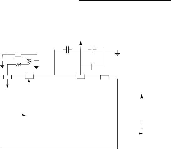
MHz. Additionally, the system clock frequency can be driven directly onto the EXTAL pin. In this case, the EXTAL frequency should be the exact system frequency desired (0 to Maximum Operating Frequency) and the XTAL pin should be left floating. Figure 2-4 shows all the external connections required for the on-chip oscillator (as well as the PLL, VCC, and GND connection
20pf 
EXTAL
VCC
~390pf x MF
CRYSTAL
330K |
20pf |
|
20M
XTAL XFC VCCSYN
0.1 F
0.01 F
GNDSYN
|
|
|
|
|
|
|
|
|
|
|
|
|
|
|
|
|
|
|
|
|
|
|
|
|
|
|
|
|
|
|
|
|
|
|
|
|
|
|
|
|
|
|
|
|
|
|
|
|
|
|
|
|
|
|
|
|
|
|
|
|
|
|
|
|
|
|
|
|
|
|
|
|
|
|
|
|
|
|
|
|
|
|
|
|
|
|
|
CRYSTAL |
|
|
|
|
|
|
|
|
VCC |
|
|||||||||||
OSCILLATOR |
|
|
|
|
|
|
|
|
|
|
|
|
|
|
|
|
|
||||
|
|
|
|
|
|
|
|
|
|
|
|
ICLVCC |
|
|
|
|
0.1 F |
||||
|
|
|
|
|
CLOCK GENERATION |
|
|
|
|
||||||||||||
|
|
|
|
|
|
|
|
||||||||||||||
|
|
|
|
|
|
|
|
|
|
|
|
|
|
|
|
|
|||||
|
|
|
|
|
|
|
|
|
|
|
|
|
|
|
|
|
|||||
|
|
|
|
|
|
|
|
ICLGND |
|
|
|
||||||||||
|
|
|
|
|
|
|
|
|
|
||||||||||||
|
|
|
|
|
|
|
|
|
|
|
|
|
|
|
|
|
|
|
|
|
|
|
|
|
|
|
|
|
|
|
|
|
|
|
|
|
|
|
|
|
|
|
|
|
|
|
|
|
|
|
|
|
|
|
|
CLKO |
|
||||||||
|
|
|
|
|
|
|
|
|
|
|
|
|
|||||||||
|
|
|
|
|
|
|
|
|
|
|
|
|
|
|
|
|
|
|
|
|
|
Figure 2-4. PLL External Components
2.4.3.3PHASE-LOCKED LOOP (PLL). The IMP PLL’s main function is frequency multiplication. The phase-locked loop takes the CLKIN frequency and outputs a high-frequency source used to derive the general system frequency of the IMP. The IMP PLL is comprised of a phase detector, loop filter, voltage-controlled oscillator (VCO), and multiplication block.
2.4.3.4FREQUENCY MULTIPLICATION. The IMP PLL can multiply the CLKIN input frequency by any integer between 1 and 4096. The multiplication factor may be changed to the desired value by writing the MF11–MF0 bits in the IPLCR. When the IMP PLL multiplier is modified in software, the IMP PLL will lose lock, and the clocking of the IMP will stop until lock is regained (worst case is 2500 EXTAL clocks). If an alteration in the system clock rate is desired without losing IMP PLL lock, the value in the low-power clock divider can be to modified to lower the system clock rate dynamically. The low power clock divider bits are located in the IOMCR register.
NOTE
If IMP PLL is enabled, the multiplication value must be large enough to result in the VCO clock being greater than 10 MHz.
MOTOROLA |
MC68LC302 REFERENCE MANUAL |
2-9 |

Configuration, Clocking, Low Power Modes, and Internal Memory Map
2.4.3.4.1 Low Power PLL Clock Divider. The output of the IMP VCO is sent to a low power divider block. The clock divider can divide the output frequency of the VCO before it generates the system clock. The clock for the baud rate generators (BRGs) bypasses this clock divider.
The purpose of the clock divider is to allow the user to reduce and restore the operating frequency of the IMP without losing the IMP’s PLL lock. Using the clock divider, the user can still obtain full IMP operation, but at a slower frequency. The BRG is not affected by the low power divider circuitry so previous BRG divider settings will not have to be changed when the divide factors are changed.
When the PLL low power divider bits (DF0–3) are programmed to a non-zero value, the IMP is in SLOW_GO mode. The selection and speed of the SLOW_GO mode may be changed at any time, with changes occurring immediately.
NOTE
The IMP low power clock divider is active only if the IMP PLL is active.
The low-power divider block is controlled in the IOMCR. The default state of the low-power divider is to divide all clocks by 1.
If the low-power divider block is not used and the user is concerned that errant software could accidentally write the IOMCR, the user may set a write protection bit in IOMCR to prevent further writes to the register.
2.4.3.4.2 IMP PLL and Clock Control Register (IPLCR). IPLCR is a 16-bit read/write register used to control the IMP’s PLL, multiplication factor and CLKO drive strength. This register is mapped in the 68000 bus space at address $0F8. If the 68000 bus is set to 8 bits (BUSW grounded at reset), during 8-bit accesses, changes to the IPLCR will take effect in the IMP PLL after loading the high byte of IPLCR (the low byte is written first). The WP bit in IPLCR is used as a protect mechanism to prevent erroneous writing. When this bit is set further accesses to the IPLCR will be blocked.
IMP PLL and Clock Control Register (IPLCR) |
|
|
|
$0F8 |
|||
15 |
14 |
13 |
12 |
11 |
10 |
9 |
8 |
|
|
|
|
|
|
|
|
IPLWP |
CLKOMOD0–1 |
PEN |
MF11 |
MF10 |
MF9 |
MF8 |
|
|
|
|
|
|
|
|
|
RESET |
|
|
|
|
|
|
|
0 |
0 |
0 |
VCCSYN |
0 |
0 |
0 |
VCCSYN/MODCLK |
7 |
6 |
5 |
4 |
|
3 |
2 |
1 |
0 |
MF7 |
MF6 |
MF5 |
MF4 |
|
MF3 |
MF2 |
MF1 |
MF0 |
|
|
|
|
|
|
|
|
|
RESET |
|
|
|
|
|
|
|
|
VCCSYN/MODCLK1 |
0 |
0 |
VCCSYN/MODCLK |
0 |
0 |
MODCLK |
MODCLK |
|
Read/Write
2-10 |
MC68LC302 REFERENCE MANUAL |
MOTOROLA |

Configuration, Clocking, Low Power Modes, and Internal Memory Map
MF 11–0—Multiplication Factor
These bits define the multiplication factor that will be applied to the IMP PLL input frequency. The multiplication factor can be any integer from 1 to 4096. The system frequency is ((MF bits + 1) x EXTAL). The multiplication factor must be chosen to ensure that the resulting VCO output frequency will be in the range from 10 MHz to the maximum allowed clock input frequency (e.g. 20 MHz for a 20 MHz IMP).
The value 000 results in a multiplier value of 1. The value $FFF results in a multiplier value of 4096.
Any time a new value is written into the MF11–MF0 bits, the IMP PLL will lose the lock condition, and after a delay of 2500 EXTAL clocks, will relock. When the IMP PLL loses its lock condition, all the clocks that are generated by the IMP PLL are disabled. After hardware reset, the MF11–MF0 bits default to either 0, 3 or 400 ($190 hex) depending on the MODCLK and VCCSYN pins (giving a multiplication factor of 1, 4 or 401). If the multiplication factor is 401, then a standard 32.768 kHz crystal generates an initial general system clock of 13.14 MHz. If the multiplication factor is 4, then a standard 4.192 MHz crystal generates an initial general system clock of 16.768 MHz. The user would then write the MF bits or adjust the output frequency to the desired frequency.
NOTE
Since the clock source for the periodic interrupt timer is CLKIN (see Figure 2-2), the PIT timer is not disturbed when the IMP PLL is in the process of acquiring lock.
PEN—PLL Enable Bit
The PEN bit indicates whether the IMP PLL is operating. This bit is written by the MC68LC302 based on the value of VCCSYN during reset. When the IMP PLL is disabled, the VCO is not operating in order to minimize power consumption. During hardware reset this bit is set if the VCCSYN pin specifies that the IMP PLL is enabled. The only way to clear PEN is to hold the VCCSYN pin low during a hardware reset.
0 = The IMP PLL is disabled. Clocks are derived directly from the EXTAL pin.
1 = The IMP PLL is enabled. Clocks are derived from the CLKOUT output of the PLL.
CLKODM0–1—CLKO Drive Mode 0–1
These bits control the output buffer strength of the CLKO pin. Those bits can be dynamically changed without generating spikes on the CLKO pin. Disabling CLKO will save power and reduce noise.
00 = Clock Out Enabled, Full-Strength Output Buffer.
01 = Clock Out Enabled, 2/3-Strength Output Buffer
10 = Clock Out Enabled, 1/3-Strength Output Buffer
11 = Clock Out Disabled (CLKO is driven high by internal pullup)
NOTE
These IMP bits are in a different address location than in the
MC68302, where they are located at address $FA (bits 15, 14).
MOTOROLA |
MC68LC302 REFERENCE MANUAL |
2-11 |

Configuration, Clocking, Low Power Modes, and Internal Memory Map
IPLWP—IMP PLL Control Write Protect Bit
This bit prevents accidental writing into the IPLCR. After reset, this bit defaults to zero to enable writing. Setting this bit prevents further writing (excluding the first write that sets this bit).
2.4.3.5 IMP INTERNAL CLOCK SIGNALS. The following paragraphs describe the IMP internal clock signals.
2.4.3.5.1IMP System Clock. The IMP system clock is supplied to all modules on the IMP (with the exception of the BRG clocks which are connected directly to the VCO output with the PLL enabled). The IMP can be programmed to operate with or without IMP PLL. If IMP PLL is active, the system clock will be driven by PLL clock divider output. If IMP PLL is not active, the system clock will be driven by the PLL input clock (CLKIN).
2.4.3.5.2BRG Clock. The clock to the BRGs can be supplied from the IMP PLL input (CLKIN) when the IMP PLL is disabled, or from the IMP PLL VCO output (when the PLL is enabled). The BRG prescaler input clock may be optionally programmed to be divided by 2 to allow very low baud rates to be generated from the system clock by setting the BCD bit in the IOMCR.
2.4.3.5.3PIT Clock. CLKIN is supplied to the periodic interrupt timer (PIT) submodule which allows the PIT clock to run independently of the system clock (refer to Figure 2-2 and Section 3 System Integration Block (SIB)).
2.4.3.6 IMP PLL PINS. The following pins are dedicated to the IMP PLL operation.
2.4.3.6.1VCCSYN. This pin is the VCC dedicated to the analog IMP PLL circuits. The voltage should be well regulated, and the pin should be provided with an extremely low-imped-
ance path to the VCC power rail if the PLL is to be enabled. VCCSYN should be bypassed to GNDSYN by a 0.1- F capacitor located as close as possible to the chip package. VCCSYN should be tied to ground if the PLL is to be disabled.
2.4.3.6.2GNDSYN. This pin is the GND dedicated to the analog IMP PLL circuits. The pin
should be provided with an extremely low-impedance path to ground. GDNSYN should be bypassed to VCCSYN by a 0.1 F capacitor located as close as possible to the chip package. The user should also bypass GNDSYN to VCCSYN with a 0.01 F capacitor as close as possible to the chip package.
2.4.3.6.3XFC. This pin connects to the off-chip capacitor for the PLL filter. One terminal of the capacitor is connected to XFC; the other terminal is connected to IQVCC.
2.4.3.6.4MODCLK. MODCLK specifies what the initial VCO frequency is after a hardware reset if VCCSYN is tied high. During the assertion of RESET, the value of the VCCSYN and MODCLK input pins causes the PEN bit and the MF11–0 bits of the IMP PLL and Clock Control Register (IPLCR) $0F8 to be appropriately written.VCCSYN and MODCLK also determines if the oscillator’s prescaler is used. After RESET is negated, the MODCLK pins is ignored and becomes PA12. Table 2-2 shows the combinations of VCCSYN and MODCLK pins with the corresponding default settings.
2-12 |
MC68LC302 REFERENCE MANUAL |
MOTOROLA |

Configuration, Clocking, Low Power Modes, and Internal Memory Map
2.4.4 IMP Power Management
The IMP portion of the MC68LC302 has several low power modes from which to choose.
2.4.4.1 IMP LOW POWER MODES. The MC68LC302 provides a number of low power modes for the IMP section. Each of the operation modes has different current consumption, wake-up time, and functionality characteristics. The state of the IMP’s 68000 data and address bus lines can be either driven high, low or high impedance during low power stop mode by programming the low power drive control register (LPDCR).
NOTE
For lowest current consumption, the SCCs and BRGs should be disabled before entering the low power modes. Current consumption for all operating modes is specified in Section 6 Electrical Characteristics.
Table 2-3. IMP Low Power Modes - IMP PLL Enabled
Operation |
|
|
|
Wake_Up |
Current |
Method of Entry/ |
IMP |
|
Oscillator |
PLL |
IMP Clock |
(Osc. Clock |
Consumption |
||||
Mode |
LPM bits |
Functionality |
||||||
|
|
|
Cycles) |
(Approximate) |
||||
|
|
|
|
|
|
|||
|
|
|
|
|
|
|
|
|
STOP |
Not Active |
Not active |
Not active |
70000 osc. |
<0.1mA |
Stop instruction/ |
No |
|
clocks |
LPM1–0=11 |
|||||||
|
|
|
|
|
|
|||
DOZE |
Active |
Not active |
Not active |
2500 osc |
About 500uA |
Stop instruction/ |
No |
|
clocks |
LPM1–0=10 |
|||||||
|
|
|
|
|
|
|||
STAND_BY |
Active |
Active (if |
Not active |
2–5 system |
About 5mA |
Stop instruction/ |
Partial (BRG |
|
enabled |
clock cycles |
LPM1–0=01 |
clock is active) |
|||||
|
|
|
|
|||||
SLOW_GO/ |
Active |
Active (if |
Active |
|
Low, depends on |
Write to DF3–0 |
Full |
|
NORMAL |
|
enabled) |
|
|
CLK freq. |
|
|
2.4.4.1.1 STOP Mode. In STOP mode, all parts of IMP are inactive and the current consumption is less than 0.1mA. Both the crystal oscillator and the IMP PLL are shut down. Because both the oscillator and the PLL must start up, the wake-up time takes 70000 EXTAL clocks (for example, 70000 cycles of 32.768 kHz crystal will take about 2.2 seconds).
The STOP mode is entered by executing the STOP instruction with the LPM0–1 bits in the IOMCR register set to 11. Refer to 2.4.4.2.2 Entering the STOP/ DOZE/ STAND_BY Mode for an example instruction sequence for use with the STOP instruction.
2.4.4.1.2 DOZE Mode. In DOZE mode, the oscillator is active in the IMP but the IMP PLL is shut down. The current consumption depends on the frequency of the external crystal but is on the order of 500 A. In DOZE mode, the IMP is shut down. The wake-up time is 2500 cycles of the external crystal (for example, 2500 cycles of 32.768 kHz crystal will take about 80 milliseconds.). Doze mode has faster wake-up time than the STOP mode, at the price of higher current consumption.
The DOZE mode is entered by executing the STOP instruction with the LPM1–0 bits in the IOMCR register set to 10. Refer to 2.4.4.2.2 Entering the STOP/ DOZE/ STAND_BY Mode for an example instruction sequence for use with the STOP instruction.
2.4.4.1.3 STAND_BY Mode. In STAND_BY mode, the oscillator is active, and the IMP PLL, if enabled, is active but the IMP clock is not active and the IMP is shut down. Current con-
MOTOROLA |
MC68LC302 REFERENCE MANUAL |
2-13 |

Configuration, Clocking, Low Power Modes, and Internal Memory Map
sumption in STAND-BY mode is less than less than 5mA. The wake up time is a few IMP system clock cycles.
The STAND_BY mode is entered by executing the STOP instruction with the LPM1–0 bits in the IOMCR register set to 01. Refer to 2.4.4.2.2 Entering the STOP/ DOZE/ STAND_BY Mode for an example instruction sequence for use with the STOP instruction.
2.4.4.1.4SLOW_GO Mode. In the SLOW-GO mode, the IMP is fully operational but the IMP PLL divider has been programmed with a value that is dividing the IMP PLL VCO output to the system clock in order to save power. The PLL output divider can only be used with
the IMP PLL enabled. The divider value is programmed in the DF3–0 bits in the IOMCR. The clock may be divided by a power of 2 (20 – 215). No functionality is lost in SLOW-GO mode.
2.4.4.1.5NORMAL Mode. In NORMAL mode the IMP part is fully operational and the system clock from the PLL is not being divided down.
2.4.4.1.6IMP Operation Mode Control Register (IOMCR). IOMCR is a 8-bit read/ write register used to control the operation modes of the IMP. The WP bit in IOMCR is used as a protect mechanism to prevent erroneous writing of IOMCR.
IOMCR |
|
|
|
|
|
|
$0FA |
|
7 |
6 |
5 |
4 |
3 |
2 |
1 |
0 |
|
|
|
|
|
|
|
|
|
|
IOMWP |
DF3 |
DF2 |
DF1 |
DF0 |
BCD |
LPM1 |
LPM0 |
|
|
|
|
|
|
|
|
|
|
RESET: |
0 |
0 |
0 |
0 |
0 |
0 |
0 |
|
0 |
||||||||
|
|
|
|
|
|
|
Read/Write
IOMWP—IMP Operation Mode Control Write Protect Bit
This bit prevents accidental writing into the IOMCR. After reset, this bit defaults to zero to enable writing. Setting this bit prevents further writing (excluding the first write that sets this bit).
DF 3–0—Divide Factor
The Divide Factor Bits define the divide factor of the low power divider of the PLL. These bits specify a divide range between 20 and 215. Changing the value of these bits will not cause a loss of lock condition to the IMP PLL.
BCD—BRG Clock Divide Control
This bit controls whether the divide-by-two block shown in Figure 2-2 is enabled.
0 = The BRG clock is divided by 1.
1 = The BRG clock is divided by 2.
2-14 |
MC68LC302 REFERENCE MANUAL |
MOTOROLA |

Configuration, Clocking, Low Power Modes, and Internal Memory Map
LPM—Low Power Modes
When the 68000 core executes the STOP instruction, the IMP will enter the specified mode.
LPM1–0:
00 = Normal - the IMP PLL and clock oscillator will continue to operate normally. 01 = Stand_by Mode
10 = DOZE Mode
11 = Stop Mode
2.4.4.1.7 Low Power Drive Control Register (LPDCR). This register controls the state of the IMP’s 68000 address and data buses during the Standby, Doze, and Stop modes. By programming this register it is possible to minimize power consumption due to external pullups or pull downs, or floating inputs.
LPDCR |
|
|
|
|
|
|
BAR+$82A |
|
7 |
6 |
5 |
4 |
3 |
2 |
1 |
0 |
|
|
|
|
|
|
|
|
|
|
|
|
|
|
|
LPAL |
LPDL |
LPDEN |
|
|
|
|
|
|
|
|
|
|
RESET: |
0 |
0 |
0 |
0 |
0 |
0 |
0 |
|
0 |
||||||||
|
|
|
|
|
|
|
Read/Write
LPDEN—Low Power Drive Enable
0 - The IMP 68000 data and address buses will be high impedance.
1 - The IMP 68000 data and address buses to be driven according to the LPDL bit.
LPDL—Low Power Drive Data Low
0 - The data bus will be driven high when the LPDEN bit is set. 1 - The data bus will be driven low when the LPDEN bit is set.
LPAL-Low Power Drive Address Low
0 - The address bus will be driven high when the LPDEN bit is set. 1 - The address bus will be driven low when the LPDEN bit is set.
2.4.4.1.8IMP Power Down Register (IPWRD). The IPWRD is a 8-bit read/ write register located at $0FB that is used to control the low power operation of the IMP. This register must be written with the same operand as the STOP instruction that follows. This tells the hardware what level of interrupt (and above) will stop the MC68LC302 from entering low power if it occurs while the clocks are being stopped.
2.4.4.1.9Default Operation Modes, See 2.4.2.1 Default System Clock Generation.
2.4.4.2 LOW POWER SUPPORT. The following sections describe how to enter the various low power modes.
2.4.4.2.1 Enter the SLOW_GO mode. When the required IMP performance can be achieved with a lower clock rate, the user can reduce power consumption by dividing IMP
MOTOROLA |
MC68LC302 REFERENCE MANUAL |
2-15 |

Configuration, Clocking, Low Power Modes, and Internal Memory Map
PLL output clock that provides the IMP system clock. Switching between the NORMAL and SLOW_GO modes is achieved by changing the DF3–0 field in the IOMCR register to a nonzero value. The IMP PLL will not lose lock when the DF3–0 field in the IOMCR register is changed.
2.4.4.2.2 Entering the STOP/ DOZE/ STAND_BY Mode. Entering the STOP/ DOZE/ STAND_BY mode is achieved by the 68000 core executing the following code:
nop |
|
|
move.b |
*+6(PC),$000000FB |
;copy STOP operand high byte to addr 000000fb |
stop |
#$xxxx |
;xxxx -> SR |
nop |
|
|
This code is position independent. The core must be in the supervisor state to execute the STOP instruction, therefore the write to $000000FB must be done in the supervisor state (function code 5, supervisor data). The core trace exception should be disabled, otherwise the low power control will not enter the STOP mode.
To guarantee supervisor state and trace exceptions disabled, this code should be part of a TRAP routine. Upon entering the trap routine, examine the stacked status register. If it indicates the supervisor state, then execute this code to enter STOP mode. If not supervisor, do NOT execute this code (could perform some application-specific error):
TRAP_x |
btst.b |
#5,(SP) |
; supervisor? |
|
beq.s |
NO_STOP |
|
|
nop |
|
; flush execution, bus pipes |
|
move.b |
*+6(PC),$000000FB |
;copy STOP operand high byte to addr 000000fb |
|
stop |
#$xxxx |
; xxxx -> SR |
|
nop |
|
|
|
rte |
|
|
NO_STOP |
... |
|
; error routine? |
NOTE
The RI/PB9, DTE/PB10, and periodic interrupt timer timeout interrupts conditions will generate level 4 interrupts. The user should set the 68000 interrupt mask register to the appropriate level before executing this code.
IMP’s low power control logic will:
1.Detect the write cycle.
2.Check if bit 5 = 1 (supervisor space) (if it is 0, the low power request will be ignored).
3.Sample the interrupt mask bits (bits 0–2). If during this process of stopping the clocks
2-16 |
MC68LC302 REFERENCE MANUAL |
MOTOROLA |

Configuration, Clocking, Low Power Modes, and Internal Memory Map
an interrupt of higher level than the mask is asserted to the core, this process will abort.
4.Wait for 16 clocks to guarantee the execution of the STOP command by the core. BG and BGACK will reset the 16-clock counter and it will restart its count.
5.Assert bus request signal to the core.
6.Wait for Bus Grant from the core
7.Force the IMP to the selected power-down mode, as defined in Table 2-3.
2.4.4.2.3 IMP Wake-Up from Low Power STOP Modes. The IMP can wake up from STOP/DOZE/STAND_BY mode to NORMAL/SLOW_GO mode in response to inputs from the following sources:
1.Asserting both RESET and HALT (hard reset) pins.
2.Asserting (high to low transition) either PB9 or PB10 pins (if these interrupts are enabled).
3.A timeout of the periodic interrupt timer (if the PIT interrupt is enabled).
When one of these events occur (and the corresponding event bit is set), the IMP low power controller will asynchronously restart the IMP clocks. Then IMP low power control logic will release the 68000 bus and the IMP will return to normal operation. If one of the above wakeup events occurs during the execution of the STOP command, the low power control logic will abort the power down sequence and return to normal operation.
NOTE
The RI/PB9, DTE/PB10, and periodic interrupt timer timeout interrupts conditions will generate level 4 interrupts.The user should also set the 68000 interrupt mask in the status register (SR) to the appropriate level before executing the STOP command to ensure that the IMP will wake up to the desired events.
2.4.4.2.4 IMP Wake-Up Control Register (IWUCR). The IWUCR contains control for the wake-up options. This register can be read and written by the 68000 core.
IWUCR |
|
|
|
|
|
|
$0F7 |
||
7 |
6 |
5 |
4 |
3 |
2 |
1 |
0 |
||
|
|
|
|
|
|
|
|
||
|
0 |
PITE |
PB10E |
PB9Ev |
0 |
PITEn |
PB10En |
PB9En |
|
|
|
|
|
|
|
|
|
|
|
|
RESET: |
0 |
0 |
0 |
0 |
0 |
0 |
0 |
|
0 |
|||||||||
|
|
|
|
|
|
|
|||
Read/Write
PB9Ev—PB9 Event
This bit will be set to one when there is a high to low transition on the PB9 pin. When PB9En is set and PB9Ev is set, the IMP will wake-up from the selected power down state, and a PB9 Interrupt will be generated. The IMP cannot enter the power-down mode if
MOTOROLA |
MC68LC302 REFERENCE MANUAL |
2-17 |
 Loading...