


 Loading...
Motorola MC68L11K0FN1, MC68L11K3FN1, MC68L11K3FU1, MC68L11K3FU3, MC68L11K4FN3 Datasheet
...MOTOROLA
SEMICONDUCTOR
TECHNICAL DATA
Order this document by MC68HC11KTS/D
M68HC11 K Series
Technical Summary
8-Bit Microcontroller
The M68HC11 K-series microcontroller units (MCUs) are high-performance derivatives of the MC68HC11F1 and have several additional features. The MC68HC11K0, MC68HC11K1, MC68HC11K3, MC68HC11K4 and MC68HC711K4 comprise the series. These MCUs, with a nonmultiplexed expanded bus, are characterized by high speed and low power consumption. Their fully static design allows operation at frequencies from 4 MHz to dc.
This document contains information concerning standard, custom-ROM, and extended-voltage devices. Standard devices include those with disabled ROM (MC68HC11K1), disabled EEPROM (MC68HC11K3), disabled ROM and EEPROM (MC68HC11K0), or EPROM replacing ROM (MC68HC711K4). Custom-ROM devices have a ROM array that is programmed at the factory to customer specifications. Extended-voltage devices are guaranteed to operate over a much greater voltage range (3.0 Vdc to 5.5 Vdc) at lower frequencies than the standard devices. Refer to the device ordering information tables for details concerning these differences.
1Features
•M68HC11 CPU
•Power Saving STOP and WAIT Modes
•768 Bytes RAM (All Saved During Standby)
•24 Kbytes ROM or EPROM
•640 Bytes Electrically Erasable Programmable Read Only Memory (EEPROM)
•Optional Security Feature Protects Memory Contents
•On-Chip Memory Mapping Logic Allows Expansion to Over 1 Mbyte of Address Space
•PROG Mode Allows Use of Standard EPROM Programmer (27C256 Footprint)
•Nonmultiplexed Address and Data Buses
•Four Programmable Chip Selects with Clock Stretching (Expanded Modes)
•Enhanced 16-Bit Timer with Four-Stage Programmable Prescaler
—Three Input Capture (IC) Channels
—Four Output Compare (OC) Channels
—One Additional Channel, Selectable as Fourth IC or Fifth OC
•8-Bit Pulse Accumulator
•Four 8-Bit or Two 16-Bit Pulse Width Modulation (PWM) Timer Channels
•Real-Time Interrupt Circuit
•Computer Operating Properly (COP) Watchdog
•Clock Monitor
•Enhanced Asynchronous Nonreturn to Zero (NRZ) Serial Communications Interface (SCI)
•Enhanced Synchronous Serial Peripheral Interface (SPI)
•Eight-Channel 8-Bit Analog-to-Digital (A/D) Converter
•Seven Bidirectional Input/Output (I/O) Ports (54 Pins)
•One Fixed Input-Only Port (8 Pins)
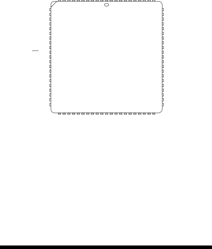
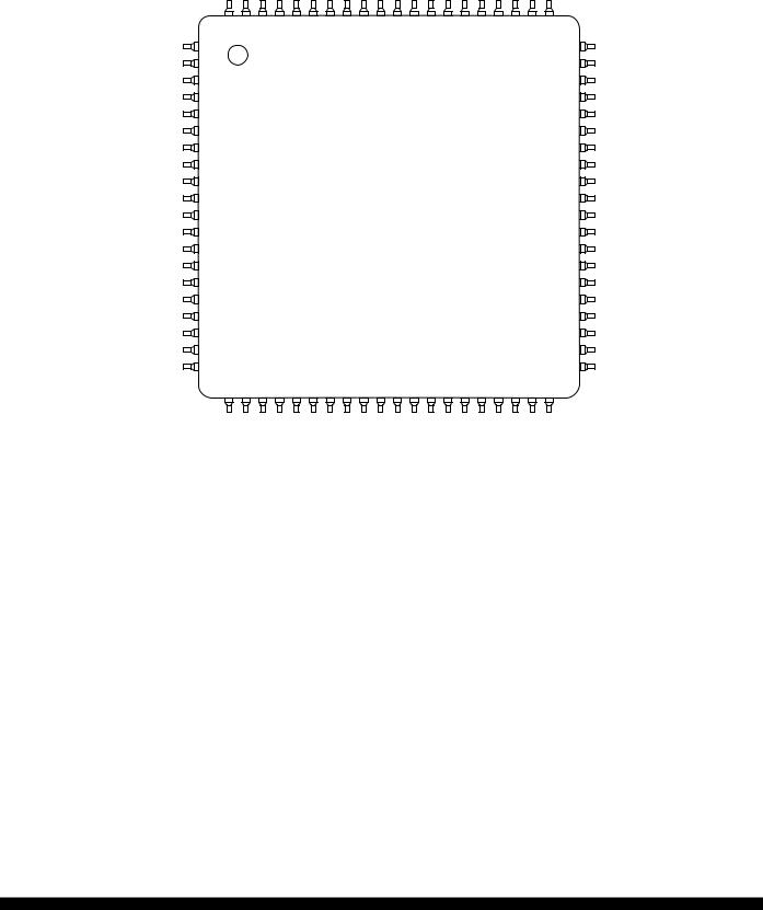
•Available in 84-Pin Plastic Leaded Chip Carrier (PLCC), 84-Pin Windowed Ceramic Leaded Chip Carrier (CLCC), and 80-Pin Quad Flat Pack (QFP)
This document contains information on a new product. Specifications and information herein are subject to change without notice.
© MOTOROLA INC., 1997

Table 1 Standard Device Ordering Information
Package |
Temperature |
CONFIG |
Description |
Frequency |
MC Order Number |
|
|
|
|
|
|
84-Pin PLCC |
–40°to + 85°C |
$DF |
BUFFALO ROM |
4 MHz |
MC68HC11K4BCFN4 |
|
|
|
|
|
|
|
–40°to + 85°C |
$DD |
No ROM |
2 MHz |
MC68HC11K1CFN2 |
|
|
|
|
|
|
|
|
|
|
3 MHz |
MC68HC11K1CFN3 |
|
|
|
|
|
|
|
|
|
|
4 MHz |
MC68HC11K1CFN4 |
|
|
|
|
|
|
|
–40°to + 105°C |
$DD |
No ROM |
2 MHz |
MC68HC11K1VFN2 |
|
|
|
|
|
|
|
|
|
|
3 MHz |
MC68HC11K1VFN3 |
|
|
|
|
|
|
|
|
|
|
4 MHz |
MC68HC11K1VFN4 |
|
|
|
|
|
|
|
–40°to + 125°C |
$DD |
No ROM |
2 MHz |
MC68HC11K1MFN2 |
|
|
|
|
|
|
|
|
|
|
3 MHz |
MC68HC11K1MFN3 |
|
|
|
|
|
|
|
|
|
|
4 MHz |
MC68HC11K1MFN4 |
|
|
|
|
|
|
|
–40°to + 85°C |
$DC |
No ROM, No EEPROM |
2 MHz |
MC68HC11K0CFN2 |
|
|
|
|
|
|
|
|
|
|
3 MHz |
MC68HC11K0CFN3 |
|
|
|
|
|
|
|
|
|
|
4 MHz |
MC68HC11K0CFN4 |
|
|
|
|
|
|
|
–40°to + 105°C |
$DC |
No ROM, No EEPROM |
2 MHz |
MC68HC11K0VFN2 |
|
|
|
|
|
|
|
|
|
|
3 MHz |
MC68HC11K0VFN3 |
|
|
|
|
|
|
|
|
|
|
4 MHz |
MC68HC11K0VFN4 |
|
|
|
|
|
|
|
–40°to + 125°C |
$DC |
No ROM, No EEPROM |
2 MHz |
MC68HC11K0MFN2 |
|
|
|
|
|
|
|
|
|
|
3 MHz |
MC68HC11K0MFN3 |
|
|
|
|
|
|
|
|
|
|
4 MHz |
MC68HC11K0MFN4 |
|
|
|
|
|
|
|
–40°to + 85°C |
$DF |
OTPROM |
2 MHz |
MC68HC711K4CFN2 |
|
|
|
|
|
|
|
|
|
|
3 MHz |
MC68HC711K4CFN3 |
|
|
|
|
|
|
|
|
|
|
4 MHz |
MC68HC711K4CFN4 |
|
|
|
|
|
|
|
–40°to + 105°C |
$DF |
OTPROM |
2 MHz |
MC68HC711K4VFN2 |
|
|
|
|
|
|
|
|
|
|
3 MHz |
MC68HC711K4VFN3 |
|
|
|
|
|
|
|
|
|
|
4 MHz |
MC68HC711K4VFN4 |
|
|
|
|
|
|
|
–40°to + 125°C |
$DF |
OTPROM |
2 MHz |
MC68HC711K4MFN2 |
|
|
|
|
|
|
|
|
|
|
3 MHz |
MC68HC711K4MFN3 |
|
|
|
|
|
|
|
|
|
|
4 MHz |
MC68HC711K4MFN4 |
|
|
|
|
|
|
80-Pin QFP |
–40°to + 85°C |
$DF |
BUFFALO ROM |
4 MHz |
MC68HC11K4BCFU4 |
(14 mm X 14 |
|
|
|
|
|
–40°to + 85°C |
$DD |
No ROM |
2 MHz |
MC68HC11K1CFU2 |
|
mm) |
|
|
|
|
|
|
|
|
3 MHz |
MC68HC11K1CFU3 |
|
|
|
|
|
||
|
|
|
|
|
|
|
|
|
|
4 MHz |
MC68HC11K1CFU4 |
|
|
|
|
|
|
|
–40°to + 105°C |
$DD |
No ROM |
2 MHz |
MC68HC11K1VFU2 |
|
|
|
|
|
|
|
|
|
|
3 MHz |
MC68HC11K1VFU3 |
|
|
|
|
|
|
|
|
|
|
4 MHz |
MC68HC11K1VFU4 |
|
|
|
|
|
|
|
–40°to + 85°C |
$DC |
No ROM, No EEPROM |
2 MHz |
MC68HC11K0CFU2 |
|
|
|
|
|
|
|
|
|
|
3 MHz |
MC68HC11K0CFU3 |
|
|
|
|
|
|
|
|
|
|
4 MHz |
MC68HC11K0CFU4 |
|
|
|
|
|
|
|
–40°to + 105°C |
$DC |
No ROM, No EEPROM |
2 MHz |
MC68HC11K0VFU2 |
|
|
|
|
|
|
|
|
|
|
3 MHz |
MC68HC11K0VFU3 |
|
|
|
|
|
|
|
|
|
|
4 MHz |
MC68HC11K0VFU4 |
|
|
|
|
|
|
MOTOROLA |
M68HC11 K Series |
2 |
MC68HC11KTS/D |

Table 1 Standard Device Ordering Information (Continued)
Package |
Temperature |
CONFIG |
Description |
Frequency |
MC Order Number |
|
|
|
|
|
|
84-Pin CLCC |
–40°to + 85°C |
$DF |
EPROM |
2 MHz |
MC68HC711K4CFS2 |
(Windowed) |
|
|
|
|
|
|
|
|
3 MHz |
MC68HC711K4CFS3 |
|
|
|
|
|
||
|
|
|
|
|
|
|
|
|
|
4 MHz |
MC68HC711K4CFS4 |
|
|
|
|
|
|
|
–40°to + 105°C |
$DF |
EPROM |
2 MHz |
MC68HC711K4VFS2 |
|
|
|
|
|
|
|
|
|
|
3 MHz |
MC68HC711K4VFS3 |
|
|
|
|
|
|
|
|
|
|
4 MHz |
MC68HC711K4VFS4 |
|
|
|
|
|
|
|
–40°to + 125°C |
$DF |
EPROM |
2 MHz |
MC68HC711K4MFS2 |
|
|
|
|
|
|
|
|
|
|
3 MHz |
MC68HC711K4MFS3 |
|
|
|
|
|
|
|
|
|
|
4 MHz |
MC68HC711K4MFS4 |
|
|
|
|
|
|
Table 2 Extended Voltage (3.0 Vdc to 5.5 Vdc) Device Ordering Information
Package |
Temperature |
Description |
Frequency |
MC Order Number |
|
|
|
|
|
84-Pin PLCC |
–20°to + 70°C |
Custom ROM |
1 MHz |
MC68L11K4FN1 |
|
|
|
|
|
|
|
|
3 MHz |
MC68L11K4FN3 |
|
|
|
|
|
|
|
No ROM |
1 MHz |
MC68L11K1FN1 |
|
|
|
|
|
|
|
|
3 MHz |
MC68L11K1FN3 |
|
|
|
|
|
|
|
No ROM, No EEPROM |
1 MHz |
MC68L11K0FN1 |
|
|
|
|
|
|
|
|
3 MHz |
MC68L11K0FN3 |
|
|
|
|
|
|
|
Custom ROM, No EEPROM |
1 MHz |
MC68L11K3FN1 |
|
|
|
|
|
|
|
|
3 MHz |
MC68L11K3FN3 |
|
|
|
|
|
80-Pin QFP |
–20°to + 70°C |
Custom ROM |
1 MHz |
MC68L11K4FU1 |
|
|
|
|
|
|
|
|
3 MHz |
MC68L11K4FU3 |
|
|
|
|
|
|
|
No ROM |
1 MHz |
MC68L11K1FU1 |
|
|
|
|
|
|
|
|
3 MHz |
MC68L11K1FU3 |
|
|
|
|
|
|
|
No ROM, No EEPROM |
1 MHz |
MC68L11K0FU1 |
|
|
|
|
|
|
|
|
3 MHz |
MC68L11K0FU3 |
|
|
|
|
|
|
|
Custom ROM, No EEPROM |
1 MHz |
MC68L11K3FU1 |
|
|
|
|
|
|
|
|
3 MHz |
MC68L11K3FU3 |
|
|
|
|
|
M68HC11 K Series |
MOTOROLA |
MC68HC11KTS/D |
3 |

Table 3 Custom ROM Device Ordering Information
Package |
Temperature |
Description |
Frequency |
MC Order Number |
|
|
|
|
|
84-Pin PLCC |
–40°to + 85°C |
Custom ROM |
2 MHz |
MC68HC11K4CFN2 |
|
|
|
|
|
|
|
|
3 MHz |
MC68HC11K4CFN3 |
|
|
|
|
|
|
|
|
4 MHz |
MC68HC11K4CFN4 |
|
|
|
|
|
|
–40°to + 105°C |
Custom ROM |
2 MHz |
MC68HC11K4VFN2 |
|
|
|
|
|
|
|
|
3 MHz |
MC68HC11K4VFN3 |
|
|
|
|
|
|
|
|
4 MHz |
MC68HC11K4VFN4 |
|
|
|
|
|
|
–40°to + 125°C |
Custom ROM |
2 MHz |
MC68HC11K4MFN2 |
|
|
|
|
|
|
|
|
3 MHz |
MC68HC11K4MFN3 |
|
|
|
|
|
|
|
|
4 MHz |
MC68HC11K4MFN4 |
|
|
|
|
|
|
–40°to + 85°C |
Custom ROM, No EEPROM |
2 MHz |
MC68HC11K3CFN2 |
|
|
|
|
|
|
|
|
3 MHz |
MC68HC11K3CFN3 |
|
|
|
|
|
|
|
|
4 MHz |
MC68HC11K3CFN4 |
|
|
|
|
|
|
–40°to + 105°C |
Custom ROM, No EEPROM |
2 MHz |
MC68HC11K3VFN2 |
|
|
|
|
|
|
|
|
3 MHz |
MC68HC11K3VFN3 |
|
|
|
|
|
|
|
|
4 MHz |
MC68HC11K3VFN4 |
|
|
|
|
|
|
–40°to + 125°C |
Custom ROM, No EEPROM |
2 MHz |
MC68HC11K3MFN2 |
|
|
|
|
|
|
|
|
3 MHz |
MC68HC11K3MFN3 |
|
|
|
|
|
|
|
|
4 MHz |
MC68HC11K3MFN4 |
|
|
|
|
|
80-Pin QFP |
–40°to + 85°C |
Custom ROM |
2 MHz |
MC68HC11K4CFU2 |
|
|
|
|
|
|
|
|
3 MHz |
MC68HC11K4CFU3 |
|
|
|
|
|
|
|
|
4 MHz |
MC68HC11K4CFU4 |
|
|
|
|
|
|
–40°to + 105°C |
Custom ROM |
2 MHz |
MC68HC11K4VFU2 |
|
|
|
|
|
|
|
|
3 MHz |
MC68HC11K4VFU3 |
|
|
|
|
|
|
|
|
4 MHz |
MC68HC11K4VFU4 |
|
|
|
|
|
|
–40°to + 85°C |
Custom ROM, No EEPROM |
2 MHz |
MC68HC11K3CFU2 |
|
|
|
|
|
|
|
|
3 MHz |
MC68HC11K3CFU3 |
|
|
|
|
|
|
|
|
4 MHz |
MC68HC11K3CFU4 |
|
|
|
|
|
|
–40°to + 105°C |
Custom ROM, No EEPROM |
2 MHz |
MC68HC11K3VFU2 |
|
|
|
|
|
|
|
|
3 MHz |
MC68HC11K3VFU3 |
|
|
|
|
|
|
|
|
4 MHz |
MC68HC11K3VFU4 |
|
|
|
|
|
MOTOROLA |
M68HC11 K Series |
4 |
MC68HC11KTS/D |
|
|
|
|
|
|
|
|
PB0/ADDR8 |
PB1/ADDR9 |
PB2/ADDR10 |
PB3/ADDR11 |
PB4/ADDR12 |
PB5/ADDR13 |
PB6/ADDR14 |
PB7/ADDR15 |
V |
V |
PA0/IC3 |
PA1/IC2 |
PA2/IC1 |
PA3/OC5/IC4/OC1 |
PA4/OC4/OC1 |
PA5/OC3/OC1 |
PA6/OC2/OC1 |
PA7/PAI/OC1 |
|
PD5/SS |
PD4/SCK |
PD3/MOSI |
|
|
|
|
|
|
|
|
|
|
|
|
|
|
|
|
|
|
|
|||||||||||||||||||||||
|
|
|
|
|
|
|
|
|
|
|
|
|
|
|
|
SS |
DD |
|
|
|
|
|
|
|
|
|
|
|
|
|
|
|
|
|
|
|
|
|
|
|
|
|
|
10 |
9 |
8 |
7 |
6 |
5 |
4 |
3 |
2 |
|
84 |
83 |
82 |
81 |
80 |
79 |
78 |
77 |
76 |
75 |
|
|
|
|
|
|
||
|
|
|
|
|
|
|
|
11 |
|
|
|
|
|
|
|
||||||||||||||||||||
|
|
|
|
|
|
|
|
|
|
|
|
|
|
|
|
|
|
|
|
|
|
|
|
|
|
|
|
PD2/MISO |
|||||||
|
|
PH0/PW1 |
|
|
|
|
|
|
|
|
|
|
|
|
1 |
|
|
|
|
|
|
|
|
|
|
74 |
|
||||||||
|
|
12 |
|
|
|
|
|
|
|
|
|
|
|
|
|
|
|
|
|
|
|
|
|
||||||||||||
|
|
PH1/PW2 |
13 |
|
|
|
|
|
|
|
|
|
|
|
|
|
|
|
|
|
|
|
|
|
73 |
|
PD1/TxD |
||||||||
|
PH2/PW3 |
14 |
|
|
|
|
|
|
|
|
|
|
|
|
|
|
|
|
|
|
|
|
|
72 |
|
PD0/RxD |
|||||||||
|
PH3/PW4 |
15 |
|
|
|
|
|
|
|
|
|
|
|
|
|
|
|
|
|
|
|
|
|
71 |
|
|
|
|
|
|
|||||
|
|
|
|
|
|
|
|
|
|
|
|
|
|
|
|
|
|
|
|
|
|
MODA/LIR |
|
||||||||||||
|
PH4/CSIO |
16 |
|
|
|
|
|
|
|
|
|
|
|
|
|
|
|
|
|
|
|
|
|
70 |
|
MODB/VSTBY |
|||||||||
|
PH5/CSGP1 |
17 |
|
|
|
|
|
|
|
|
|
|
|
|
|
|
|
|
|
|
|
|
|
69 |
|
RESET |
|
||||||||
|
PH6/CSGP2 |
18 |
|
|
|
|
|
|
|
|
|
|
|
|
|
|
|
|
|
|
|
|
|
68 |
|
XTAL |
|||||||||
|
|
|
|
19 |
|
|
|
|
|
|
|
|
|
|
|
|
|
|
|
|
|
|
|
|
|
67 |
EXTAL |
||||||||
PH7/CSPROG |
|
|
|
|
|
|
|
|
|
|
|
|
|
|
|
|
|
|
|
|
|||||||||||||||
|
|
TEST161 |
20 |
|
|
|
|
|
|
|
|
|
|
|
|
|
|
|
|
|
|
|
|
|
66 |
|
XOUT |
||||||||
|
XIRQ/VPPE2 |
21 |
|
|
|
|
|
|
|
|
|
|
|
|
|
|
|
|
|
|
|
|
|
65 |
|
E |
|||||||||
|
|
TEST151 |
22 |
|
|
|
|
|
|
|
MC68HC11K SERIES |
|
|
|
|
|
|
|
64 |
|
VDD |
||||||||||||||
|
|
VDD |
23 |
|
|
|
|
|
|
|
|
|
|
|
|
|
|
|
|
|
|
|
|
|
63 |
|
VSS |
||||||||
|
|
VSS |
24 |
|
|
|
|
|
|
|
|
|
|
|
|
|
|
|
|
|
|
|
|
|
62 |
|
PC7/DATA7 |
||||||||
|
|
TEST141 |
25 |
|
|
|
|
|
|
|
|
|
|
|
|
|
|
|
|
|
|
|
|
|
61 |
|
PC6/DATA6 |
||||||||
|
|
PG7/R/W |
|
|
|
26 |
|
|
|
|
|
|
|
|
|
|
|
|
|
|
|
|
|
|
|
|
|
60 |
|
PC5/DATA5 |
|||||
|
|
|
|
|
|
|
|
|
|
|
|
|
|
|
|
|
|
|
|
|
|
||||||||||||||
|
|
PG6 |
27 |
|
|
|
|
|
|
|
|
|
|
|
|
|
|
|
|
|
|
|
|
|
59 |
|
PC4/DATA4 |
||||||||
|
PG5/XA18 |
28 |
|
|
|
|
|
|
|
|
|
|
|
|
|
|
|
|
|
|
|
|
|
58 |
|
PC3/DATA3 |
|||||||||
|
PG4/XA17 |
29 |
|
|
|
|
|
|
|
|
|
|
|
|
|
|
|
|
|
|
|
|
|
57 |
|
PC2/DATA2 |
|||||||||
|
PG3/XA16 |
30 |
|
|
|
|
|
|
|
|
|
|
|
|
|
|
|
|
|
|
|
|
|
56 |
|
PC1/DATA1 |
|||||||||
|
PG2/XA15 |
31 |
|
|
|
|
|
|
|
|
|
|
|
|
|
|
|
|
|
|
|
|
|
55 |
|
PC0/DATA0 |
|||||||||
|
PG1/XA14 |
32 |
|
|
|
|
|
|
|
|
|
|
|
|
|
|
|
|
|
|
|
|
|
54 |
|
|
|
||||||||
|
|
|
|
|
|
|
|
|
|
|
|
|
|
|
|
|
|
|
|
|
|
IRQ |
|||||||||||||
|
|
|
|
|
|
33 |
34 |
35 |
36 |
37 |
38 |
39 |
40 |
41 |
42 |
43 |
44 |
45 |
46 |
47 |
48 |
49 |
50 |
51 |
52 |
53 |
|
|
|
|
|
|
|||
|
|
|
|
|
|
|
|
PG0/XA13 |
AV |
PE7/AN7 |
PE6/AN6 |
PE5/AN5 |
PE4/AN4 |
PE3/AN3 |
PE2/AN2 |
PE1/AN1 |
PE0/AN0 |
V |
V |
AV |
PF7/ADDR7 |
PF6/ADDR6 |
PF5/ADDR5 |
PF4/ADDR4 |
PF3/ADDR3 |
|
PF2/ADDR2 |
PF1/ADDR1 |
PF0/ADDR0 |
|
|
|
|
|
|
|
|
|
|
|
|
|
|
|
DD |
|
|
|
|
|
|
|
|
RL |
RH |
SS |
|
|
|
|
|
|
|
|
|
|
|
|
|
|
|
1.Pins 20, 22, and 25 are used only during factory testing and should not be connected to external circuitry.
2.VPPE applies only to devices with EPROM.
Figure 1 Pin Assignments for 84-Pin PLCC/CLCC
M68HC11 K Series |
MOTOROLA |
MC68HC11KTS/D |
5 |
|
|
|
D2/MISOP |
PD1/TxD |
PD0/RxD |
|
MODA/LIR |
STBY |
|
|
|
|
|
|
|
|
C7/DATA7P |
C6/DATA6P |
PC5/DATA5 |
C4/DATA4P |
C3/DATA3P |
C2/DATA2P |
C1/DATA1P |
PC0/DATA0 |
|
|
|
|
|
|
|
|
|
|
|
|
|
|
|
|
|||||||||||||
|
|
|
|
MODB/V |
|
RESET |
XTAL |
EXTAL |
E |
V |
V |
IRQ |
|
|||||||||||||
|
|
|
|
|
|
|||||||||||||||||||||
|
|
|
80 |
79 |
78 |
77 |
76 |
|
|
|
73 |
|
|
DD |
SS |
69 |
|
|
66 |
65 |
64 |
63 |
62 |
|
|
|
|
|
|
|
|
|
|
|
|
|
|
|
|||||||||||||||
|
|
|
|
|
|
|
|
|
|
|
|
|
|
|||||||||||||
|
|
|
75 |
74 |
72 |
71 |
70 |
68 |
67 |
61 |
|
|||||||||||||||
PD3/MOSI |
1 |
|
|
|
|
|
|
|
|
|
|
|
|
|
|
|
|
|
|
|
|
|
60 |
PF0/ADDR0 |
||
PD4/SCK |
2 |
|
|
|
|
|
|
|
|
|
|
|
|
|
|
|
|
|
|
|
|
|
59 |
PF1/ADDR1 |
||
|
|
|
3 |
|
|
|
|
|
|
|
|
|
|
|
|
|
|
|
|
|
|
|
|
|
58 |
PF2/ADDR2 |
PD5/SS |
|
|
|
|
|
|
|
|
|
|
|
|
|
|
|
|
|
|
|
|
|
|
||||
PA7/PAI/OC1 |
4 |
|
|
|
|
|
|
|
|
|
|
|
|
|
|
|
|
|
|
|
|
|
57 |
PF3/ADDR3 |
||
PA6/OC2/OC1 |
5 |
|
|
|
|
|
|
|
|
|
|
|
|
|
|
|
|
|
|
|
|
|
56 |
PF4/ADDR4 |
||
PA5/OC3/OC1 |
6 |
|
|
|
|
|
|
|
|
|
|
|
|
|
|
|
|
|
|
|
|
|
55 |
PF5/ADDR5 |
||
PA4/OC4/OC1 |
7 |
|
|
|
|
|
|
|
|
|
|
|
|
|
|
|
|
|
|
|
|
|
54 |
PF6/ADDR6 |
||
PA3/OC5/IC4/OC1 |
8 |
|
|
|
|
|
|
|
|
|
|
|
|
|
|
|
|
|
|
|
|
|
53 |
PF7/ADDR7 |
||
PA2/IC1 |
9 |
|
|
|
|
|
|
|
|
|
|
|
|
|
|
|
|
|
|
|
|
|
52 |
AVSS |
||
PA1/IC2 |
10 |
|
|
|
|
|
|
|
|
MC68HC11K SERIES |
|
|
|
|
|
|
51 |
VRH |
||||||||
PA0/IC3 |
11 |
|
|
|
|
|
|
|
|
|
|
|
|
|
|
50 |
VRL |
|||||||||
|
|
|
|
|
|
|
|
|
|
|
|
|
|
|
|
|
|
|
|
|
||||||
VDD |
12 |
|
|
|
|
|
|
|
|
|
|
|
|
|
|
|
|
|
|
|
|
|
49 |
PE0/AN0 |
||
VSS |
13 |
|
|
|
|
|
|
|
|
|
|
|
|
|
|
|
|
|
|
|
|
|
48 |
PE1/AN1 |
||
PB7/ADDR15 |
14 |
|
|
|
|
|
|
|
|
|
|
|
|
|
|
|
|
|
|
|
|
|
47 |
PE2/AN2 |
||
PB6/ADDR14 |
15 |
|
|
|
|
|
|
|
|
|
|
|
|
|
|
|
|
|
|
|
|
|
46 |
PE3/AN3 |
||
PB5/ADDR13 |
16 |
|
|
|
|
|
|
|
|
|
|
|
|
|
|
|
|
|
|
|
|
|
45 |
PE4/AN4 |
||
PB4/ADDR12 |
17 |
|
|
|
|
|
|
|
|
|
|
|
|
|
|
|
|
|
|
|
|
|
44 |
PE5/AN5 |
||
PB3/ADDR11 |
18 |
|
|
|
|
|
|
|
|
|
|
|
|
|
|
|
|
|
|
|
|
|
43 |
PE6/AN6 |
||
PB2/ADDR10 |
19 |
|
|
|
|
|
|
|
|
|
|
|
|
|
|
|
|
|
|
|
|
|
42 |
PE7/AN7 |
||
PB1/ADDR9 |
20 |
|
|
|
|
|
|
|
|
|
|
|
|
|
|
|
|
|
|
|
|
|
41 |
AVDD |
||
|
|
|
21 |
22 |
23 |
24 |
25 |
26 |
27 |
28 |
29 |
30 |
31 |
32 |
33 |
34 |
35 |
36 |
37 |
38 |
39 |
40 |
|
|||
|
|
|
PB0/ADDR8 |
PH0/PW1 |
PH1/PW2 |
|
PH2/PW3 |
PH3/PW4 |
|
PH4/CSIO |
PH5/CSGP1 |
PH6/CSGP2 |
PH7/CSPROG |
|
XIRQ |
V |
V |
PG7/R/W |
PG6 |
PG5/XA18 |
PG4/XA17 |
PG3/XA16 |
PG2/XA15 |
PG1/XA14 |
PG0/XA13 |
|
|
|
|
|
|
|
|
|
|
|
|
|
|
|
|
|
DD |
SS |
|
|
|
|
|
|
|
|
|
|
|
|
|
|
|
|
|
|
|
|
|
|
|
|
|
|
|
|
|
|
|
|
|
|
||
|
|
|
|
|
|
|
|
|
|
|
|
|
|
|
|
|
|
|
|
|
|
|
|
|
|
|
|
|
|
|
|
|
|
|
|
|
|
|
|
|
|
|
|
|
|
|
|
|
|
|
|
|
|
Figure 2 Pin Assignments for 80-Pin 14 mm X 14 mm TQFP
MOTOROLA |
M68HC11 K Series |
6 |
MC68HC11KTS/D |

XTAL |
|
|
|
|
|
|
|
INTERRUPT |
|
|
EXTAL |
|
|
|
|
|
|
|
|
||
|
|
|
|
|
|
|
LOGIC |
|
||
|
|
|
|
|
|
|
|
|
||
E |
|
|
|
|
|
|
|
|
|
|
*XOUT |
|
|
|
|
|
|
|
A/D |
|
|
MODA/ |
|
|
|
|
|
OSCILLATOR |
|
|||
|
|
|
|
|
CONVERTER |
|
||||
LIR |
|
|
|
|
MODE |
CLOCK |
|
|
AN7 |
|
MODB/ |
|
|
|
|
CONTROL |
LOGIC |
|
|
|
|
|
|
|
|
|
|
AN6 |
|
|||
|
|
|
|
|
|
|
|
|
||
VSTBY |
|
|
|
|
|
|
|
|
AN5 |
|
PA7 |
|
|
|
PULSE |
COP |
|
|
|
AN4 |
|
|
|
PAI/OC1 ACCUMULATOR |
|
|
|
AN3 |
|
|||
|
|
|
|
|
|
|
|
|
AN2 |
|
PA6 |
|
DDR |
OC2/OC1 |
|
|
|
|
|
AN1 |
|
A |
TIMER |
|
|
|
AN0 |
|
||||
PA5 |
OC3/OC1 |
|
|
|
|
|||||
PORT |
PORTA |
SYSTEM |
|
|
|
|
|
|||
PA4 |
OC4/OC1 |
|
|
|
|
|
||||
|
|
|
|
|
|
|
||||
|
|
|
|
|
|
|
|
|
||
PA3 |
|
|
OC5/IC4/OC1 |
|
|
|
|
|
|
|
PA2 |
|
|
IC1 |
|
PERIODIC |
|
|
|
|
|
PA1 |
|
|
IC2 |
|
|
|
|
|
|
|
PA0 |
|
|
IC3 |
|
INTERRUPT |
|
|
CHIP |
|
|
|
|
|
|
|
|
|
|
SELECTS |
|
|
PB7 |
|
|
ADDR15 |
|
|
|
|
CSPROG |
|
|
PB6 |
|
|
ADDR14 |
|
|
|
|
|
||
|
BPORTDDR |
|
|
|
|
CSGP2 |
|
|||
PB5 |
|
ADDR13 |
|
|
|
|
|
|||
PORTB |
|
|
|
|
CSGP1 |
DDRHPORT |
||||
PB4 |
ADDR12 |
BUS |
|
|
|
|||||
|
24 |
|
|
CSIO |
||||||
|
|
|
|
|
|
|
||||
PB3 |
|
|
ADDR11 |
|
|
|
|
|
||
|
|
|
|
|
|
|
|
|||
PB2 |
|
|
ADDR10 |
|
|
KBYTES |
640 |
|
PW4 |
|
PB1 |
|
|
ADDR9 |
|
|
ROM/ |
BYTES |
|
|
|
|
|
|
|
|
PW3 |
|
||||
PB0 |
|
|
ADDR8 |
|
|
EPROM |
EEPROM |
PWM |
|
|
|
|
ADDRESS |
|
PW2 |
|
|||||
|
|
|
|
|
(K3, K4) |
(K1, K4) |
|
|||
|
|
|
|
|
|
PW1 |
|
|||
|
|
|
|
|
|
|
|
|||
PF7 |
|
|
ADDR7 |
|
|
|
|
|
|
|
|
|
|
|
0 |
0 |
|
|
|
||
PF6 |
|
|
ADDR6 |
|
|
|
SS |
|
||
|
PORTF DDR |
|
|
KBYTES |
KBYTES |
|
|
|||
PF5 |
|
ADDR5 |
|
|
|
|
||||
PORTF |
|
768 |
ROM/ |
EEPROM |
SPI |
SCK |
|
|||
PF4 |
ADDR4 |
|
DDRDPORT |
|||||||
|
EPROM |
(K0, K3) |
MOSI |
|||||||
PF3 |
ADDR3 |
CPU |
BYTES |
|
||||||
|
|
(K0, K1) |
|
|
MISO |
|
||||
PF2 |
|
|
ADDR2 |
|
RAM |
|
|
|
||
|
|
|
|
|
|
|
|
|||
PF1 |
|
|
ADDR1 |
|
|
|
|
|
|
|
PF0 |
|
|
ADDR0 |
|
|
|
|
SCI |
TxD |
|
|
|
|
|
|
|
|
|
|
||
|
|
|
|
|
|
|
|
RxD |
|
|
|
|
|
|
|
|
|
|
|
|
|
PC7 |
|
|
DATA7 |
|
|
|
|
|
|
|
PC6 |
|
PORTC DDR |
DATA6 |
|
|
|
|
MEMORY |
|
|
PC5 |
PORT C |
DATA5 |
DATABUS |
|
|
|
EXPANSION |
|
||
PC4 |
DATA4 |
|
|
|
|
|||||
|
|
|
|
XA16 |
DDRG |
|||||
PC1 |
DATA1 |
|
|
|
|
|||||
PC3 |
|
|
DATA3 |
|
|
|
|
|
XA18 |
|
PC2 |
|
|
DATA2 |
|
|
|
|
|
XA17 |
|
|
|
|
|
|
|
|
|
|
||
PC0 |
|
|
R/W |
|
|
|
|
|
XA15 |
PORT |
|
|
|
|
|
|
|
XA14 |
|||
|
|
DATA0 |
|
|
|
|
|
|
|
|
|
|
|
|
|
|
|
|
|
XA13 |
|
*XOUT pin omitted on 80-pin QFP.
|
IRQ |
|
|
XIRQ/VPPE |
|
|
RESET |
|
|
VRH |
|
|
VRL |
|
|
PE7 |
|
|
PE6 |
|
E |
PE5 |
|
PORT |
PE4 |
|
PE3 |
||
|
||
|
PE2 |
|
|
PE1 |
|
|
PE0 |
|
|
AVDD |
|
|
AVSS |
|
|
VDD |
|
|
VSS |
|
|
PH7 |
|
|
PH6 |
|
|
PH5 |
|
H |
PH4 |
|
PORT |
PH3 |
|
|
||
|
PH2 |
|
|
PH1 |
|
|
PH0 |
|
|
PD5 |
|
|
PD4 |
|
D |
PD3 |
|
PD2 |
||
PORT |
||
|
||
|
PD1 |
|
|
PD0 |
|
|
PG7 |
|
|
PG6 |
|
G |
PG5 |
|
PG4 |
||
PORT |
||
PG3 |
||
|
||
|
PG2 |
|
|
PG1 |
|
|
PG0 |
Figure 3 M68HC11 K-Series Block Diagram
M68HC11 K Series |
MOTOROLA |
MC68HC11KTS/D |
7 |

|
TABLE OF CONTENTS |
|
Section |
|
Page |
1 |
Features |
1 |
2 |
Operating Modes |
11 |
2.1 |
Single-Chip Operating Mode ..................................................................................................... |
11 |
2.2 |
Expanded Operating Mode ....................................................................................................... |
11 |
2.3 |
Bootstrap Mode ......................................................................................................................... |
11 |
2.4 |
Special Test Mode ..................................................................................................................... |
11 |
2.5 |
Mode Selection .......................................................................................................................... |
11 |
3 |
On-Chip Memory |
14 |
3.1 |
Memory Map and Register Block .............................................................................................. |
14 |
3.2 |
RAM .......................................................................................................................................... |
17 |
3.3 |
ROM/EPROM ............................................................................................................................ |
18 |
3.4 |
EEPROM ................................................................................................................................... |
22 |
3.5 |
Configuration Control Register (CONFIG) ................................................................................. |
24 |
3.6 |
Security Feature ........................................................................................................................ |
25 |
4 |
Memory Expansion and Chip Selects |
27 |
4.1 |
Memory Expansion .................................................................................................................... |
27 |
4.2 |
Overlap Guidelines .................................................................................................................... |
30 |
4.3 |
Chip Selects .............................................................................................................................. |
30 |
4.3.1 |
Program Chip Select (CSPROG) ................................................................................... |
31 |
4.3.2 |
I/O Chip Select (CSIO) ................................................................................................... |
31 |
4.3.3 |
General-Purpose Chip Selects (CSGP1, CSGP2) ......................................................... |
32 |
4.3.4 |
Chip Select Priorities ...................................................................................................... |
32 |
4.3.5 |
Chip Select Control Registers ........................................................................................ |
32 |
4.3.6 |
Examples of Memory Expansion Using Chip Selects ..................................................... |
35 |
5 |
Resets and Interrupts |
38 |
6 |
Parallel Input/Output |
42 |
7 |
Serial Communications Interface |
49 |
8 |
Serial Peripheral Interface |
56 |
9 |
Analog-to-Digital Converter |
60 |
10 |
Main Timer |
64 |
10.1 |
Real-Time Interrupt ................................................................................................................... |
70 |
11 |
Pulse Accumulator |
71 |
12 |
Pulse-Width Modulation Timer |
74 |
12.1 |
PWM Boundary Cases .............................................................................................................. |
78 |
MOTOROLA |
M68HC11 K Series |
8 |
MC68HC11KTS/D |
REGISTER INDEX
C
CFORC |
Timer Compare Force |
$000B |
66 |
CONFIG |
System Configuration Register |
$003F |
25 |
COPRST |
Arm/Reset COP Timer Circuitry |
$003A |
40 |
CSCSTR |
Chip Select Clock Stretch |
$005A |
33 |
CSCTL |
Chip Select Control |
$005B |
32 |
D
DDRA |
Data Direction Register for Port A |
$0001 |
42 |
DDRB |
Data Direction Register for Port B |
$0002 |
43 |
DDRF |
Data Direction Register for Port F |
$0003 |
46 |
DDRG |
Data Direction Register for Port G |
$007F |
47 |
DDRH |
Data Direction Register for Port H |
$007D |
46 |
E
EPROG EPROM Programming Control $002B 19
G
GPCS1A |
General-Purpose Chip Select 1 |
Address |
$005C |
33 |
GPCS1C |
General-Purpose Chip Select 1 |
Control |
$005D |
34 |
GPCS2A |
General-Purpose Chip Select 2 |
Address |
$005E |
34 |
GPCS2C |
General-Purpose Chip Select 2 |
Control |
$005F |
34 |
H
HPRIO Highest Priority I-Bit Interrupt and Miscellaneous $003C 11, 40
I
INIT |
RAM and Register Mapping |
$003D |
18 |
INIT2 |
EEPROM Mapping |
$0037 |
24 |
M
MMSIZ |
Memory Mapping Size |
$0056 |
28 |
MMWBR |
Memory Mapping Window Base |
$0057 |
29 |
O
OC1D |
Output Compare 1 Data |
$000D |
66 |
OC1M |
Output Compare 1 Mask |
$000C |
66 |
OPT2 |
System Configuration Options 2 |
$0038 |
12, 44, 59 |
OPTION |
System Configuration Options |
$0039 |
39 |
P
PACNT |
Pulse Accumulator Counter |
$0027 |
73 |
PACTL |
Pulse Accumulator Control |
$0026 |
73 |
PGAR |
Port G Assignment |
$002D |
28, 47 |
PORTA |
Port A Data |
$0000 |
42 |
PORTB |
Port B Data |
$0004 |
43 |
PORTC |
Port C Data |
$0006 |
43 |
PORTE |
Port E Data |
$000A |
46 |
PORTF |
Port F Data |
$0005 |
46 |
PORTG |
Port G Data |
$007E |
47 |
PORTH |
Port H Data |
$007C |
46 |
PPAR |
Port Pull-Up Assignment |
$002C |
48 |
PPROG |
EEPROM Programming Control |
$003B |
22 |
PWCLK |
Pulse-Width Modulation Clock Select |
$0060 |
62, 76 |
|
|
|
|
|
|
|
|
M68HC11 K Series |
|
MOTOROLA |
|
MC68HC11KTS/D |
|
9 |
|

PWCNT[4:1] |
Pulse-Width Modulation Timer Counter 1 to 4 |
$0064–$0067 |
77 |
PWDTY[4:1] |
Pulse-Width Modulation Timer Duty Cycle 1 to 4 |
$006C–$006F |
78 |
PWEN |
Pulse-Width Modulation Timer Enable |
$0063 |
77 |
PWPER[4:1] |
Pulse-Width Modulation Timer Period 1 to 4 |
$0068–$006B |
78 |
PWPOL |
Pulse-Width Modulation Timer Polarity |
$0061 |
62, 76 |
PWSCAL |
Pulse-Width Modulation Timer Prescaler |
$0062 |
63, 77 |
S
SCBDH/L |
SCI Baud Rate Control High/Low |
$0070, $0071 |
52 |
SCCR1 |
SCI Control 1 |
$0072 |
45, 52 |
SCCR2 |
SCI Control 2 |
$0073 |
53 |
SCSR1 |
SCI Status Register 1 |
$0074 |
54 |
SCSR2 |
SCI Status Register 2 |
$0075 |
55 |
SPCR |
Serial Peripheral Control |
$0028 |
45 |
SPCR |
Serial Peripheral Control Register |
$0028 |
57 |
SPDR |
SPI Data |
$002A |
58 |
SPSR |
Serial Peripheral Status Register |
$0029 |
58 |
T
TCNT |
Timer Count |
$000E, $000F |
66 |
TCTL2 |
Timer Control 2 |
$0021 |
67 |
TFLG2 |
Timer Interrupt Flag 2 |
$0025 |
69, 72 |
TI4/O5 |
Timer Input Capture 4/Output Compare 5 |
$001E–$001F |
67 |
TMSK1 |
Timer Interrupt Mask 1 |
$0022 |
68 |
TMSK2 |
Timer Interrupt Mask 2 |
$0024 |
68, 72 |
TOC1–TOC4 |
Timer Output Compare |
$0016–$001D |
67 |
MOTOROLA |
M68HC11 K Series |
10 |
MC68HC11KTS/D |
2 Operating Modes
The M68HC11 K-series MCUs have four modes of operation that directly affect the address space. These modes are described as follows.
2.1 Single-Chip Operating Mode
In single-chip operating mode, the M68HC11 K-series MCUs are stand-alone microcontrollers with no external address or data bus. Addressing range is 64 Kbytes and is limited to on-chip resources. Refer to the memory map diagram.
2.2 Expanded Operating Mode
In expanded operating mode, the MCU has a 64 Kbyte address range and, using the expansion bus, can access external resources within the 64 Kbyte space. This space includes the same on-chip memory addresses used for single-chip mode, in addition to addressing capabilities for external peripheral and memory devices. Addressing beyond 64 Kbytes is available only in expanded mode using the onchip, register-based memory mapping logic. The additional address lines for memory expansion (XA[18:13]) are implemented as alternate functions of port G. The expansion bus (external address and data buses) is made up of ports B, C, and F, and the R/W signal. In expanded operating mode, high order address bits are output on the port B pins, low order address bits on the port F pins, and the data bus on port C. Refer to the memory map diagram.
2.3 Bootstrap Mode
Bootstrap mode allows special-purpose programs to be loaded into internal RAM. The MCU contains 448 bytes of bootstrap ROM which is enabled and present in the memory map only when the device is in bootstrap mode. The bootstrap ROM contains a program which initializes the SCI and allows the user to download up to 768 bytes of code into on-chip RAM. After a four-character delay, or after receiving the character for address $037F, control passes to the loaded program at $0080. Refer to the memory map diagram. Refer also to Application Note M68HC11 Bootstrap Mode (AN1060/D).
2.4 Special Test Mode
Special test mode is used primarily for factory testing. In this operating mode, ROM/EPROM is removed from the address space and interrupt vectors are accessed externally at $BFC0–$BFFF.
2.5 Mode Selection
Operating modes are selected by a combination of logic levels applied to two input pins (MODA and MODB) during reset. The logic level present (at the rising edge of reset) on these inputs is reflected in bits in the HPRIO register. After reset, the operating mode may be changed according to the table contained in the description of the HPRIO register.
The functions of two features that are enabled by bits in OPT2 register are dependent upon the operating mode. LIR driven is enabled with the LIRDV bit. Internal read visibility/not E is enabled with the IRVNE bit. Refer to the OPT2 register description that follows HPRIO.
HPRIO —Highest Priority I-Bit Interrupt and Miscellaneous |
|
|
$003C |
||||||
|
Bit 7 |
6 |
5 |
4 |
3 |
2 |
1 |
Bit 0 |
|
|
|
|
|
|
|
|
|
|
|
|
RBOOT* |
SMOD* |
MDA* |
PSEL4 |
PSEL3 |
PSEL2 |
PSEL1 |
PSEL0 |
|
|
|
|
|
|
|
|
|
|
|
RESET: |
0 |
0 |
0 |
0 |
0 |
1 |
1 |
0 |
Single Chip |
|
0 |
0 |
1 |
0 |
0 |
1 |
1 |
0 |
Expanded |
|
1 |
1 |
0 |
0 |
0 |
1 |
1 |
0 |
Bootstrap |
|
0 |
1 |
1 |
0 |
0 |
1 |
1 |
0 |
Special Test |
*The reset values of RBOOT, SMOD, and MDA depend on the mode selected at power up.
M68HC11 K Series |
MOTOROLA |
MC68HC11KTS/D |
11 |
RBOOT — Read Bootstrap ROM/EPROM
Valid only when SMOD is set (bootstrap or special test mode). Can only be written in special modes. 0 = Bootstrap ROM disabled and not in map
1 = Bootstrap ROM enabled and in map at $BE00–$BFFF
SMOD and MDA —Special Mode Select and Mode Select A
These two bits can be read at any time. They can be written anytime in special modes. MDA can only be written once in normal modes. SMOD cannot be set once it has been cleared.
Inputs |
|
Latched at Reset |
||
|
|
|
|
|
MODB |
MODA |
Mode |
SMOD |
MDA |
|
|
|
|
|
1 |
0 |
Single Chip |
0 |
0 |
|
|
|
|
|
1 |
1 |
Expanded |
0 |
1 |
|
|
|
|
|
0 |
0 |
Bootstrap |
1 |
0 |
|
|
|
|
|
0 |
1 |
Special Test |
1 |
1 |
|
|
|
|
|
PSEL[4:0] —Priority Select Bits [4:0]
Refer to 5 Resets and Interrupts. |
|
|
|
|
|
|||
OPT2 — System Configuration Options 2 |
|
|
|
|
$0038 |
|||
|
Bit 7 |
6 |
5 |
4 |
3 |
2 |
1 |
Bit 0 |
|
|
|
|
|
|
|
|
|
|
LIRDV |
CWOM |
— |
IRVNE* |
LSBF |
SPR2 |
XDV1 |
XDV0 |
|
|
|
|
|
|
|
|
|
RESET: |
0 |
0 |
0 |
— |
0 |
0 |
0 |
0 |
*Can be written only once in normal modes. Can be written anytime in special modes.
LIRDV —LIR Driven
In single-chip and bootstrap modes, this bit has no meaning or effect. The LIR pin is normally configured for wired-OR operation (only pulls low). In order to detect consecutive instructions in a high-speed application, this signal can be made to drive high for a short time to prevent false triggering.
0 = LIR not driven high out of reset
1 = LIR driven high for one quarter cycle to reduce transition time
CWOM —Port C Wired-OR Mode
Refer to 6 Parallel Input/Output.
Bit 5 —Not implemented
Always read zero
IRVNE —Internal Read Visibility/Not E
IRVNE can be written only once in normal modes (SMOD = 0). In special modes IRVNE can be written any time. In special test mode, IRVNE is reset to one. In all other modes, IRVNE is reset to zero.
In expanded modes this bit determines whether IRV is on or off. 0 = No internal read visibility on external bus
1 = Data from internal reads is driven out the external data bus.
In single-chip modes this bit determines whether the E clock drives out from the chip. 0 = E is driven out from the chip.
1 = E pin is driven low. Refer to the following table.
|
Mode |
IRVNE Out |
E Clock Out |
IRV Out of |
IRVNE |
IRVNE Can |
|
|
|
of Reset |
of Reset |
Reset |
Affects Only |
Be Written |
|
|
|
|
|
|
|
|
|
|
Single Chip |
0 |
On |
Off |
E |
Once |
|
|
|
|
|
|
|
|
|
|
Expanded |
0 |
On |
Off |
IRV |
Once |
|
|
|
|
|
|
|
|
|
|
Boot |
0 |
On |
Off |
E |
Anytime |
|
|
|
|
|
|
|
|
|
|
Special Test |
1 |
On |
On |
IRV |
Anytime |
|
|
|
|
|
|
|
|
|
|
|
|
|
|
|
|
|
|
|
|
|
|
|
|
|
MOTOROLA |
M68HC11 K Series |
12 |
MC68HC11KTS/D |

LSBF —LSB First Enable
Refer to 8 Serial Peripheral Interface.
SPR2 —SPI Clock Rate Select
Refer to 8 Serial Peripheral Interface.
XDV[1:0] —XOUT Clock Divide Select
Controls the frequency of the clock driven out of the XOUT pin
XDV |
XOUT = EXTAL |
Frequency at |
Frequency at |
Frequency at |
[1:0] |
Divided By |
EXTAL = 8 MHz |
EXTAL = 12 MHz |
EXTAL = 16 MHz |
|
|
|
|
|
0 0 |
1 |
8 MHz |
12 MHz |
16 MHz |
|
|
|
|
|
0 1 |
4 |
2 MHz |
3 MHz |
4 MHz |
|
|
|
|
|
1 0 |
6 |
1.3 MHz |
2 MHz |
2.7 MHz |
|
|
|
|
|
1 1 |
8 |
1 MHz |
1.5 MHz |
2 MHz |
|
|
|
|
|
M68HC11 K Series |
MOTOROLA |
MC68HC11KTS/D |
13 |
3 On-Chip Memory
In general, K-series MCUs have 768 bytes RAM, 640 bytes EEPROM, and 24 Kbytes ROM/EPROM. Some devices in the series have portions of their memory resources disabled. Some have ROM and some have EPROM replacing ROM. The following paragraphs describe the memory systems of devices in the series.
3.1 Memory Map and Register Block
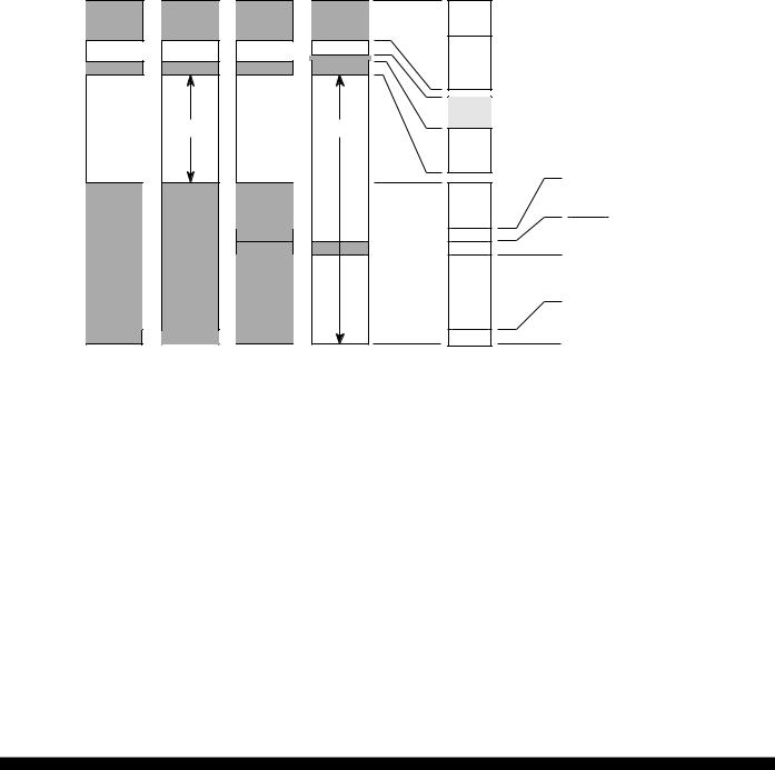
The INIT, INIT2, and CONFIG registers control the presence and location of the registers, RAM, EEPROM, and ROM/EPROM in the 64 Kbyte CPU address space. The 128-byte register block originates at $0000 after reset and can be placed at any 4 Kbyte boundary ($x000) after reset by writing an appropriate value to the INIT register. Refer to Figure 4.
$0000 |
|
|
|
x000 |
|
|
|
|
x07F |
|
EXT |
|
EXT |
x080 |
$1000 |
|
|
|
x37F |
|
|
|
|
xD00 |
|
EXT |
|
EXT |
xD7F |
|
|
xD80 |
||
|
|
|
|
|
|
|
|
|
xFFF |
$A000 |
|
|
|
A000 |
$FFFF |
|
|
|
FFFF |
SINGLE |
EXPANDED |
BOOTSTRAP |
SPECIAL |
|
CHIP |
|
|
TEST |
|
128-BYTE REGISTER BLOCK (CAN BE REMAPPED TO ANY
4K PAGE BY THE INIT REGISTER)
768 BYTES RAM
(CAN BE REMAPPED TO ANY
4K PAGE BY THE INIT REGISTER)
RESERVED (SPECIAL TEST MODE ONLY)
640 BYTES EEPROM
(CAN BE REMAPPED TO ANY
4K PAGE BY THE INIT2 REGISTER)
|
BOOT ROM |
|
BE00 |
||
(ONLY PRESENT IN |
||
|
||
|
BOOTSTRAP MODE) |
|
BFC0 |
SPECIAL MODE |
|
BFFF |
INTERRUPT |
|
VECTORS |
24 KBYTES ROM/EPROM
(CAN BE REMAPPED TO $2000–$7FFF OR $A000–$FFFF BY THE CONFIG REGISTER)
FFC0 |
NORMAL MODE |
FFFF |
INTERRUPT |
VECTORS |
NOTE: ROM/EPROM can be enabled in special test mode by setting ROMON bit in the config register after reset.
Figure 4 Memory Map
MOTOROLA |
M68HC11 K Series |
14 |
MC6HC11KTS/D |

|
INIT = $00 |
|
|
INIT = $10 |
|
INIT = $04 |
|
|
|
|
|
|
|
|
|
|
|
|
REG @ $0000 |
|
|
REG @ $0000 |
|
REG @ $4000 |
|
|
|
RAM @ $0080 |
|
|
RAM @ $1000 |
|
RAM @ $0000 |
|
|
|
|
|
|
|
|
|
|
|
|
$0000 |
|
|
$0000 |
|
|
$0000 |
|
|
REGISTER |
|
|
REGISTER |
|
|
RAM |
|
|
BLOCK |
|
|
BLOCK |
|
|
A |
|
|
$007F |
|
|
$007F |
|
|
$007F |
|
|
|
|
|
|
|
|
|
|
|
$0080 |
|
|
|
|
|
$0080 |
|
|
|
|
|
|
|
|
||
|
|
|
|
|
|
|
|
|
|
|
|
|
$1000 |
|
|
|
|
|
RAM |
|
|
RAM |
|
|
RAM |
|
|
|
|
A |
|
|
|
||
|
B |
|
|
|
|
B |
|
|
|
|
|
$107F |
|
|
|
||
|
|
|
|
|
|
|
|
|
|
|
|
|
|
|
|
|
|
|
|
|
|
$1080 |
|
|
|
|
|
$02FF |
|
|
|
|
|
$02FF |
|
|
|
|
|
|
|
|
|
|
|
$0300 |
|
|
RAM |
|
|
|
|
|
|
|
|
|
|
|
||
|
|
|
|
|
|
|
|
|
|
RAM |
|
|
B |
|
|
$4000 |
|
|
|
|
|
|
|
REGISTER |
|
|
|
A |
|
|
|
|
|
|
|
|
|
|
|
|
|
|
BLOCK |
|
|
$037F |
|
|
$12FF |
|
|
$407F |
|
|
|
|
|
|
|
|
|
|
|
|
|
|
|
|
|
|
|
Figure 5 RAM and Register Mapping
Table 4 M68HC11 K Series Register and Control Bit Assignments
(Can be remapped to any 4-Kbyte boundary)
|
Bit 7 |
6 |
5 |
4 |
3 |
2 |
1 |
Bit 0 |
|
$0000 |
PA7 |
PA6 |
PA5 |
PA4 |
PA3 |
PA2 |
PA1 |
PA0 |
PORTA |
|
|
|
|
|
|
|
|
|
|
$0001 |
DDA7 |
DDA6 |
DDA5 |
DDA4 |
DDA3 |
DDA2 |
DDA1 |
DDA0 |
DDRA |
|
|
|
|
|
|
|
|
|
|
$0002 |
DDB7 |
DDB6 |
DDB5 |
DDB4 |
DDB3 |
DDB2 |
DDB1 |
DDB0 |
DDRB |
|
|
|
|
|
|
|
|
|
|
$0003 |
DDF7 |
DDF6 |
DDF5 |
DDF4 |
DDF3 |
DDF2 |
DDF1 |
DDF0 |
DDRF |
|
|
|
|
|
|
|
|
|
|
$0004 |
PB7 |
PB6 |
PB5 |
PB4 |
PB3 |
PB2 |
PB1 |
PB0 |
PORTB |
|
|
|
|
|
|
|
|
|
|
$0005 |
PF7 |
PF6 |
PF5 |
PF4 |
PF3 |
PF2 |
PF1 |
PF0 |
PORTF |
|
|
|
|
|
|
|
|
|
|
$0006 |
PC7 |
PC6 |
PC5 |
PC4 |
PC3 |
PC2 |
PC1 |
PC0 |
PORTC |
|
|
|
|
|
|
|
|
|
|
$0007 |
DDC7 |
DDC6 |
DDC5 |
DDC4 |
DDC3 |
DDC2 |
DDC1 |
DDC0 |
DDRC |
|
|
|
|
|
|
|
|
|
|
$0008 |
0 |
0 |
PD5 |
PD4 |
PD3 |
PD2 |
PD1 |
PD0 |
PORTD |
|
|
|
|
|
|
|
|
|
|
$0009 |
0 |
0 |
DDD5 |
DDD4 |
DDD3 |
DDD2 |
DDD1 |
DDD0 |
DDRD |
|
|
|
|
|
|
|
|
|
|
$000A |
PE7 |
PE6 |
PE5 |
PE4 |
PE3 |
PE2 |
PE1 |
PE0 |
PORTE |
|
|
|
|
|
|
|
|
|
|
$000B |
FOC1 |
FOC2 |
FOC3 |
FOC4 |
FOC5 |
0 |
0 |
0 |
CFORC |
|
|
|
|
|
|
|
|
|
|
$000C |
OC1M7 |
OC1M6 |
OC1M5 |
OC1M4 |
OC1M3 |
0 |
0 |
0 |
OC1M |
|
|
|
|
|
|
|
|
|
|
$000D |
OC1D7 |
OC1D6 |
OC1D5 |
OC1D4 |
OC1D3 |
0 |
0 |
0 |
OC1D |
|
|
|
|
|
|
|
|
|
|
$000E |
Bit 15 |
14 |
13 |
12 |
11 |
10 |
9 |
Bit 8 |
TCNT (High) |
|
|
|
|
|
|
|
|
|
|
$000F |
Bit 7 |
6 |
5 |
4 |
3 |
2 |
1 |
Bit 0 |
TCNT (Low) |
|
|
|
|
|
|
|
|
|
|
$0010 |
Bit 15 |
14 |
13 |
12 |
11 |
10 |
9 |
Bit 8 |
TIC1 (High) |
|
|
|
|
|
|
|
|
|
|
$0011 |
Bit 7 |
6 |
5 |
4 |
3 |
2 |
1 |
Bit 0 |
TIC1 (Low) |
|
|
|
|
|
|
|
|
|
|
$0012 |
Bit 15 |
14 |
13 |
12 |
11 |
10 |
9 |
Bit 8 |
TIC2 (High) |
|
|
|
|
|
|
|
|
|
|
$0013 |
Bit 7 |
6 |
5 |
4 |
3 |
2 |
1 |
Bit 0 |
TIC2 (Low) |
|
|
|
|
|
|
|
|
|
|
$0014 |
Bit 15 |
14 |
13 |
12 |
11 |
10 |
9 |
Bit 8 |
TIC3 (High) |
|
|
|
|
|
|
|
|
|
|
|
|
|
|
|
|
|
|
|
|
|
|
|
|
|
|
|
|
|
|
M68HC11 K Series |
MOTOROLA |
MC6HC11KTS/D |
15 |
Table 4 M68HC11 K Series Register and Control Bit Assignments (Continued)
(Can be remapped to any 4-Kbyte boundary)
|
Bit 7 |
6 |
5 |
4 |
3 |
2 |
1 |
Bit 0 |
|
$0015 |
Bit 7 |
6 |
5 |
4 |
3 |
2 |
1 |
Bit 0 |
TIC3 (Low) |
|
|
|
|
|
|
|
|
|
|
$0016 |
Bit 15 |
14 |
13 |
12 |
11 |
10 |
9 |
Bit 8 |
TOC1(High) |
|
|
|
|
|
|
|
|
|
|
$0017 |
Bit 7 |
6 |
5 |
4 |
3 |
2 |
1 |
Bit 0 |
TOC1 (Low) |
|
|
|
|
|
|
|
|
|
|
$0018 |
Bit 15 |
14 |
13 |
12 |
11 |
10 |
9 |
Bit 8 |
TOC2 (High) |
|
|
|
|
|
|
|
|
|
|
$0019 |
Bit 7 |
6 |
5 |
4 |
3 |
2 |
1 |
Bit 0 |
TOC2 (Low) |
|
|
|
|
|
|
|
|
|
|
$001A |
Bit 15 |
14 |
13 |
12 |
11 |
10 |
9 |
Bit 8 |
TOC3 (High) |
|
|
|
|
|
|
|
|
|
|
$001B |
Bit 7 |
6 |
5 |
4 |
3 |
2 |
1 |
Bit 0 |
TOC3 (Low) |
|
|
|
|
|
|
|
|
|
|
$001C |
Bit 15 |
14 |
13 |
12 |
11 |
10 |
9 |
Bit 8 |
TOC4 (High) |
|
|
|
|
|
|
|
|
|
|
$001D |
Bit 7 |
6 |
5 |
4 |
3 |
2 |
1 |
Bit 0 |
TOC4 (Low) |
|
|
|
|
|
|
|
|
|
|
$001E |
Bit 15 |
14 |
13 |
12 |
11 |
10 |
9 |
Bit 8 |
TI4/O5 (High) |
|
|
|
|
|
|
|
|
|
|
$001F |
Bit 7 |
6 |
5 |
4 |
3 |
2 |
1 |
Bit 0 |
TI4/O5 (Low) |
|
|
|
|
|
|
|
|
|
|
$0020 |
OM2 |
OL2 |
OM3 |
OL3 |
OM4 |
OL4 |
OM5 |
OL5 |
TCTL1 |
|
|
|
|
|
|
|
|
|
|
$0021 |
EDG4B |
EDG4A |
EDG1B |
EDG1A |
EDG2B |
EDG2A |
EDG3B |
EDG3A |
TCTL2 |
|
|
|
|
|
|
|
|
|
|
$0022 |
OC1I |
OC2I |
OC3I |
OC4I |
I4/O5I |
IC1I |
IC2I |
IC3I |
TMSK1 |
|
|
|
|
|
|
|
|
|
|
$0023 |
OC1F |
OC2F |
OC3F |
OC4F |
I4/O5F |
IC1F |
IC2F |
IC3F |
TFLG1 |
|
|
|
|
|
|
|
|
|
|
$0024 |
TOI |
RTII |
PAOVI |
PAII |
0 |
0 |
PR1 |
PR0 |
TMSK2 |
|
|
|
|
|
|
|
|
|
|
$0025 |
TOF |
RTIF |
PAOVF |
PAIF |
0 |
0 |
0 |
0 |
TFLG2 |
|
|
|
|
|
|
|
|
|
|
$0026 |
0 |
PAEN |
PAMOD |
PEDGE |
0 |
I4/O5 |
RTR1 |
RTR0 |
PACTL |
|
|
|
|
|
|
|
|
|
|
$0027 |
Bit 7 |
6 |
5 |
4 |
3 |
2 |
1 |
Bit 0 |
PACNT |
|
|
|
|
|
|
|
|
|
|
$0028 |
SPIE |
SPE |
DWOM |
MSTR |
CPOL |
CPHA |
SPR1 |
SPR0 |
SPCR |
|
|
|
|
|
|
|
|
|
|
$0029 |
SPIF |
WCOL |
0 |
MODF |
0 |
0 |
0 |
Bit 0 |
SPSR |
|
|
|
|
|
|
|
|
|
|
$002A |
Bit 7 |
6 |
5 |
4 |
3 |
2 |
1 |
Bit 0 |
SPDR |
|
|
|
|
|
|
|
|
|
|
$002B |
MBE |
0 |
ELAT |
EXCOL |
EXROW |
T1 |
T0 |
EPGM |
EPROG* |
|
|
|
|
|
|
|
|
|
|
$002C |
0 |
0 |
0 |
0 |
HPPUE |
GPPUE |
FPPUE |
BPPUE |
PPAR |
|
|
|
|
|
|
|
|
|
|
$002D |
0 |
0 |
PGAR5 |
PGAR4 |
PGAR3 |
PGAR2 |
PGAR1 |
PGAR0 |
PGAR |
$002E |
|
|
|
|
|
|
|
|
Reserved |
|
|
|
|
|
|
|
|
||
$002F |
|
|
|
|
|
|
|
|
Reserved |
|
|
|
|
|
|
|
|
||
|
|
|
|
|
|
|
|
|
|
$0030 |
CCF |
0 |
SCAN |
MULT |
CD |
CC |
CB |
CA |
ADCTL |
|
|
|
|
|
|
|
|
|
|
$0031 |
Bit 7 |
6 |
5 |
4 |
3 |
2 |
1 |
Bit 0 |
ADR1 |
|
|
|
|
|
|
|
|
|
|
$0032 |
Bit 7 |
6 |
5 |
4 |
3 |
2 |
1 |
Bit 0 |
ADR2 |
|
|
|
|
|
|
|
|
|
|
$0033 |
Bit 7 |
6 |
5 |
4 |
3 |
2 |
1 |
Bit 0 |
ADR3 |
|
|
|
|
|
|
|
|
|
|
$0034 |
Bit 7 |
6 |
5 |
4 |
3 |
2 |
1 |
Bit 0 |
ADR4 |
|
|
|
|
|
|
|
|
|
|
$0035 |
BULKP |
LVPEN |
BPRT4 |
PTCON |
BPRT3 |
BPRT2 |
BPRT1 |
BPRT0 |
BPROT |
$0036 |
|
|
|
|
|
|
|
|
Reserved |
|
|
|
|
|
|
|
|
||
|
|
|
|
|
|
|
|
|
|
$0037 |
EE3 |
EE2 |
EE1 |
EE0 |
0 |
0 |
0 |
0 |
INIT2 |
|
|
|
|
|
|
|
|
|
|
$0038 |
LIRDV |
CWOM |
0 |
IRVNE |
LSBF |
SPR2 |
XDV1 |
XDV0 |
OPT2 |
|
|
|
|
|
|
|
|
|
|
$0039 |
ADPU |
CSEL |
IRQE |
DLY |
CME |
FCME |
CR1 |
CR0 |
OPTION |
|
|
|
|
|
|
|
|
|
|
$003A |
Bit 7 |
6 |
5 |
4 |
3 |
2 |
1 |
Bit 0 |
COPRST |
|
|
|
|
|
|
|
|
|
|
$003B |
ODD |
EVEN |
LVPI |
BYTE |
ROW |
ERASE |
EELAT |
EEPGM |
PPROG |
|
|
|
|
|
|
|
|
|
|
$003C |
RBOOT |
SMOD |
MDA |
PSEL4 |
PSEL3 |
PSEL2 |
PSEL1 |
PSEL0 |
HPRIO |
|
|
|
|
|
|
|
|
|
|
$003D |
RAM3 |
RAM2 |
RAM1 |
RAM0 |
REG3 |
REG2 |
REG1 |
REG0 |
INIT |
|
|
|
|
|
|
|
|
|
|
$003E |
TILOP |
0 |
OCCR |
CBYP |
DISR |
FCM |
FCOP |
0 |
TEST1 |
|
|
|
|
|
|
|
|
|
|
$003F |
ROMAD |
1 |
CLKX |
PAREN |
NOSEC |
NOCOP |
ROMON |
EEON |
CONFIG |
$0040 |
|
|
|
|
|
|
|
|
Reserved |
|
|
|
|
|
|
|
|
||
to |
|
|
|
|
|
|
|
|
|
|
|
|
|
|
|
|
|
|
|
$0055 |
|
|
|
|
|
|
|
|
Reserved |
|
|
|
|
|
|
|
|
||
|
|
|
|
|
|
|
|
|
|
$0056 |
MXGS2 |
MXGS1 |
W2SZ1 |
W2SZ0 |
0 |
0 |
W1SZ1 |
W1SZ0 |
MMSIZ |
|
|
|
|
|
|
|
|
|
|
$0057 |
W2A15 |
W2A14 |
W2A13 |
0 |
W1A15 |
W1A14 |
W1A13 |
0 |
MMWBR |
|
|
|
|
|
|
|
|
|
|
|
|
|
|
|
|
|
|
|
|
|
|
|
|
|
|
|
|
|
|
MOTOROLA |
M68HC11 K Series |
16 |
MC6HC11KTS/D |

Table 4 M68HC11 K Series Register and Control Bit Assignments (Continued)
(Can be remapped to any 4-Kbyte boundary)
|
Bit 7 |
6 |
5 |
4 |
3 |
2 |
1 |
Bit 0 |
|
$0058 |
0 |
X1A18 |
X1A17 |
X1A16 |
X1A15 |
X1A14 |
X1A13 |
0 |
MM1CR |
|
|
|
|
|
|
|
|
|
|
$0059 |
0 |
X2A18 |
X2A17 |
X2A16 |
X2A15 |
X2A14 |
X2A13 |
0 |
MM2CR |
|
|
|
|
|
|
|
|
|
|
$005A |
IOSA |
IOSB |
GP1SA |
GP1SB |
GP2SA |
GP2SB |
PCSA |
PCSB |
CSCSTR |
|
|
|
|
|
|
|
|
|
|
$005B |
IOEN |
IOPL |
IOCSA |
IOSZ |
GCSPR |
PCSEN |
PCSZA |
PCSZB |
CSCTL |
|
|
|
|
|
|
|
|
|
|
$005C |
G1A18 |
G1A17 |
G1A16 |
G1A15 |
G1A14 |
G1A13 |
G1A12 |
G1A11 |
GPCS1A |
|
|
|
|
|
|
|
|
|
|
$005D |
G1DG2 |
G1DPC |
G1POL |
G1AV |
G1SZA |
G1SZB |
G1SZC |
G1SZD |
GPCS1C |
|
|
|
|
|
|
|
|
|
|
$005E |
G2A18 |
G2A17 |
G2A16 |
G2A15 |
G2A14 |
G2A13 |
G2A12 |
G2A11 |
GPCS2A |
|
|
|
|
|
|
|
|
|
|
$005F |
0 |
G2DPC |
G2POL |
G2AV |
G2SZA |
G2SZB |
G2SZC |
G2SZD |
GPCS2C |
|
|
|
|
|
|
|
|
|
|
$0060 |
CON34 |
CON12 |
PCKA2 |
PCKA1 |
0 |
PCKB3 |
PCKB2 |
PCKB1 |
PWCLK |
|
|
|
|
|
|
|
|
|
|
$0061 |
PCLK4 |
PCLK3 |
PCLK2 |
PCLK1 |
PPOL4 |
PPOL3 |
PPOL2 |
PPOL1 |
PWPOL |
|
|
|
|
|
|
|
|
|
|
$0062 |
Bit 7 |
6 |
5 |
4 |
3 |
2 |
1 |
Bit 0 |
PWSCAL |
|
|
|
|
|
|
|
|
|
|
$0063 |
TPWSL |
DISCP |
0 |
0 |
PWEN4 |
PWEN3 |
PWEN2 |
PWEN1 |
PWEN |
|
|
|
|
|
|
|
|
|
|
$0064 |
Bit 7 |
6 |
5 |
4 |
3 |
2 |
1 |
Bit 0 |
PWCNT1 |
|
|
|
|
|
|
|
|
|
|
$0065 |
Bit 7 |
6 |
5 |
4 |
3 |
2 |
1 |
Bit 0 |
PWCNT2 |
|
|
|
|
|
|
|
|
|
|
$0066 |
Bit 7 |
6 |
5 |
4 |
3 |
2 |
1 |
Bit 0 |
PWCNT3 |
|
|
|
|
|
|
|
|
|
|
$0067 |
Bit 7 |
6 |
5 |
4 |
3 |
2 |
1 |
Bit 0 |
PWCNT4 |
|
|
|
|
|
|
|
|
|
|
$0068 |
Bit 7 |
6 |
5 |
4 |
3 |
2 |
1 |
Bit 0 |
PWPER1 |
|
|
|
|
|
|
|
|
|
|
$0069 |
Bit 7 |
6 |
5 |
4 |
3 |
2 |
1 |
Bit 0 |
PWPER2 |
|
|
|
|
|
|
|
|
|
|
$006A |
Bit 7 |
6 |
5 |
4 |
3 |
2 |
1 |
Bit 0 |
PWPER3 |
|
|
|
|
|
|
|
|
|
|
$006B |
Bit 7 |
6 |
5 |
4 |
3 |
2 |
1 |
Bit 0 |
PWPER4 |
|
|
|
|
|
|
|
|
|
|
$006C |
Bit 7 |
6 |
5 |
4 |
3 |
2 |
1 |
Bit 0 |
PWDTY1 |
|
|
|
|
|
|
|
|
|
|
$006D |
Bit 7 |
6 |
5 |
4 |
3 |
2 |
1 |
Bit 0 |
PWDTY2 |
|
|
|
|
|
|
|
|
|
|
$006E |
Bit 7 |
6 |
5 |
4 |
3 |
2 |
1 |
Bit 0 |
PWDTY3 |
|
|
|
|
|
|
|
|
|
|
$006F |
Bit 7 |
6 |
5 |
4 |
3 |
2 |
1 |
Bit 0 |
PWDTY4 |
|
|
|
|
|
|
|
|
|
|
$0070 |
BTST |
BSPL |
0 |
SBR12 |
SBR11 |
SBR10 |
SBR9 |
SBR8 |
SCBDH |
|
|
|
|
|
|
|
|
|
|
$0071 |
SBR7 |
SBR6 |
SBR5 |
SBR4 |
SBR3 |
SBR2 |
SBR1 |
SBR0 |
SCBDL |
|
|
|
|
|
|
|
|
|
|
$0072 |
LOOPS |
WOMS |
0 |
M |
WAKE |
ILT |
PE |
PT |
SCCR1 |
|
|
|
|
|
|
|
|
|
|
$0073 |
TIE |
TCIE |
RIE |
ILIE |
TE |
RE |
RWU |
SBK |
SCCR2 |
|
|
|
|
|
|
|
|
|
|
$0074 |
TDRE |
TC |
RDRF |
IDLE |
OR |
NF |
FE |
PF |
SCSR1 |
|
|
|
|
|
|
|
|
|
|
$0075 |
0 |
0 |
0 |
0 |
0 |
0 |
0 |
RAF |
SCSR2 |
|
|
|
|
|
|
|
|
|
|
$0076 |
R8 |
T8 |
0 |
0 |
0 |
0 |
0 |
0 |
SCDRH |
|
|
|
|
|
|
|
|
|
|
$0077 |
R7/T7 |
R6/T6 |
R5/T5 |
R4/T4 |
R3/T3 |
R2/T2 |
R1/T1 |
R0/T0 |
SCDRL |
$0078 |
|
|
|
|
|
|
|
|
Reserved |
|
|
|
|
|
|
|
|
||
to |
|
|
|
|
|
|
|
|
|
|
|
|
|
|
|
|
|
|
|
$007B |
|
|
|
|
|
|
|
|
Reserved |
|
|
|
|
|
|
|
|
||
|
|
|
|
|
|
|
|
|
|
$007C |
PH7 |
PH6 |
PH5 |
PH4 |
PH3 |
PH2 |
PH1 |
PH0 |
PORTH |
|
|
|
|
|
|
|
|
|
|
$007D |
DDH7 |
DDH6 |
DDH5 |
DDH4 |
DDH3 |
DDH2 |
DDH1 |
DDH0 |
DDRH |
|
|
|
|
|
|
|
|
|
|
$007E |
PG7 |
PG6 |
PG5 |
PG4 |
PG3 |
PG2 |
PG1 |
PG0 |
PORTG |
|
|
|
|
|
|
|
|
|
|
$007F |
DDG7 |
DDG6 |
DDG5 |
DDG4 |
DDG3 |
DDG2 |
DDG1 |
DDG0 |
DDRG |
|
|
|
|
|
|
|
|
|
|
*MC68HC711K4 only.
3.2 RAM
All members of the M68HC11 K series have 768 bytes of static RAM. The RAM can be mapped to any 4-Kbyte boundary. Upon reset, the RAM is mapped at $0080–$037F. The registers are also mapped to this 4-Kbyte boundary. In previous versions of the M68HC11 devices the register block being mapped to the same boundary would cause the portion of RAM overlapped by the register block to be lost. However, a new RAM remapping feature has been added which automatically allows all of the RAM to be accessible even if the register block overlaps the RAM. Because the registers are located in the same
M68HC11 K Series |
MOTOROLA |
MC6HC11KTS/D |
17 |

4-Kbyte boundary after reset, 128 bytes of the RAM are located at $0300 to $037F. Remapping is accomplished by writing appropriate values to the INIT register. Refer to the register and RAM mapping examples following the memory map diagram.
When power is removed from the MCU, RAM contents may be preserved using the MODB/VSTBY pin. A power source (2.0 Vdc –VDD) applied to this pin protects all 768 bytes of RAM.
INIT — RAM and Register Mapping |
|
|
|
|
$003D |
|||
|
Bit 7 |
6 |
5 |
4 |
3 |
2 |
1 |
Bit 0 |
|
|
|
|
|
|
|
|
|
|
RAM3 |
RAM2 |
RAM1 |
RAM0 |
REG3 |
REG2 |
REG1 |
REG0 |
|
|
|
|
|
|
|
|
|
RESET: |
0 |
0 |
0 |
0 |
0 |
0 |
0 |
0 |
Can be written only once in first 64 cycles out of reset in normal modes or at any time in special mode.
RAM[3:0] —Internal RAM Map Position
These bits determine the upper four bits of the RAM address. At reset RAM is mapped to $0000. Normally the RAM would be mapped at $0000–$02FF (768 bytes). However, the register block overlaps the first 128 bytes of RAM, causing them to be remapped to $0300–$037F. Refer to Figure 4 and Figure 5.
REG[3:0] —128-Byte Register Block Map Position
These bits determine the upper four bits of the register block starting address. At reset registers are mapped to $0000 and overlap the first 128 bytes of RAM, causing them to be remapped to $0300– $037F. Refer to Figure 4 and Figure 5.
3.3 ROM/EPROM
Standard devices have 24 kbytes of EPROM (OTPROM in a non-windowed package). Custom ROM devices have a 24-Kbyte ROM array that is mask programmed at the factory to customer specifications. The MC68HC11K0, MC68HC11K1, MC68L11K0, and MC68L11K1 have no ROM/EPROM. Refer to the ordering information tables.
The ROMAD and ROMON control bits in the CONFIG register control the position and presence of ROM/EPROM in the memory map. The ROM/EPROM can be mapped at $2000–$7FFF or $A000– $FFFF. If it is mapped to $A000–$FFFF, vector space is included. In single-chip mode the ROM/ EPROM is forced to $A000–$FFFF (ROMAD = 1) and enabled (ROMON = 1), regardless of the value in the CONFIG register. This ensures that there will be ROM/EPROM at the vector space. In special test mode, the ROMON bit is forced to zero so that the ROM/EPROM is removed from the memory map. Refer to Figure 4.
Programming EPROM requires an external 12.25 volt nominal power supply (VPPE) that must be ap-
plied to the XIRQ/VPPE pin. Three methods are used to program and verify EPROM/OTPROM.
Normal EPROM/OTPROM programming can be accomplished in any operating mode. Normal programming is accomplished using the EPROM/OTPROM programming register (EPROG). The EPROG register enables the EPROM programming voltage, controls the latching of data to be programmed, and selects singleor multiple-byte programming.
To program the EPROM, complete the following steps using the EPROG register:
1.Set the ELAT bit in EPROG register. EELAT bit in PPROG must be cleared as it negates the function of the ELAT bit.
2.Write data to the desired address.
3.Turn on programming voltage to the EPROM array by setting the EPGM bit in EPROG register.
4.Delay for 2 ms or more, as appropriate.
5.Clear the EPGM bit in EPROG to turn off the programming voltage.
MOTOROLA |
M68HC11 K Series |
18 |
MC6HC11KTS/D |

6.Clear the EPROG register to reconfigure the EPROM address and data buses for normal operation.
In EPROM emulation mode (PROG mode), the EPROM/OTPROM is programmed as a stand-alone EPROM by adapting the MCU footprint to the 27C256-type EPROM and using an appropriate EPROM programmer. To put the MCU in PROG mode, pull the following pins low: MODA/LIR, MODB/VSTBY,
RESET, PA[2:0]. Refer to Figure 6.
In the third method, the EPROM is programmed by software while in the special test or bootstrap modes. User-developed software can be uploaded through the SCI, or a ROM resident EPROM programming utility can be used. To use the resident utility, bootload a three-byte program consisting of a single jump instruction to $BF00. $BF00 is the starting address of a resident EPROM programming utility. The utility program sets the X and Y index registers to default values, then receives programming data from an external host and programs it into EPROM. The value in IX determines programming delay time. The value in IY is a pointer to the first address in EPROM to be programmed (default = $A000).
When the utility program is ready to receive programming data, it sends the host the $FF character. Then it waits. When the host sees the $FF character, the EPROM programming data is sent, starting with the first location in the EPROM array. After the last byte to be programmed is sent and the corresponding verification data is returned, the programming operation is terminated by resetting the MCU.
Although the external 12.25 V programming voltage must be applied to the XIRQ/VPPE pin during EPROM programming, it should be equal to VDD before verifying the data that was just programmed. It
should equal VDD during normal operation also. The XIRQ/VPPE pin has a high voltage detect circuit that inhibits assertion of the ELAT bit when programming voltage is at low levels.
CAUTION
If the MCU is used in any operating mode while high voltage (12.25 V nominal) is present on the XIRQ/VPPE pin, the IRQ/CE pin must be pulled high to avoid accidental programming or corruption of EPROM contents. After programming an EPROM location, IRQ pin must also be pulled high before the address and data are changed to program the next location.
EPROG — EPROM Programming Control |
|
|
|
|
|
|
$002B |
|||
|
Bit 7 |
6 |
5 |
4 |
3 |
|
2 |
1 |
|
Bit 0 |
|
|
|
|
|
|
|
|
|
|
|
|
MBE |
— |
ELAT |
EXCOL |
EXROW |
— |
|
— |
|
EPGM |
|
|
|
|
|
|
|
|
|
|
|
RESET: |
0 |
0 |
0 |
0 |
0 |
|
0 |
0 |
0 |
|
MBE —Multiple-Byte Programming Enable
0 = EPROM array configured for normal programming
1 = Program two bytes with the same data
When multiple-byte programming is enabled, address bit 5 is considered a don't care so that bytes with address bit 5 = 0 and address bit 5 = 1 both get programmed. MBE can be read in any mode and always reads zero in normal modes. MBE can only be written in special modes.
Bit 6 —Not implemented
Always reads zero
ELAT —EPROM Latch Control
ELAT can be read any time. ELAT can be written any time except when EPGM = 1, then the write to ELAT will be disabled. When ELAT = 1, writes to EPROM cause address and data to be latched and the EPROM cannot be read.
0 = EPROM address and data bus configured for normal reads 1 = EPROM address and data bus configured for programming
M68HC11 K Series |
MOTOROLA |
MC6HC11KTS/D |
19 |

EXCOL —Select Extra Columns 0 = User array selected
1 = User array is disabled and extra columns are accessed at bits [7:0]. Addresses use bits [11:5] and bits [4:0] are don't care. EXCOL can only be read in special modes and always returns zero in normal modes. EXCOL can be written in special modes only.
EXROW —Select Extra Rows
0 = User array selected
1 = User array is disabled and two extra rows are available. Addresses use bits [5:0] and bits [11:6] are don't care. EXROW can only be read in special modes and always returns zero in normal modes. EXROW can be written in special modes only.
Bits [2:1] —Not implemented
Always read zero
EPGM —EPROM Programming Voltage Enable
EPGM can be read any time and can only be written when ELAT = 1. 0 = Programming voltage to EPROM array disconnected
1 = Programming voltage to EPROM array connected
MOTOROLA |
M68HC11 K Series |
20 |
MC6HC11KTS/D |
 EPROM MODE PIN CONNECTIONS
 MCU PIN FUNCTIONS
EPROM
PIN FUNCTIONS
ADDR0 |
PF0/ADDR0 |
ADDR0 |
ADDR1 |
PF1/ADDR1 |
ADDR1 |
ADDR2 |
PF2/ADDR2 |
ADDR2 |
ADDR3 |
PF3/ADDR3 |
ADDR3 |
ADDR4 |
PF4/ADDR4 |
ADDR4 |
ADDR5 |
PF5/ADDR5 |
ADDR5 |
ADDR6 |
PF6/ADDR6 |
ADDR6 |
ADDR7 |
PF7/ADDR7 |
ADDR7 |
ADDR8 |
PB0/ADDR8 |
ADDR8 |
ADDR9 |
PB1/ADDR9 |
ADDR9 |
ADDR10 |
PB2/ADDR10 |
ADDR10 |
ADDR11 |
PB3/ADDR11 |
ADDR11 |
ADDR12 |
PB4/ADDR12 |
ADDR12 |
ADDR13 |
PB5/ADDR13 |
ADDR13 |
ADDR14 |
PB6/ADDR14 |
ADDR14 |
|
|
|
GND |
PA0/IC3 |
NOTE 4 |
GND |
PA1/IC2 |
||
|
|
|
GND |
PA2/IC1 |
|
|
|
|
|
|
|
|
GND |
PA3/IC4/OC5/OC1 |
|
|
|
|
GND |
PA4/OC4/OC1 |
|
|
|
|
GND |
PA5/OC3/OC1 |
|
|
|
|
GND |
PA6/OC2/OC1 |
|
|
|
|
GND |
PA7/PAI/OC1 |
|
|
|
|
GND |
PG0/XA13 |
|
|
|
|
GND |
PG1/XA14 |
|
|
|
|
GND |
PG2/XA15 |
|
|
|
|
GND |
PG3/XA16 |
|
NOTE 1 |
GND |
PG4/XA17 |
|||
|
|
|
GND |
PG5/XA18 |
|
|
|
|
GND |
|
PG6 |
|
|
|
GND |
PG7/R/W |
|
|
|
|
GND |
PD0/RxD |
|
|
|
|
GND |
PD1/TxD |
|
|
|
|
GND |
PD2/MISO |
|
|
|
|
GND |
PD3/MOSI |
|
|
|
|
GND |
PD4/SCK |
|
|
|
|
GND |
|
PD5/SS |
|
|
|
|
|
|
INTERNAL 24 KBYTE EPROM
MC68HC711K4
O0 |
PC0/DATA0 |
|
O0 |
|||
O1 |
PC1/DATA1 |
|
O1 |
|||
O2 |
PC2/DATA2 |
|
O2 |
|||
O3 |
PC3/DATA3 |
|
O3 |
|||
O4 |
PC4/DATA4 |
|
O4 |
|||
O5 |
PC5/DATA5 |
|
O5 |
|||
O6 |
PC6/DATA6 |
|
O6 |
|||
O7 |
PC7/DATA7 |
|
O7 |
|||
|
|
|
PB7/ADDR15 |
|
|
|
OE |
|
OE |
||||
CE |
IRQ |
|
|
CE |
||
VPP |
XIRQ/VPPE |
VPP |
||||
VCC |
VDD |
VCC |
||||
VSS |
VSS |
VSS |
||||
|
|
|
PE0/AN0 |
|
|
|
|
|
|
PE1/AN1 |
|
|
|
|
|
|
PE2/AN2 |
UNUSED |
||
|
|
|
PE3/AN3 |
|||
|
|
|
PE4/AN4 |
INPUTS |
||
|
|
|
PE5/AN5 |
|
|
|
|
|
|
PE6/AN6 |
|
|
|
|
|
|
PE7/AN7 |
|
|
|
PH0/PW1 GND
PH1/PW2 GND
PH2/PW3 GND
PH3/PW4 GND
PH4/CSIO GND
PH5/CSGP1 GND
PH6/CSGP2 GND
PH7/CSPROG GND
VRL |
GND |
VRH |
GND |
EXTAL |
GND |
XTAL |
UNUSED |
XOUT |
|
E |
OUTPUTS |
TESTxx (3) |
|
MODA/LIR GND
MODB/VSTBY GND
RESET GND
NOTES:
1.Unused Inputs – grounding is recommended.
2.Unused Inputs – these pins may be left unterminated.
3.Unused Outputs – these pins should be left unconnected.
4.Grounding these six pins configures the MC68HC711K4 for EPROM emulation mode.
NOTE 2
NOTE 1
NOTE 3
NOTE 4
Figure 6 Pin Assignments of the MC68HC711K4 MCU in PROG Mode
M68HC11 K Series |
MOTOROLA |
MC6HC11KTS/D |
21 |

3.4 EEPROM
The 640-byte EEPROM is initially located at $0D80 after reset, assuming EEPROM is enabled in the memory map by the EEON bit in the CONFIG register. EEPROM can be placed at any 4-Kbyte boundary ($xD80) by writing appropriate values to the INIT2 register. Note that EEPROM can be mapped so that it contains the vector space. Refer to Figure 4. The MC68HC11K0, MC68HC11K3, MC68L11K0, and MC68L11K3 have no EEPROM. Refer to the ordering information tables.
Programming and erasing the EEPROM is controlled by the PPROG register, and dependent upon the block protect (BPROT) register value. An on-chip charge pump develops the high voltage required for programming and erasing. When the frequency of the E clock is less than 1 MHz, select the internal clock source to drive the EEPROM charge pump by writing one to the CSEL bit in the OPTION register.
The CONFIG register consists of a single EEPROM byte. Although the byte is not included in the 640byte EEPROM array, programming the CONFIG register requires the same procedure as any byte in the array. The erased state of bits in the CONFIG register is logic one. Refer to the CONFIG register description that follows this section.
The erased state of an EEPROM byte is $FF (all ones).
To erase the EEPROM, ensure that the proper bits of the BPROT register are cleared, then complete the following steps using the PPROG register:
1.Set the ERASE, EELAT, and appropriate BYTE and ROW bits in PPROG register.
2.Write to the appropriate EEPROM address with any data. Row erase only requires a write to any location in the row. Bulk erase is done by writing to any location in the array.
3.Set the ERASE, EELAT, EEPGM, and appropriate BYTE and ROW bits in PPROG register.
4.Delay for 10 ms or more, as appropriate.
5.Clear the EEPGM bit in PPROG to turn off the programming voltage.
6.Clear the PPROG register to reconfigure the EEPROM address and data buses for normal operation.
To program the EEPROM, ensure the proper bits of the BPROT register are cleared and use the PPROG register to complete the following steps:
1.Set the EELAT bit in PPROG register.
2.Write data to the desired address.
3.Set EEPGM bit in PPROG.
4.Delay for 10 ms or more, as appropriate.
5.Clear the EEPGM bit in PPROG to turn off the programming voltage.
6.Clear the PPROG register to reconfigure the EEPROM address and data buses for normal operation.
CAUTION
Since it is possible to perform other operations while the EEPROM programming/ erase operation is in progress, it is common to start the operation and then return to the main program until the 10 ms is completed. When the EELAT bit is set at the beginning of a program/erase operation, the EEPROM is electronically removed from the memory map; thus, it is not accessible during the program/erase cycle. Care must be taken to ensure that EEPROM resources will not be needed by any routines in the code during the 10 ms program/erase time.
PPROG —EEPROM Programming Control |
|
|
|
|
$003B |
|||
|
Bit 7 |
6 |
5 |
4 |
3 |
2 |
1 |
Bit 0 |
|
|
|
|
|
|
|
|
|
|
ODD |
EVEN |
LVPI |
BYTE |
ROW |
ERASE |
EELAT |
EEPGM |
|
|
|
|
|
|
|
|
|
RESET: |
0 |
0 |
0 |
0 |
0 |
0 |
0 |
0 |
MOTOROLA |
M68HC11 K Series |
22 |
MC6HC11KTS/D |

ODD —Program Odd Rows in Half of EEPROM (TEST)
EVEN —Program Even Rows in Half of EEPROM (TEST)
LVPI —Low Voltage Programming Inhibit
LVPI can be read at any time and writes to LVPI have no meaning nor effect. LVPI is set if LVPEN bit in BPROT register equals one and the LVPI circuit detects that VDD has fallen below a safe operating voltage. Once set, LVPI is cleared when VDD returns to a safe operating voltage or if LVPEN bit in BPROT register is cleared. If LVPEN equals zero, then LVPI is always zero and has no meaning nor effect.
0 = EEPROM programming enabled
1 = EEPROM programming disabled
BYTE —Byte/Other EEPROM Erase Mode 0 = Row or bulk erase mode used
1 = Erase only one byte of EEPROM
ROW —Row/All EEPROM Erase Mode (only valid when BYTE = 0) 0 = All 640 bytes of EEPROM erased
1 = Erase only one 16-byte row of EEPROM
BYTE |
ROW |
Action |
|
|
|
0 |
0 |
Bulk Erase (All 640 Bytes) |
|
|
|
0 |
1 |
Row Erase (16 Bytes) |
|
|
|
1 |
0 |
Byte Erase |
|
|
|
1 |
1 |
Byte Erase |
|
|
|
ERASE —Erase/Normal Control for EEPROM 0 = Normal read or program mode
1 = Erase mode
EELAT —EEPROM Latch Control
0 = EEPROM address and data bus configured for normal reads
1 = EEPROM address and data bus configured for programming or erasing
EEPGM —EEPROM Program Command
0 = Program or erase voltage switched off to EEPROM array 1 = Program or erase voltage switched on to EEPROM array
BPROT — |
Block Protect |
|
|
|
|
|
$0035 |
|
|
Bit 7 |
6 |
5 |
4 |
3 |
2 |
1 |
Bit 0 |
|
|
|
|
|
|
|
|
|
|
BULKP |
LVPEN |
BPRT4 |
PTCON |
BPRT3 |
BPRT2 |
BPRT1 |
BPRT0 |
|
|
|
|
|
|
|
|
|
RESET: |
1 |
1 |
1 |
1 |
1 |
1 |
1 |
1 |
NOTE
Block protect register bits can be written to zero (protection disabled) only once within 64 cycles of a reset in normal modes, or at any time in special modes. Block protect register bits can be written to one (protection enabled) at any time.
BULKP —Bulk Erase of EEPROM Protect
0 = EEPROM can be bulk erased normally
1 = EEPROM cannot be bulk or row erased
M68HC11 K Series |
MOTOROLA |
MC6HC11KTS/D |
23 |

LVPEN —Low Voltage Programming Protect Enable
If LVPEN = 1, programming of the EEPROM is enabled unless the LVPI circuit detects that VDD has fallen below a safe operating voltage, thus setting the low voltage programming inhibit bit in PPROG register (LVPI = 1).
0 = Low voltage programming protect for EEPROM disabled
1 = Low voltage programming protect for EEPROM enabled
BPRT4 —Block Protect Bit for Upper 128 Bytes of EEPROM
Refer to description for BPRT[3:0].
PTCON —Protect for CONFIG
0 = CONFIG register can be programmed or erased normally 1 = CONFIG register cannot be programmed or erased
BPRT[3:0] —Block Protect Bits for EEPROM 0 = Protection disabled
1 = Protection enabled
Bit Name |
Block Protected |
Block Size |
BPRT4 |
$xF80–$xFFF |
128 Bytes |
|
|
|
BPRT3 |
$xE60–$xF7F |
288 Bytes |
|
|
|
BPRT2 |
$xDE0–$xE5F |
128 Bytes |
|
|
|
BPRT1 |
$xDA0–$xDDF |
64 Bytes |
|
|
|
BPRT0 |
$xD80–$xD9F |
32 Bytes |
|
|
|
INIT2 —EEPROM Mapping |
|
|
|
|
|
$0037 |
||
|
Bit 7 |
6 |
5 |
4 |
3 |
2 |
1 |
Bit 0 |
|
|
|
|
|
|
|
|
|
|
EE3 |
EE2 |
EE1 |
EE0 |
0 |
0 |
0 |
0 |
|
|
|
|
|
|
|
|
|
RESET: |
0 |
0 |
0 |
0 |
0 |
0 |
0 |
0 |
INIT2 can be written only once in normal modes, any time in special modes.
EE[3:0] —EEPROM Map Position
EEPROM is at $xD80–$xFFF, where x is the hexadecimal digit represented by EE[3:0].
Bits [3:0] —Not implemented
Always read zero
3.5 Configuration Control Register (CONFIG)
The CONFIG register is used to define several system functions. Although the CONFIG register is an address within the register block, it is actually an EEPROM byte with the address of $x03F. CONFIG is made up of EEPROM cells and static latches. The operation of the MCU is controlled directly by these latches and not the actual EEPROM byte. When programming the CONFIG register, the EEPROM byte is being accessed. When the CONFIG register is being read, the static latches are being accessed.
The CONFIG register can be read at any time. The value read is the one latched from the EEPROM cells during the last reset sequence. A new value programmed into this register cannot be read until a subsequent reset occurs. Unused bits always read as ones.
In normal modes (SMOD = 0), CONFIG bits can only be written using the EEPROM programming sequence, and are neither readable nor active until latched via the next reset. In special modes (SMOD = 1), CONFIG bits can be written at any time.
MOTOROLA |
M68HC11 K Series |
24 |
MC6HC11KTS/D |
Loading...