


MC74ACT273ML1
MOTOROLA MC74ACT273ML1, MC74ACT273ML2, MC74ACT273DTR2, MC74ACT273DW, MC74ACT273DWR2 Datasheet
...
5-1
FACT DATA
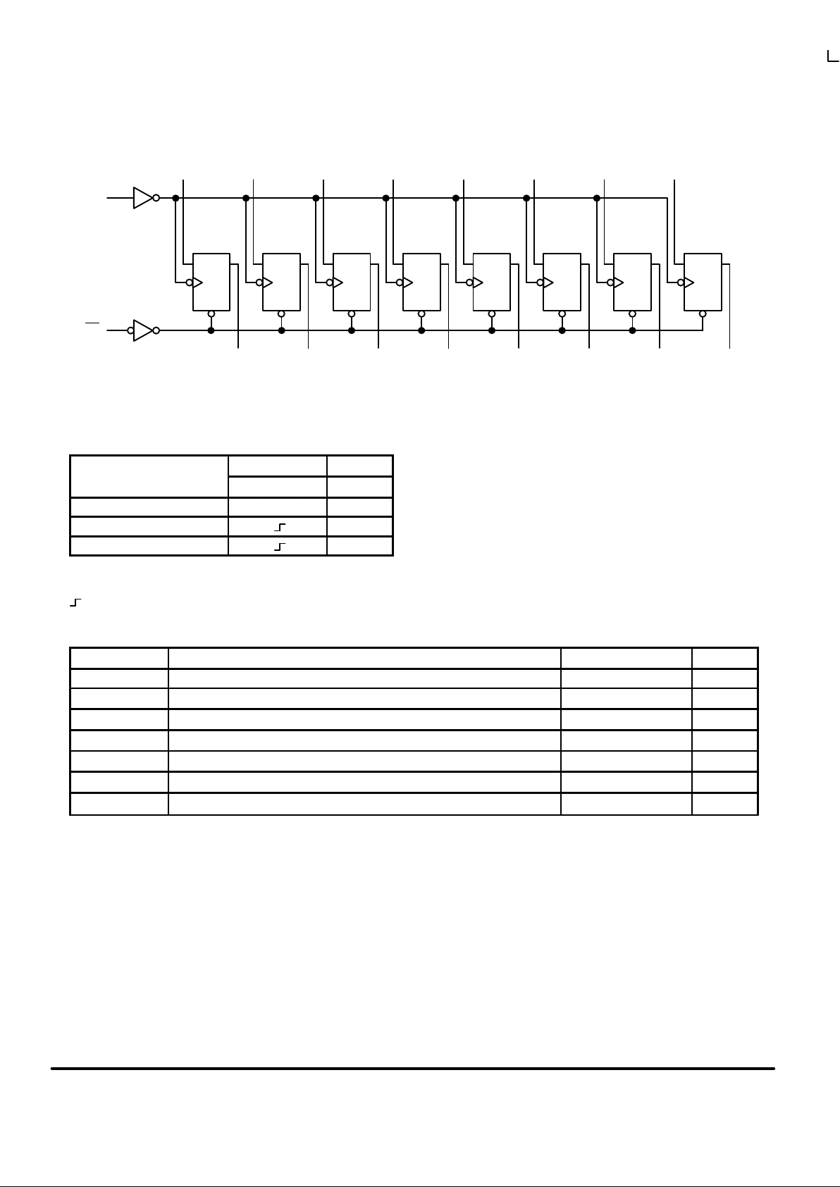
The MC74AC273/74ACT273 has eight edge-triggered D-type flip-flops with
individual D inputs and Q outputs. The common buffered Clock (CP) and Master
Reset (MR
) inputs load and reset (clear) all flip-flops simultaneously.
The register is fully edge-triggered. The state of each D input, one setup time
before the LOW-to-HIGH clock transition, is transferred to the corresponding flip-
flop’s Q output.
All outputs will be forced LOW independently of Clock or Data inputs by a LOW
voltage level on the MR
input. The device is useful for applications where the true
output only is required and the Clock and Master Reset are common to all storage
elements.
• Ideal Buffer for MOS Microprocessor or Memory
• Eight Edge-Triggered D Flip-Flops
• Buffered Common Clock
• Buffered, Asynchronous Master Reset
• See MC74AC377 for Clock Enable Version
• See MC74AC373 for Transparent Latch Version
• See MC74AC374 for 3-State Version
• Outputs Source/Sink 24 mA
• ′ACT273 Has TTL Compatible Inputs
1920 18 17 16 15 14
21 3 4 5 6 7
V
CC
13
8
12
9
11
10
Q
7
D
7
D
6
Q
6
Q
5
D
5
D
4
Q
4
CP
MR
Q
0
D
0
D
1
Q
1
Q
2
D
2
D
3
Q
3
GND
PIN NAMES
D
0
–D
7
Data Inputs
MR
Master Reset
CP Clock Pulse Input
Q
0
–Q
7
Data Outputs
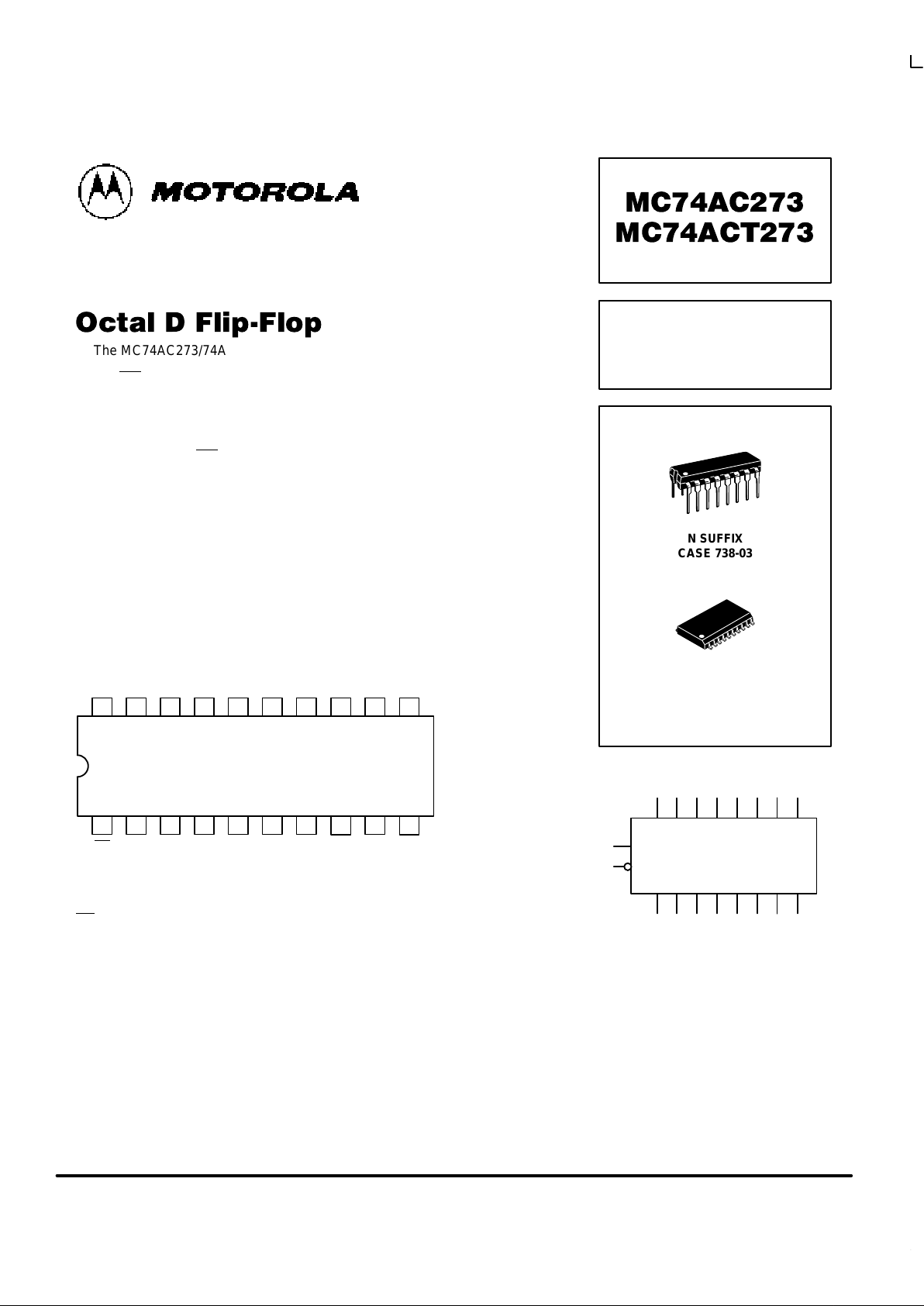
OCTAL D FLIP-FLOP
N SUFFIX
CASE 738-03
PLASTIC
DW SUFFIX
CASE 751D-04
PLASTIC
LOGIC SYMBOL
Q
0
Q
1
Q
2
Q
3
Q
4
Q
5
Q
6
Q
7
D
0
D
1
D
2
D
3
D
4
D
5
D
6
D
7
CP
MR
MC74AC273 MC74ACT273
5-2
FACT DATA
D
0
D
1
D
2
D
3
D
4
D
5
D
6
D
7
O
0
O
1
O
2
O
3
O
4
O
5
O
6
O
7
D Q
CP
R
D
D Q
CP
R
D
D Q
CP
R
D
D Q
CP
R
D
D Q
CP
R
D
D Q
CP
R
D
D Q
CP
R
D
D Q
CP
R
D
CP
MR
Please note that this diagram is provided only for the understanding of logic
operations and should not be used to estimate propagation delays.
LOGIC DIAGRAM
MODE SELECT-FUNCTION TABLE
Inputs Outputs
Operating Mode
MR CP D
n
Q
n
Reset (Clear) L X X L
Load ′1′ H H H
Load ′0′ H L L
H = HIGH Voltage Level
L = LOW Voltage Level
X = Immaterial
= LOW-to-HIGH Clock Transition
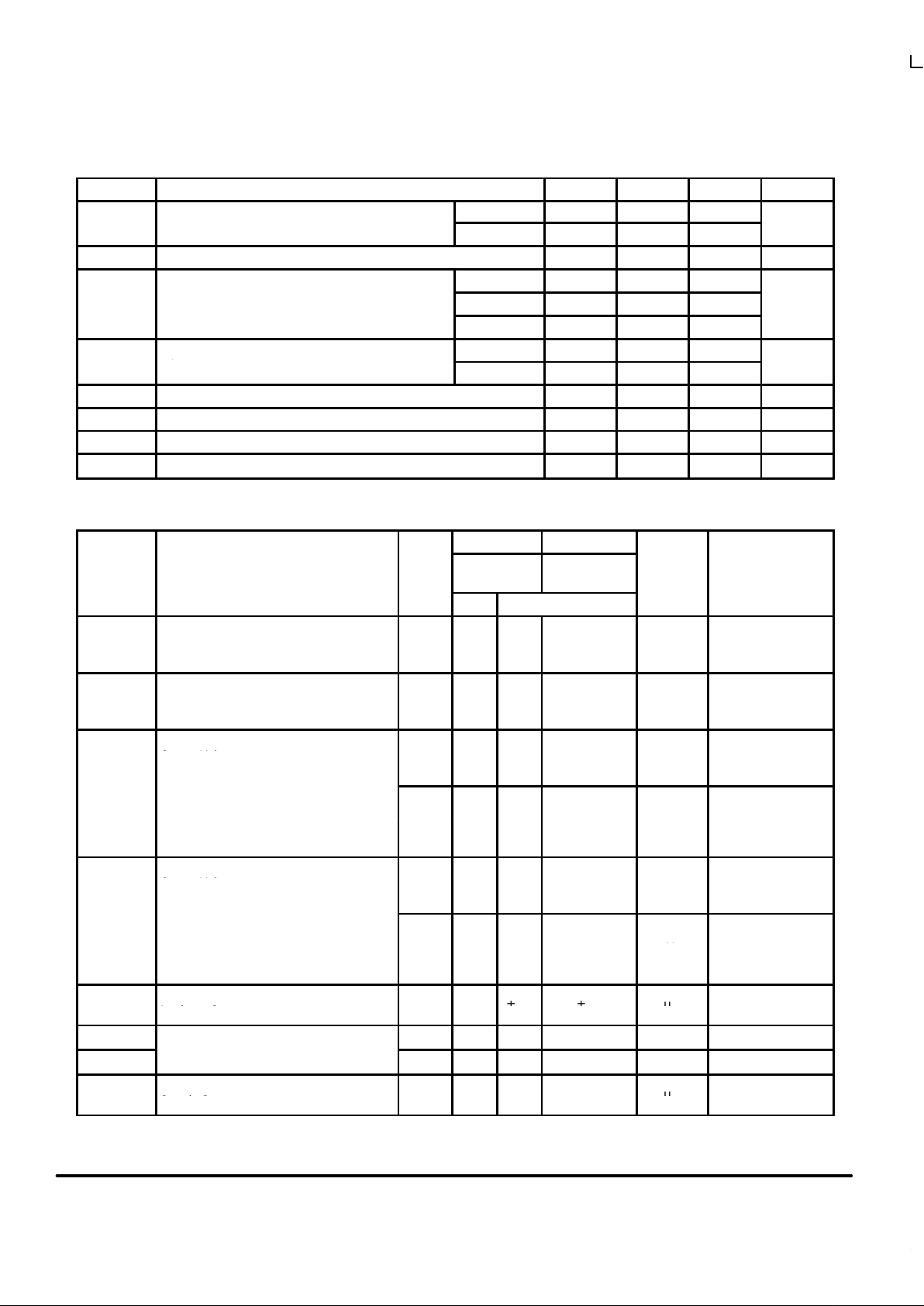
MAXIMUM RATINGS*
Symbol Parameter Value Unit
V
CC
DC Supply Voltage (Referenced to GND) –0.5 to +7.0 V
V
in
DC Input Voltage (Referenced to GND) –0.5 to V
CC
+0.5 V
V
out
DC Output Voltage (Referenced to GND) –0.5 to V
CC
+0.5 V
I
in
DC Input Current, per Pin ±20 mA
I
out
DC Output Sink/Source Current, per Pin ±50 mA
I
CC
DC V
CC
or GND Current per Output Pin ±50 mA
T
stg
Storage Temperature –65 to +150 °C
* Maximum Ratings are those values beyond which damage to the device may occur. Functional operation should be restricted to the Recommended
Operating Conditions.
MC74AC273 MC74ACT273
5-3
FACT DATA
RECOMMENDED OPERATING CONDITIONS
Symbol Parameter Min Typ Max Unit
′AC 2.0 5.0 6.0
V
CC
Supply Voltage
′ACT 4.5 5.0 5.5
V
V
in
, V
out
DC Input Voltage, Output Voltage (Ref. to GND) 0 V
CC
V
V
CC
@ 3.0 V 150
t
r
, t
f
Input Rise and Fall Time (Note 1)
′AC Devices except Schmitt Inputs
V
CC
@ 4.5 V 40 ns/V
r
, t
f
′AC Devices except Schmitt Inputs
V
CC
@ 5.5 V 25
Input Rise and Fall Time (Note 2)
V
CC
@ 4.5 V 10
t
r
, t
f
Input Rise and Fall Time (Note 2)
′ACT Devices except Schmitt Inputs
V
CC
@ 5.5 V 8.0
ns/V
T
J
Junction Temperature (PDIP) 140 °C
T
A
Operating Ambient Temperature Range –40 25 85 °C
I
OH
Output Current — High –24 mA
I
OL
Output Current — Low 24 mA
1. V
in
from 30% to 70% V
CC
; see individual Data Sheets for devices that differ from the typical input rise and fall times.
2. V
in
from 0.8 V to 2.0 V; see individual Data Sheets for devices that differ from the typical input rise and fall times.
DC CHARACTERISTICS
74AC 74AC
Symbol
Parameter
V
CC
(V)
T
A
= +25°C
T
A
=
–40°C to +85°C
Unit
Conditions
Typ Guaranteed Limits
V
IH
Minimum High Level
3.0 1.5 2.1 2.1 V
OUT
= 0.1 V
Input Voltage
4.5 2.25 3.15 3.15 V or V
CC
– 0.1 V
5.5 2.75 3.85 3.85
V
IL
Maximum Low Level
3.0 1.5 0.9 0.9 V
OUT
= 0.1 V
Input Voltage
4.5 2.25 1.35 1.35 V or V
CC
– 0.1 V
5.5 2.75 1.65 1.65
V
OH
Minimum High Level
3.0 2.99 2.9 2.9 I
OUT
= –50 µA
Output Voltage
4.5 4.49 4.4 4.4 V
5.5 5.49 5.4 5.4
*V
IN
= V
IL
or V
IH
3.0 2.56 2.46
–12 mA
4.5 3.86 3.76
V
I
OH
–24 mA
5.5 4.86 4.76 –24 mA
V
OL
Maximum Low Level
3.0 0.002 0.1 0.1 I
OUT
= 50 µA
Output Voltage
4.5 0.001 0.1 0.1 V
5.5 0.001 0.1 0.1
*V
IN
= V
IL
or V
IH
3.0 0.36 0.44
12 mA
4.5 0.36 0.44
V
I
OL
24 mA
5.5 0.36 0.44 24 mA
I
IN
Maximum Input
Leakage Current
5.5
±0.1
±1.0
µA
V
I
= V
CC
, GND
I
OLD
†Minimum Dynamic
5.5 75 mA V
OLD
= 1.65 V Max
I
OHD
Output Current
5.5 –75 mA V
OHD
= 3.85 V Min
I
CC
Maximum Quiescent
Supply Current
5.5
8.0
80
µA
V
IN
= V
CC
or GND
* All outputs loaded; thresholds on input associated with output under test.
†Maximum test duration 2.0 ms, one output loaded at a time.
Note: I
IN
and I
CC
@ 3.0 V are guaranteed to be less than or equal to the respective limit @ 5.5 V V
CC
.
 Loading...