


 Loading...
Motorola MC68L11FC0FU4, MC68L11FC0PU3, MC68L11FC0PU4, MC68L11F1CFN3, MC68L11F1CPU3 Datasheet
...MOTOROLA
SEMICONDUCTOR
TECHNICAL DATA
Order this document by MC68HC11FTS/D
MC68HC11F1
MC68HC11FC0
Technical Summary
8-Bit Microcontroller
1 Introduction
The MC68HC11F1 is a high-performance member of the M68HC11 family of microcontroller units (MCUs). High-speed expanded systems required the development of this chip with its extra input/output (I/O) ports, an increase in static RAM (one Kbyte), internal chip-select functions, and a non-multiplexed bus which reduces the need for external interface logic. The timer, serial I/O, and analog-to-digital (A/ D) converter enable functions similar to those found in the MC68HC11E9.
The MC68HC11FC0 is a low cost, high-speed derivative of the MC68HC11F1. It does not have EEPROM or an analog-to-digital converter. The MC68HC11FC0 can operate at bus speeds as high as six MHz.
This document provides a brief overview of the structure, features, control registers, packaging information and availability of the MC68HC11F1 and MC68HC11FC0. For detailed information on M68HC11 subsystems, programming and the instruction set, refer to the M68HC11 Reference Manual (M68HC11RM/AD).
1.1Features
•MC68HC11 CPU
•512 Bytes of On-Chip Electrically Erasable Programmable ROM (EEPROM) with Block Protect (MC68HC11F1 only)
•1024 Bytes of On-Chip RAM (All Saved During Standby)
•Enhanced 16-Bit Timer System
—3 Input Capture (IC) Functions
—4 Output Compare (OC) Functions
—4th IC or 5th OC (Software Selectable)
•On-Board Chip-Selects with Clock Stretching
•Real-Time Interrupt Circuit
•8-Bit Pulse Accumulator
•Synchronous Serial Peripheral Interface (SPI)
•Asynchronous Nonreturn to Zero (NRZ) Serial Communication Interface (SCI)
•Power saving STOP and WAIT Modes
•Eight-Channel 8-Bit A/D Converter (MC68HC11F1 only)
•Computer Operating Properly (COP) Watchdog System and Clock Monitor
•Bus Speeds of up to 6 MHz for the MC68HC11FC0 and up to 5 MHz for the MC68HC11F1
•68-Pin PLCC (MC68HC11F1 only), 64-Pin QFP (MC68HC11FC0 only), and 80-pin TQFP package options
This document contains information on a new product. Specifications and information herein are subject to change without notice.
M
© MOTOROLA INC., 1997

1.2 Ordering Information
The following devices all have 1024 bytes of RAM. In addition, the MC68HC11F1 devices have 512 bytes of EEPROM. None of the devices contain on-chip ROM.
Table 1 MC68HC11F1 Standard Device Ordering Information
Package |
Temperature |
Frequency |
MC Order Number |
|
|
|
|
|
|
|
0° to +70° |
5 MHz |
MC68HC11F1PU5 |
|
|
|
|
|
|
|
|
2 MHz |
MC68HC11F1CPU2 |
|
|
|
|
|
|
|
-40° to +85°C |
3 MHz |
MC68HC11F1CPU3 |
|
|
|
|
||
|
4 MHz |
MC68HC11F1CPU4 |
||
|
|
|||
80-Pin Thin Quad Flat Pack |
|
|
|
|
|
5 MHz |
MC68HC11F1CPU5 |
||
(TQFP) |
|
|
|
|
|
2 MHz |
MC68HC11F1VPU2 |
||
(14 mm X 14 mm, |
|
|||
– 40° to + 105° C |
|
|
||
3 MHz |
MC68HC11F1VPU3 |
|||
1.4 mm thick) |
||||
|
|
|
|
|
|
|
4 MHz |
MC68HC11F1VPU4 |
|
|
|
|
|
|
|
|
2 MHz |
MC68HC11F1MPU2 |
|
|
– 40° to + 125° C |
|
|
|
|
3 MHz |
MC68HC11F1MPU3 |
||
|
|
|
|
|
|
|
4 MHz |
MC68HC11F1MPU4 |
|
|
|
|
|
|
|
0° to +70° |
5 MHz |
MC68HC11F1FN5 |
|
|
|
|
|
|
|
|
2 MHz |
MC68HC11F1CFN2 |
|
|
|
|
|
|
|
– 40° to + 85° C |
3 MHz |
MC68HC11F1CFN3 |
|
|
|
|
||
|
4 MHz |
MC68HC11F1CFN4 |
||
|
|
|||
|
|
|
|
|
|
|
5 MHz |
MC68HC11F1CFN5 |
|
68-Pin PLCC |
|
|
|
|
|
2 MHz |
MC68HC11F1VFN2 |
||
|
– 40° to + 105° C |
|
|
|
|
3 MHz |
MC68HC11F1VFN3 |
||
|
|
|
|
|
|
|
4 MHz |
MC68HC11F1VFN4 |
|
|
|
|
|
|
|
|
2 MHz |
MC68HC11F1MFN2 |
|
|
– 40° to + 125° C |
|
|
|
|
3 MHz |
MC68HC11F1MFN3 |
||
|
|
|
|
|
|
|
4 MHz |
MC68HC11F1MFN4 |
|
|
|
|
|
Table 2 MC68HC11F1 Extended Voltage (3.0 to 5.5 V) Device Ordering Information
Package |
Temperature |
Frequency |
MC Order Number |
|
|
|
|
68-Pin Plastic Leaded Chip |
0° to +70°C |
3 MHz |
MC68L11F1FN3 |
Carrier (PLCC) |
–40° to +85°C |
3 MHz |
MC68L11F1CFN3 |
|
|
|
|
80-Pin Thin Quad Flat Pack |
0° to +70°C |
3 MHz |
MC68L11F1PU3 |
(TQFP) |
–40° to +85°C |
3 MHz |
MC68L11F1CPU3 |
|
|
|
|
MOTOROLA |
MC68HC11F1/FC0 |
2 |
MC68HC11FTS/D |

Table 3 MC68HC11FC0 Standard Device Ordering Information
Package |
Temperature |
Frequency |
MC Order Number |
|
|
|
|
|
|
64-Pin Quad Flat Pack |
–40° to +85°C |
4 MHz |
MC68HC11FC0CFU4 |
|
|
|
|||
5 MHz |
MC68HC11FC0CFU5 |
|||
(QFP) |
|
|||
|
|
|
||
0° to 70° C |
6 MHz |
MC68HC11FC0FU6 |
||
|
||||
|
|
|
|
|
80-Pin Thin Quad Flat Pack |
–40° to +85°C |
4 MHz |
MC68HC11FC0CPU4 |
|
|
|
|||
5 MHz |
MC68HC11FC0CPU5 |
|||
(TQFP) |
|
|||
|
|
|
||
0° to 70° C |
6 MHz |
MC68HC11FC0PU6 |
||
|
||||
|
|
|
|
Table 4 MC68HC11FC0 Extended Voltage (3.0 to 5.5 V) Device Ordering Information
Package |
Temperature |
Frequency |
MC Order Number |
|
|
|
|
|
|
64-Pin Quad Flat Pack |
|
3 MHz |
MC68L11FC0FU3 |
|
(QFP) |
–0° to +70°C |
4 MHz |
MC68L11FC0FU4 |
|
|
|
|
||
80-Pin Thin Quad Flat Pack |
3 MHz |
MC68L11FC0PU3 |
||
|
||||
(TQFP) |
|
4 MHz |
MC68L11FC0PU4 |
|
|
|
|
|
MC68HC11F1/FC0 |
MOTOROLA |
MC68HC11FTS/D |
3 |

|
TABLE OF CONTENTS |
|
Section |
|
Page |
1 |
Introduction |
1 |
1.1 |
Features ...................................................................................................................................... |
1 |
1.2 |
Ordering Information ................................................................................................................... |
2 |
1.3 |
Block Diagrams .......................................................................................................................... |
6 |
2 |
Pin Assignments and Signal Descriptions |
8 |
2.1 |
MC68HC11F1 Pin Assignments .................................................................................................. |
8 |
2.2 |
MC68HC11FC0 Pin Assignments ............................................................................................. |
10 |
2.3 |
Pin Descriptions ........................................................................................................................ |
12 |
3 |
Control Registers |
14 |
3.1 |
MC68HC11F1 Control Registers ............................................................................................... |
14 |
3.2 |
MC68HC11FC0 Control Registers ............................................................................................ |
16 |
4 |
Operating Modes and System Initialization |
18 |
4.1 |
Operating Modes ....................................................................................................................... |
18 |
4.2 |
Memory Maps ............................................................................................................................ |
19 |
4.3 |
System Initialization Registers .................................................................................................. |
20 |
5 |
Resets and Interrupts |
25 |
5.1 |
Interrupt Sources ....................................................................................................................... |
25 |
5.2 |
Reset and Interrupt Registers ................................................................................................... |
26 |
6 |
Electrically Erasable Programmable ROM |
29 |
6.1 |
EEPROM Operation .................................................................................................................. |
29 |
6.2 |
EEPROM Registers ................................................................................................................... |
29 |
6.3 |
EEPROM Programming and Erasure ........................................................................................ |
31 |
6.4 |
CONFIG Register Programming ............................................................................................... |
32 |
7 |
Parallel Input/Output |
33 |
7.1 |
Port A ........................................................................................................................................ |
33 |
7.2 |
Port B ........................................................................................................................................ |
33 |
7.3 |
Port C ........................................................................................................................................ |
33 |
7.4 |
Port D ........................................................................................................................................ |
33 |
7.5 |
Port E ........................................................................................................................................ |
33 |
7.6 |
Port F ......................................................................................................................................... |
33 |
7.7 |
Port G ........................................................................................................................................ |
34 |
7.8 |
Parallel I/O Registers ................................................................................................................ |
34 |
8 |
Chip-Selects |
38 |
8.1 |
Chip-Select Operation ............................................................................................................... |
38 |
8.2 |
Chip-Select Registers ................................................................................................................ |
38 |
9 |
Serial Communications Interface (SCI) |
42 |
9.1 |
SCI Block Diagrams .................................................................................................................. |
42 |
9.2 |
SCI Registers ............................................................................................................................ |
44 |
10 |
Serial Peripheral Interface |
49 |
10.1 |
SPI Block Diagram .................................................................................................................... |
49 |
10.2 |
SPI Registers ............................................................................................................................ |
50 |
11 |
Analog-to-Digital Converter |
53 |
11.1 |
Input Pins .................................................................................................................................. |
54 |
11.2 |
Conversion Sequence ............................................................................................................... |
54 |
11.3 |
A/D Registers ............................................................................................................................ |
55 |
12 |
Main Timer |
57 |
12.1 |
Timer Operation ........................................................................................................................ |
57 |
12.2 |
Timer Registers ......................................................................................................................... |
59 |
13 |
Pulse Accumulator |
64 |
13.1 |
Pulse Accumulator Block Diagram ............................................................................................ |
64 |
13.2 |
Pulse Accumulator Registers .................................................................................................... |
64 |
MOTOROLA |
MC68HC11F1/FC0 |
4 |
MC68HC11FTS/D |

REGISTER INDEX
Register |
|
Address |
Page |
ADCTL ................ |
A/D Control/Status ......................................................... |
$1030 .......................... |
55 |
BAUD .................. |
Baud Rate...................................................................... |
$102B .......................... |
44 |
BPROT................ |
Block Protect.................................................................. |
$1035 .......................... |
29 |
CFORC ............... |
Timer Force Compare.................................................... |
$100B .......................... |
59 |
CONFIG .............. |
EEPROM Mapping, COP, EEPROM Enables ............... |
$103F ............. |
24, 28, 30 |
COPRST ............. |
Arm/Reset COP Timer Circuitry..................................... |
$103A .......................... |
27 |
CSCTL ................ |
Chip-Select Control........................................................ |
$105D .......................... |
39 |
CSGADR............. |
General-Purpose Chip-Select Address Register ........... |
$105E ......................... |
40 |
CSGSIZ............... |
General-Purpose Chip-Select Size Register ................ |
$105F .......................... |
40 |
CSSTRH ............. |
Clock Stretching............................................................. |
$105C .......................... |
38 |
DDRA .................. |
Port A Data Register...................................................... |
$1001 .......................... |
34 |
DDRC.................. |
Data Direction Register for Port C ................................. |
$1007 .......................... |
35 |
DDRD.................. |
Data Direction Register for Port D ................................. |
$1009 .......................... |
36 |
DDRG.................. |
Data Direction Register for Port G ................................. |
$1003 .......................... |
35 |
HPRIO................. |
Highest Priority Interrupt and Miscellaneous ................ |
$103C ................... |
20, 27 |
INIT ..................... |
RAM and I/O Mapping ................................................... |
$103D ................... |
21, 22 |
OC1D .................. |
Output Compare 1 Data ................................................ |
$100D .......................... |
59 |
OC1M.................. |
Output Compare 1 Mask ............................................... |
$100C .......................... |
59 |
OPT2................... |
System Configuration Option Register 2 ....................... |
$1038 ............. |
22, 36, 52 |
OPTION .............. |
System Configuration Options ....................................... |
$1039 ............. |
23, 26, 56 |
PACNT ................ |
Pulse Accumulator Count .............................................. |
$1027 .......................... |
66 |
PACTL................. |
Pulse Accumulator Control ........................................... |
$1026 ................... |
63, 65 |
PORTA................ |
Port A Data .................................................................... |
$1000 .......................... |
34 |
PORTB................ |
Port B Data .................................................................... |
$1004 .......................... |
35 |
PORTC................ |
Port C Data .................................................................... |
$1006 .......................... |
35 |
PORTD................ |
Port D Data .................................................................... |
$1008 .......................... |
36 |
PORTE................ |
Port E Data .................................................................... |
$100A .......................... |
36 |
PORTF ................ |
Port F Data .................................................................... |
$1005 .......................... |
35 |
PORTG ............... |
Port G Data.................................................................... |
$1002 .......................... |
34 |
PPROG ............... |
EEPROM Programming Control .................................... |
$103B .......................... |
30 |
SCCR1 ................ |
SCI Control 1 ................................................................ |
$102C .......................... |
46 |
SCCR2 ................ |
SCI Control 2 ................................................................ |
$102D .......................... |
46 |
SCDR .................. |
Serial Communications Data Register........................... |
$102F .......................... |
48 |
SCSR .................. |
SCI Status...................................................................... |
$102E .......................... |
47 |
SPCR .................. |
Serial Peripheral Control ............................................... |
$1028 .......................... |
50 |
SPDR .................. |
SPI Data ....................................................................... |
$102A .......................... |
51 |
SPSR .................. |
Serial Peripheral Status ................................................. |
$1029 .......................... |
51 |
TCNT................... |
Timer Count .................................................................. |
$100E, $100F .............. |
59 |
TCTL1 ................. |
Timer Control 1 .............................................................. |
$1020 .......................... |
60 |
TCTL2 ................. |
Timer Control 2 .............................................................. |
$1021 .......................... |
61 |
TEST1 ................. |
Factory Test .................................................................. |
$103E .......................... |
24 |
TFLG1 ................. |
Timer Interrupt Flag 1 ................................................... |
$1023 .......................... |
61 |
TFLG2 ................. |
Timer Interrupt Flag 2 ................................................... |
$1025 ................... |
62, 65 |
TI4O5 .................. |
Timer Input Capture 4/Output Compare 5 .................... |
$101E, $101F .............. |
60 |
TIC1–TIC3........... |
Timer Input Capture ...................................................... |
$1010–$1015 .............. |
60 |
TMSK1 ................ |
Timer Interrupt Mask 1 .................................................. |
$1022 .......................... |
61 |
TMSK2 ................ |
Timer Interrupt Mask 2 .................................................. |
$1024 ................... |
62, 64 |
TOC1–TOC4 ....... |
Timer Output Compare ................................................. |
$1016–$101D .............. |
60 |
MC68HC11F1/FC0 |
MOTOROLA |
MC68HC11FTS/D |
5 |

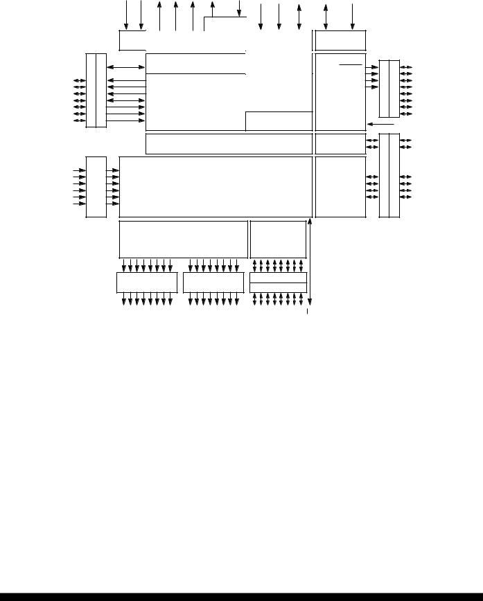
1.3 Block Diagrams
|
E |
|
|
|
|
|
|
|
MODA/ |
MODB/ |
VDD VSS |
4XOUT XTAL |
EXTAL |
IRQ |
|
XIRQ |
|
RESET |
LIR |
VSTBY |
PA7 

PA6 |
A |
PA5 |
PORT |
PA4 |
|
PA3 |
|
PA2 |
|
PA1 |
|
PA0 |
|
|
|
OSCILLATOR |
|
|
|
POWER |
CLOCK |
INTERRUPT |
MODE |
|
LOGIC |
LOGIC |
CONTROL |
|
|
|
|||
|
PAI/0C1 |
PULSE |
COP |
A/D |
|
ACCUMULATOR |
|||
|
CONVERTER |
|||
|
|
|
|
|
|
OC2/OC1 |
|
|
AN7 |
DDRA |
|
TIMER |
AN6 |
|
OC3/OC1 |
|
|||
|
AN5 |
|||
OC4/OC1 |
|
SYSTEM |
||
|
AN4 |
|||
|
IC4/OC5/OC1 |
|
AN3 |
|
|
IC3 |
|
|
|
|
|
|
AN2 |
|
|
IC2 |
|
|
|
|
|
|
AN1 |
|
|
IC1 |
|
PERIODIC INTERRUPT |
|
|
|
AN0 |
||
PORT E
VRH
VRL
PE7
PE6
PE5
PE4
PE3
PE2
PE1
PE0
512 BYTES EEPROM
1024 BYTES STATIC RAM
CPU
CORE
|
|
|
|
|
|
ADDRESS BUS |
|
|
|
|
|
|
|
DATA BUS |
|
|||
ADDR15 |
ADDR14 |
ADDR13 |
ADDR12 |
ADDR11 |
ADDR10 |
ADDR9 |
ADDR8 |
ADDR7 |
ADDR6 |
ADDR5 |
ADDR4 |
ADDR3 |
ADDR2 |
ADDR1 |
ADDR0 |
DATA7 |
DATA6 DATA5 DATA4 DATA3 DATA2 DATA1 DATA0 |
|
|
|
PORT B |
|
|
|
|
PORT F |
|
|
|
PORT C |
|
||||||
|
|
|
|
|
|
|
|
|
DDRC |
|
||||||||
|
|
|
|
|
|
|
|
|
|
|
|
|
|
|
|
|
|
|
PB7 |
PB6 |
PB5 |
PB4 |
PB3 |
PB2 |
PB1 |
PB0 |
PF0 |
PF1 |
PF2 |
PF3 |
PF4 |
PF5 |
PF6 |
PF7 |
PC0 |
PC1 PC2 PC3 PC4 PC5 PC6 PC7 |
R/W |
CSPROG |
|
|
PG7 |
|
CSGEN |
PORTG |
|
PG6 |
|
|
CSIO1 |
DDRG |
PG5 |
|
|
CSIO2 |
PG3 |
||
|
|
|
PG4 |
|
|
|
|
|
PG2 |
|
|
|
|
PG1 |
CHIP |
|
|
|
PG0 |
SELECTS |
|
|
|
|
SCI |
RxD |
|
|
PD0 |
TxD |
|
|
PD1 |
|
|
|
|
||
|
MOSI |
DDRD |
PORTD |
PD3 |
|
MISO |
|
|
PD2 |
|
SCK |
|
|
PD4 |
SPI |
SS |
|
|
PD5 |
|
|
|
|
|
Figure 1 MC68HC11F1 Block Diagram
MOTOROLA |
MC68HC11F1/FC0 |
6 |
MC68HC11FTS/D |
|
|
|
|
|
|
|
|
MODA / |
MODB / |
VDD VSS |
DS |
E 4XOUT XTAL EXTAL |
IRQ |
|
XIRQ |
|
RESET |
LIR |
VSTBY |
PA7 

PA6 |
A |
PA5 |
PORT |
PA4 |
|
PA3 |
|
PA2 |
|
PA1 |
|
PA0 |
|
|
|
OSCILLATOR |
|
|
POWER |
CLOCK |
INTERRUPT |
|
LOGIC |
LOGIC |
|
|
|
||
|
PAI/0C1 |
PULSE |
COP |
|
ACCUMULATOR |
||
DDRA |
OC2/OC1 |
|
TIMER |
OC3/OC1 |
|
||
OC4/OC1 |
|
SYSTEM |
|
|
IC4/OC5/OC1 |
|
|
|
IC3 |
|
|
|
IC2 |
|
|
|
IC1 |
|
PERIODIC INTERRUPT |
|
|
1024 BYTES STATIC RAM |
|
PE6 |
|
|
|
|
|
|
|
|
|
|
|
|
|
|
|
|
|
PE5 |
E |
|
|
|
|
|
|
|
|
|
|
CPU |
|
|
|
|
|
PE4 |
|
|
|
|
|
|
|
|
|
|
|
|
|
|
|
||
PORT |
|
|
|
|
|
|
|
|
|
|
|
|
|
|
|
||
PE3 |
|
|
|
|
|
|
|
|
|
|
CORE |
|
|
|
|
|
|
PE2 |
|
|
|
|
|
|
|
|
|
|
|
|
|
|
|
|
|
PE1 |
|
|
|
|
|
|
|
|
|
|
|
|
|
|
|
|
|
|
|
|
|
|
|
|
ADDRESS BUS |
|
|
|
|
|
DATA BUS |
|
|||
|
ADDR15 |
ADDR14 |
ADDR13 |
ADDR12 |
ADDR11 |
ADDR10 |
ADDR9 |
ADDR8 |
ADDR7 |
ADDR6 |
ADDR5 |
ADDR4 ADDR3 ADDR2 |
ADDR1 |
ADDR0 |
DATA7 |
DATA6 DATA5 DATA4 DATA3 DATA2 DATA1 DATA0 |
|
|
|
|
PORT B |
|
|
|
|
PORT F |
|
|
|
PORT C |
|
||||
|
|
|
|
|
|
|
|
|
|
DDRC |
|
||||||
|
|
|
|
|
|
|
|
|
|
|
|
|
|
|
|
|
|
|
PB7 |
PB6 |
PB5 |
PB4 |
PB3 |
PB2 |
PB1 |
PB0 |
PF0 |
PF1 |
PF2 |
PF3 PF4 PF5 |
PF6 |
PF7 |
PC0 |
PC1 PC2 PC3 PC4 PC5 PC6 PC7 |
R/W |
MODE
CONTROL
CSPROG |
|
|
PG7 |
|
CSGEN |
PORTG |
|
PG6 |
|
|
CSIO1 |
DDRG |
PG5 |
|
|
CSIO2 |
PG4 |
||
|
|
|
|
PG3 |
|
|
|
|
PG2 |
|
|
|
|
PG1 |
CHIP |
|
|
|
PG0 |
SELECTS |
|
|
WAIT |
|
SCI |
RxD |
|
|
PD0 |
TxD |
|
|
PD1 |
|
|
|
|
||
|
MOSI |
DDRD |
PORTD |
PD3 |
|
MISO |
|
|
PD2 |
|
SCK |
|
|
PD4 |
SPI |
SS |
|
|
PD5 |
|
|
|
|
|
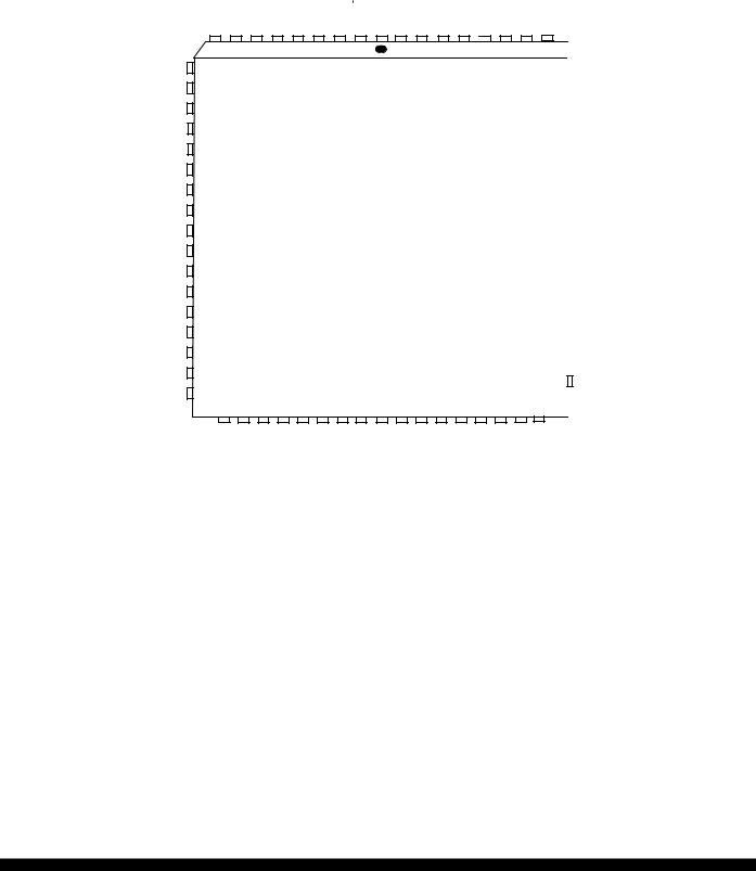
Figure 2 MC68HC11FC0 Block Diagram
MC68HC11F1/FC0 |
MOTOROLA |
MC68HC11FTS/D |
7 |
2 Pin Assignments and Signal Descriptions
2.1 MC68HC11F1 Pin Assignments
|
|
|
|
|
|
|
|
|
PC0/DATA0 |
|
|
|
|
|
|
MODA/LIR |
STBY |
|
|
|
|
PE7/AN7 |
PE3/AN3 |
|
PE6/AN6 |
|
|
|
|
|
|
|
|
|
|
|
|
|
|
|
|
|
|
|
|
|
|||||||
|
|
|
|
|
|
|
|
|
4XOUT |
XTAL |
EXTAL |
R/W |
E |
|
MODB/V |
|
V |
V |
V |
|
||||||
|
|
|
|
|
|
|
|
|
|
|
||||||||||||||||
|
|
|
|
|
|
|
|
|
|
|
|
|
|
|
|
|
|
|
|
SS |
RH |
RL |
|
|
|
|
|
|
|
|
|
|
|
|
|
9 |
8 |
7 |
6 |
5 |
4 |
3 |
2 |
|
|
|
|
||||||
|
|
|
|
|
|
|
|
|
|
|
|
67 |
|
65 |
|
|
||||||||||
|
|
|
|
|
|
|
|
|
|
|
|
|
|
|||||||||||||
|
|
|
|
|
|
|
|
|
|
|
|
|
|
|
||||||||||||
|
|
|
|
|
|
|
|
|
|
|
68 |
66 |
64 |
|||||||||||||
PC1/DATA1 |
10 |
|
|
|
|
|
|
|
|
|
1 |
|
|
|
|
|
|
|||||||||
PC2/DATA2 |
11 |
|
|
|
|
|
|
|
|
|
|
|
|
|
|
|
|
|
||||||||
PC3/DATA3 |
12 |
|
|
|
|
|
|
|
|
|
|
|
|
|
|
|
|
|
||||||||
PC4/DATA4 |
13 |
|
|
|
|
|
|
|
|
|
|
|
|
|
|
|
|
|
||||||||
PC5/DATA5 |
14 |
|
|
|
|
|
|
|
|
|
|
|
|
|
|
|
|
|
||||||||
PC6/DATA6 |
15 |
|
|
|
|
|
|
|
|
|
|
|
|
|
|
|
|
|
||||||||
PC7/DATA7 |
16 |
|
|
|
|
|
|
|
|
|
|
|
|
|
|
|
|
|
||||||||
|
|
|
|
|
|
|
|
|
17 |
|
|
|
|
|
|
|
|
|
|
|
|
|
|
|
|
|
|
|
RESET |
|
|
|
|
|
|
|
|
|
|
|
|
|
|
|
|
|
|||||||
|
|
|
|
|
|
|
|
18 |
|
|
|
|
|
|
|
MC68HC11F1 |
|
|
|
|
||||||
|
|
|
XIRQ |
|
|
|
|
|
|
|
|
|
|
|||||||||||||
|
|
|
|
|
|
|
19 |
|
|
|
|
|
|
|
|
|
|
|
|
|
|
|
|
|
||
|
|
|
|
IRQ |
|
|
|
|
|
|
|
|
|
|
|
|
|
|
|
|
|
|||||
|
|
|
20 |
|
|
|
|
|
|
|
|
|
|
|
|
|
|
|
|
|
||||||
PG7/CSPROG |
|
|
|
|
|
|
|
|
|
|
|
|
|
|
|
|
|
|||||||||
PG6/CSGEN |
21 |
|
|
|
|
|
|
|
|
|
|
|
|
|
|
|
|
|
||||||||
PG5/CSIO1 |
22 |
|
|
|
|
|
|
|
|
|
|
|
|
|
|
|
|
|
||||||||
PG4/CSIO2 |
23 |
|
|
|
|
|
|
|
|
|
|
|
|
|
|
|
|
|
||||||||
|
|
|
PG3 |
24 |
|
|
|
|
|
|
|
|
|
|
|
|
|
|
|
|
|
|||||
|
|
|
PG2 |
25 |
|
|
|
|
|
|
|
|
|
|
|
|
|
|
|
|
|
|||||
|
|
|
PG1 |
26 |
|
|
|
|
|
|
|
|
|
|
|
|
|
|
|
|
|
|||||
|
|
|
|
|
|
|
|
|
27 |
28 |
29 |
30 |
31 |
32 |
33 |
34 |
35 |
36 |
37 |
38 |
39 |
40 |
||||
|
|
|
|
|
|
|
|
|
PG0 |
PD0/RxD |
PD1/TxD |
PD2/MISO |
PD3/MOSI |
PD4/SCK |
|
|
PD5/SS |
DD |
|
PA7/PAI/OC1 |
PA6/OC2/OC1 |
PA5/OC3/OC1 |
PA4/OC4/OC1 |
PA3/OC5/IC4/OC1 |
PA2/IC1 |
|
|
|
|
|
|
|
|
|
|
|
|
|
|||||||||||||||
|
|
|
|
|
|
|
|
|
|
|
V |
|
||||||||||||||
63 PE2/AN2
PA1/IC2 41
62 PE5/AN5
PA0/IC3 42
61 PE1/AN1
PB7/ADDR15 43
60 |
|
PE4/AN4 |
|
||
59 |
|
PE0/AN0 |
|
||
58 |
|
PF0/ADDR0 |
|
||
57 |
|
PF1/ADDR1 |
|
||
56 |
|
PF2/ADDR2 |
|
||
55 |
|
PF3/ADDR3 |
|
||
54 |
|
PF4/ADDR4 |
|
||
53 |
|
PF5/ADDR5 |
|
||
52 |
|
PF6/ADDR6 |
|
||
51 |
|
PF7/ADDR7 |
|
||
50 |
|
PB0/ADDR8 |
|
||
49 |
|
PB1/ADDR9 |
|
||
48 |
|
PB2/ADDR10 |
|
||
47 |
|
PB3/ADDR11 |
|
||
46 |
|
PB4/ADDR12 |
|
||
45 |
|
PB5/ADDR13 |
44 |
|
PB6/ADDR14 |
|
||
|
|
|
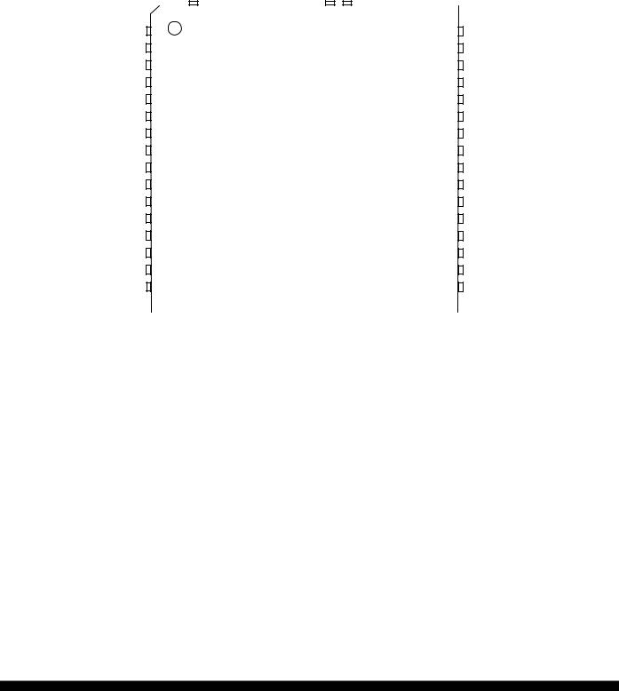
Figure 3 MC68HC11F1 68-Pin PLCC Pin Assignments
MOTOROLA |
MC68HC11F1/FC0 |
8 |
MC68HC11FTS/D |

|
|
|
|
|
|
NC |
|
|
NC |
|
|
PB7/ADDR15 |
|
|
PA0/IC3 |
|
|
PA1/IC2 |
|
|
PA2/IC1 |
|
|
PA3/OC5/IC4/OC1 |
|
|
PA4/OC4/OC1 |
|
|
PA5/OC3/OC1 |
PA6/OC2/OC1 |
|
PA7/PAI/OC1 |
|
V |
|
PD5/SS |
|
|
PD4/SCK |
|
PD3/MOSI |
|
|
PD2/MISO |
|
|
PD1/TXD |
|
|
PD0/RXD |
|
|
PG0 |
|
|
NC |
|
|
|
|
|
|
|
|||||||||||||||||||||||||||||||
|
|
|
|
|
|
|
|
|
|
|
|
|
|
|
|
|
|
|
|
|
|||||||||||||||||||||||||||||||||||||||||||||||||||||||||||||||||||||||||||
|
|
|
|
|
|
|
|
|
|
|
|
|
|
|
|
|
|
|
|
|
|||||||||||||||||||||||||||||||||||||||||||||||||||||||||||||||||||||||||||
|
|
|
|
|
|
|
|
|
|
|
|
|
|
|
|
|
|
|
|
|
|
|
|
|
|
|
|
|
|
|
|
|
|
|
|
|
|
|
|
|
|
|
|
|
|
|
|
|
|
|
DD |
|
|
|
|
|
|
|
|
|
|
|
|
|
|
|
|
|
|
|
|
|
|
|
|
|
|
|
|
|
|
|
|
|
|
|
|
|
|
|
|
|
|||
|
|
|
|
|
|
|
|
|
|
|
|
|
|
|
|
|
|
|
|
|
|
|
|
|
|
|
|
|
|
|
|
|
|
|
|
|
|
|
|
|
|
|
|
|
|
|
|
|
|
|
|
|
|
|
|
|
|
|
|
|
|
|
|
|
|
|
|
|
|
|
|
|
|
|
|
|
|
|
|
|
|
|
|
|
|
|
|
|
|
|
|
|
|
|
|
|
|
|
|
80 |
79 |
78 |
77 |
76 |
75 |
74 |
73 |
72 |
|
71 |
|
70 |
|
69 |
|
|
|
68 |
67 |
|
|
66 |
65 |
64 |
63 |
62 |
61 |
|
|
|
|
|
|
|
|
|
|||||||||||||||||||||||||||||||||||||||||||||||||||||||
NC |
|
|
|
1 |
|
|
|
|
|
|
|
|
|
|
|
|
|
|
|
|
|
|
|
|
|
|
|
|
|
|
|
|
|
|
|
|
|
|
|
|
|
|
|
|
|
|
|
|
|
|
|
|
|
|
|
|
|
|
|
|
|
|
|
|
|
|
|
|
|
|
|
|
|
|
|
|
|
|
|
|
|
60 |
|
|
NC |
||||||||||
|
|
|
|
|
|
|
|
|
|
|
|
|
|
|
|
|
|
|
|
|
|
|
|
|
|
|
|
|
|
|
|
|
|
|
|
|
|
|
|
|
|
|
|
|
|
|
|
|
|
|
|
|
|
|
|
|
|
|
|
|
|
|
|
|
|
|
|
|
|
|
|
|
|
|
|
|
|
|
|
|
|
||||||||||||||
NC |
|
|
|
2 |
|
|
|
|
|
|
|
|
|
|
|
|
|
|
|
|
|
|
|
|
|
|
|
|
|
|
|
|
|
|
|
|
|
|
|
|
|
|
|
|
|
|
|
|
|
|
|
|
|
|
|
|
|
|
|
|
|
|
|
|
|
|
|
|
|
|
|
|
|
|
|
|
|
|
|
|
|
59 |
|
|
PG1 |
||||||||||
|
|
|
|
|
|
|
|
|
|
|
|
|
|
|
|
|
|
|
|
|
|
|
|
|
|
|
|
|
|
|
|
|
|
|
|
|
|
|
|
|
|
|
|
|
|
|
|
|
|
|
|
|
|
|
|
|
|
|
|
|
|
|
|
|
|
|
|
|
|
|
|
|
|
|
|
|
|
|
|
|
|
||||||||||||||
PB6/ADDR14 |
|
|
|
3 |
|
|
|
|
|
|
|
|
|
|
|
|
|
|
|
|
|
|
|
|
|
|
|
|
|
|
|
|
|
|
|
|
|
|
|
|
|
|
|
|
|
|
|
|
|
|
|
|
|
|
|
|
|
|
|
|
|
|
|
|
|
|
|
|
|
|
|
|
|
|
|
|
|
|
|
|
|
58 |
|
|
PG2 |
||||||||||
|
|
|
|
|
|
|
|
|
|
|
|
|
|
|
|
|
|
|
|
|
|
|
|
|
|
|
|
|
|
|
|
|
|
|
|
|
|
|
|
|
|
|
|
|
|
|
|
|
|
|
|
|
|
|
|
|
|
|
|
|
|
|
|
|
|
|
|
|
|
|
|
|
|
|
|
|
|
|
|
|
|
||||||||||||||
PB5/ADDR13 |
|
|
|
4 |
|
|
|
|
|
|
|
|
|
|
|
|
|
|
|
|
|
|
|
|
|
|
|
|
|
|
|
|
|
|
|
|
|
|
|
|
|
|
|
|
|
|
|
|
|
|
|
|
|
|
|
|
|
|
|
|
|
|
|
|
|
|
|
|
|
|
|
|
|
|
|
|
|
|
|
|
|
57 |
|
|
PG3 |
||||||||||
|
|
|
|
|
|
|
|
|
|
|
|
|
|
|
|
|
|
|
|
|
|
|
|
|
|
|
|
|
|
|
|
|
|
|
|
|
|
|
|
|
|
|
|
|
|
|
|
|
|
|
|
|
|
|
|
|
|
|
|
|
|
|
|
|
|
|
|
|
|
|
|
|
|
|
|
|
|
|
|
|
|
||||||||||||||
PB4/ADDR12 |
|
|
|
5 |
|
|
|
|
|
|
|
|
|
|
|
|
|
|
|
|
|
|
|
|
|
|
|
|
|
|
|
|
|
|
|
|
|
|
|
|
|
|
|
|
|
|
|
|
|
|
|
|
|
|
|
|
|
|
|
|
|
|
|
|
|
|
|
|
|
|
|
|
|
|
|
|
|
|
|
|
|
56 |
|
|
PG4/CSIO2 |
||||||||||
|
|
|
|
|
|
|
|
|
|
|
|
|
|
|
|
|
|
|
|
|
|
|
|
|
|
|
|
|
|
|
|
|
|
|
|
|
|
|
|
|
|
|
|
|
|
|
|
|
|
|
|
|
|
|
|
|
|
|
|
|
|
|
|
|
|
|
|
|
|
|
|
|
|
|
|
|
|
|
|
|
|
||||||||||||||
PB3/ADDR11 |
|
|
6 |
|
|
|
|
|
|
|
|
|
|
|
|
|
|
|
|
|
|
|
|
|
|
|
|
|
|
|
|
|
|
|
|
|
|
|
|
|
|
|
|
|
|
|
|
|
|
|
|
|
|
|
|
|
|
|
|
|
|
|
|
|
|
|
|
|
|
|
|
|
|
|
|
|
|
|
|
|
55 |
|
|
PG5/CSIO1 |
|||||||||||
|
|
|
|
|
|
|
|
|
|
|
|
|
|
|
|
|
|
|
|
|
|
|
|
|
|
|
|
|
|
|
|
|
|
|
|
|
|
|
|
|
|
|
|
|
|
|
|
|
|
|
|
|
|
|
|
|
|
|
|
|
|
|
|
|
|
|
|
|
|
|
|
|
|
|
|
|
|
|
|
|
|||||||||||||||
PB2/ADDR10 |
|
|
7 |
|
|
|
|
|
|
|
|
|
|
|
|
|
|
|
|
|
|
|
|
|
|
|
|
|
|
|
|
|
|
|
|
|
|
|
|
|
|
|
|
|
|
|
|
|
|
|
|
|
|
|
|
|
|
|
|
|
|
|
|
|
|
|
|
|
|
|
|
|
|
|
|
|
|
|
|
|
54 |
|
|
PG6/CSGEN |
|||||||||||
|
|
|
|
|
|
|
|
|
|
|
|
|
|
|
|
|
|
|
|
|
|
|
|
|
|
|
|
|
|
|
|
|
|
|
|
|
|
|
|
|
|
|
|
|
|
|
|
|
|
|
|
|
|
|
|
|
|
|
|
|
|
|
|
|
|
|
|
|
|
|
|
|
|
|
|
|
|
|
|
|
|||||||||||||||
PB1/ADDR9 |
8 |
|
|
|
|
|
|
|
|
|
|
|
|
|
|
|
|
|
|
|
|
|
|
|
|
|
|
|
|
|
|
|
|
|
|
|
|
|
|
|
|
|
|
|
|
|
|
|
|
|
|
|
|
|
|
|
|
|
|
|
|
|
|
|
|
|
|
|
|
|
|
|
|
|
|
|
|
|
53 |
|
|
|
|
|
|
|
|||||||||
|
|
|
|
|
|
|
|
|
|
|
|
|
|
|
|
|
|
|
|
|
|
|
|
|
|
|
|
|
|
|
|
|
|
|
|
|
|
|
|
|
|
|
|
|
|
|
|
|
|
|
|
|
|
|
|
|
|
|
|
|
|
|
|
|
|
|
|
|
|
|
|
|
|
|
|
|
|
PG7/CSPROG |
|||||||||||||||||
PB0/ADDR8 |
9 |
|
|
|
|
|
|
|
|
|
|
|
|
|
|
|
|
|
|
|
|
|
|
|
|
|
|
|
|
|
|
|
|
|
|
|
|
|
|
|
|
|
|
|
|
|
|
|
|
|
|
|
|
|
|
|
|
|
|
|
|
|
|
|
|
|
|
|
|
|
|
|
|
|
|
|
|
|
52 |
|
|
|
|
|
|
|
|||||||||
|
|
|
|
|
|
|
|
|
|
|
|
|
|
|
|
|
|
|
|
|
|
|
|
|
|
|
|
|
|
|
|
|
|
|
|
|
|
|
|
|
|
|
|
|
|
|
|
|
|
|
|
|
|
|
|
|
|
|
|
|
|
|
|
|
|
|
|
|
|
|
|
|
|
|
|
|
|
|
IRQ |
|
|
|
|
||||||||||||
PF7/ADDR7 |
|
|
|
10 |
|
|
|
|
|
|
|
|
|
|
|
|
|
|
|
|
|
|
|
|
|
|
|
|
|
|
|
|
|
|
|
|
|
|
|
|
|
|
|
|
|
|
|
|
|
|
|
|
|
|
|
|
|
|
|
|
|
|
|
|
|
|
|
|
|
|
|
|
|
|
|
|
|
|
|
|
|
51 |
|
|
|
|
|
|
|
||||||
|
|
|
|
|
|
|
|
|
|
|
|
|
|
|
|
|
|
|
|
|
|
|
|
|
|
|
|
|
|
|
|
|
|
MC68HC11F1 |
|
|
|
|
|
|
|
|
|
|
|
|
|
|
|
|
|
|
|
|
|
|
|
|
|
|
|
|
|
|
XIRQ |
|
|
||||||||||||||||||||||||||||
PF6/ADDR6 |
|
|
|
11 |
|
|
|
|
|
|
|
|
|
|
|
|
|
|
|
|
|
|
|
|
|
|
|
|
|
|
|
|
|
|
|
|
|
|
|
|
|
|
|
|
|
|
|
|
|
|
|
|
|
|
|
|
|
|
|
|
|
|
|
50 |
|
|
|
|
|
|
|
||||||||||||||||||||||||
|
|
|
|
|
|
|
|
|
|
|
|
|
|
|
|
|
|
|
|
|
|
|
|
|
|
|
|
|
|
|
|
|
|
|
|
|
|
|
|
|
|
|
|
|
|
|
|
|
|
|
|
|
|
|
|
|
|
|
|
|
|
|
|
|
|
|
|
|
|
|
|
|
|
|
|
|
|
|
|
|
|
RESET |
|
||||||||||||
PF5/ADDR5 |
|
|
|
12 |
|
|
|
|
|
|
|
|
|
|
|
|
|
|
|
|
|
|
|
|
|
|
|
|
|
|
|
|
|
|
|
|
|
|
|
|
|
|
|
|
|
|
|
|
|
|
|
|
|
|
|
|
|
|
|
|
|
|
|
|
|
|
|
|
|
|
|
|
|
|
|
|
|
|
|
|
|
49 |
|
|
PC7/DATA7 |
||||||||||
|
|
|
|
|
|
|
|
|
|
|
|
|
|
|
|
|
|
|
|
|
|
|
|
|
|
|
|
|
|
|
|
|
|
|
|
|
|
|
|
|
|
|
|
|
|
|
|
|
|
|
|
|
|
|
|
|
|
|
|
|
|
|
|
|
|
|
|
|
|
|
|
|
|
|
|
|
|
|
|
|
|
||||||||||||||
PF4/ADDR4 |
|
|
|
13 |
|
|
|
|
|
|
|
|
|
|
|
|
|
|
|
|
|
|
|
|
|
|
|
|
|
|
|
|
|
|
|
|
|
|
|
|
|
|
|
|
|
|
|
|
|
|
|
|
|
|
|
|
|
|
|
|
|
|
|
|
|
|
|
|
|
|
|
|
|
|
|
|
|
|
|
|
|
48 |
|
|
PC6/DATA6 |
||||||||||
|
|
|
|
|
|
|
|
|
|
|
|
|
|
|
|
|
|
|
|
|
|
|
|
|
|
|
|
|
|
|
|
|
|
|
|
|
|
|
|
|
|
|
|
|
|
|
|
|
|
|
|
|
|
|
|
|
|
|
|
|
|
|
|
|
|
|
|
|
|
|
|
|
|
|
|
|
|
|
|
|
|
||||||||||||||
PF3/ADDR3 |
|
|
|
14 |
|
|
|
|
|
|
|
|
|
|
|
|
|
|
|
|
|
|
|
|
|
|
|
|
|
|
|
|
|
|
|
|
|
|
|
|
|
|
|
|
|
|
|
|
|
|
|
|
|
|
|
|
|
|
|
|
|
|
|
|
|
|
|
|
|
|
|
|
|
|
|
|
|
|
|
|
|
47 |
|
|
PC5/DATA5 |
||||||||||
|
|
|
|
|
|
|
|
|
|
|
|
|
|
|
|
|
|
|
|
|
|
|
|
|
|
|
|
|
|
|
|
|
|
|
|
|
|
|
|
|
|
|
|
|
|
|
|
|
|
|
|
|
|
|
|
|
|
|
|
|
|
|
|
|
|
|
|
|
|
|
|
|
|
|
|
|
|
|
|
|
|
||||||||||||||
PF2/ADDR2 |
|
|
|
15 |
|
|
|
|
|
|
|
|
|
|
|
|
|
|
|
|
|
|
|
|
|
|
|
|
|
|
|
|
|
|
|
|
|
|
|
|
|
|
|
|
|
|
|
|
|
|
|
|
|
|
|
|
|
|
|
|
|
|
|
|
|
|
|
|
|
|
|
|
|
|
|
|
|
|
|
|
|
46 |
|
|
PC4/DATA4 |
||||||||||
|
|
|
|
|
|
|
|
|
|
|
|
|
|
|
|
|
|
|
|
|
|
|
|
|
|
|
|
|
|
|
|
|
|
|
|
|
|
|
|
|
|
|
|
|
|
|
|
|
|
|
|
|
|
|
|
|
|
|
|
|
|
|
|
|
|
|
|
|
|
|
|
|
|
|
|
|
|
|
|
|
|
||||||||||||||
PF1/ADDR1 |
|
|
|
16 |
|
|
|
|
|
|
|
|
|
|
|
|
|
|
|
|
|
|
|
|
|
|
|
|
|
|
|
|
|
|
|
|
|
|
|
|
|
|
|
|
|
|
|
|
|
|
|
|
|
|
|
|
|
|
|
|
|
|
|
|
|
|
|
|
|
|
|
|
|
|
|
|
|
|
|
|
|
45 |
|
|
PC3/DATA3 |
||||||||||
|
|
|
|
|
|
|
|
|
|
|
|
|
|
|
|
|
|
|
|
|
|
|
|
|
|
|
|
|
|
|
|
|
|
|
|
|
|
|
|
|
|
|
|
|
|
|
|
|
|
|
|
|
|
|
|
|
|
|
|
|
|
|
|
|
|
|
|
|
|
|
|
|
|
|
|
|
|
|
|
|
|
||||||||||||||
PF0/ADDR0 |
17 |
|
|
|
|
|
|
|
|
|
|
|
|
|
|
|
|
|
|
|
|
|
|
|
|
|
|
|
|
|
|
|
|
|
|
|
|
|
|
|
|
|
|
|
|
|
|
|
|
|
|
|
|
|
|
|
|
|
|
|
|
|
|
|
|
|
|
|
|
|
|
|
|
|
|
|
|
|
44 |
|
|
PC2/DATA2 |
|||||||||||||
|
|
|
|
|
|
|
|
|
|
|
|
|
|
|
|
|
|
|
|
|
|
|
|
|
|
|
|
|
|
|
|
|
|
|
|
|
|
|
|
|
|
|
|
|
|
|
|
|
|
|
|
|
|
|
|
|
|
|
|
|
|
|
|
|
|
|
|
|
|
|
|
|
|
|
|
|
|
|
|||||||||||||||||
PE0/AN0 |
|
18 |
|
|
|
|
|
|
|
|
|
|
|
|
|
|
|
|
|
|
|
|
|
|
|
|
|
|
|
|
|
|
|
|
|
|
|
|
|
|
|
|
|
|
|
|
|
|
|
|
|
|
|
|
|
|
|
|
|
|
|
|
|
|
|
|
|
|
|
|
|
|
|
|
|
|
|
|
|
43 |
|
|
PC1/DATA1 |
||||||||||||
|
|
|
|
|
|
|
|
|
|
|
|
|
|
|
|
|
|
|
|
|
|
|
|
|
|
|
|
|
|
|
|
|
|
|
|
|
|
|
|
|
|
|
|
|
|
|
|
|
|
|
|
|
|
|
|
|
|
|
|
|
|
|
|
|
|
|
|
|
|
|
|
|
|
|
|
|
|
|
|
||||||||||||||||
PE4/AN4 |
|
19 |
|
|
|
|
|
|
|
|
|
|
|
|
|
|
|
|
|
|
|
|
|
|
|
|
|
|
|
|
|
|
|
|
|
|
|
|
|
|
|
|
|
|
|
|
|
|
|
|
|
|
|
|
|
|
|
|
|
|
|
|
|
|
|
|
|
|
|
|
|
|
|
|
|
|
|
|
|
42 |
|
|
NC |
||||||||||||
|
|
|
|
|
|
|
|
|
|
|
|
|
|
|
|
|
|
|
|
|
|
|
|
|
|
|
|
|
|
|
|
|
|
|
|
|
|
|
|
|
|
|
|
|
|
|
|
|
|
|
|
|
|
|
|
|
|
|
|
|
|
|
|
|
|
|
|
|
|
|
|
|
|
|
|
|
|
|
|
||||||||||||||||
NC |
|
|
|
20 |
|
|
|
|
|
|
|
|
|
|
|
|
|
|
|
|
|
|
|
|
|
|
|
|
|
|
|
|
|
|
|
|
|
|
|
|
|
|
|
|
|
|
|
|
|
|
|
|
|
|
|
|
|
|
|
|
|
|
|
|
|
|
|
|
|
|
|
|
|
|
|
|
|
|
|
|
|
41 |
|
|
NC |
||||||||||
|
|
|
|
|
|
|
|
|
|
|
|
|
|
|
|
|
|
|
|
|
|
|
|
|
|
|
|
|
|
|
|
|
|
|
|
|
|
|
|
|
|
|
|
|
|
|
|
|
|
|
|
|
|
|
|
|
|
|
|
|
|
|
|
|
|
|
|
|
|
|
|
|
|
|
|
|
|
|
|
|
|
||||||||||||||
|
|
|
|
21 |
22 |
23 |
24 |
25 |
26 |
27 |
28 |
29 |
|
30 |
|
31 |
|
32 |
|
|
|
33 |
34 |
|
|
35 |
36 |
37 |
38 |
39 |
40 |
|
|
|
|
|
|
|
|
|
|||||||||||||||||||||||||||||||||||||||||||||||||||||||
|
|
|
|
|
|
|
|
|
|
|
|
|
|
|
|
|
|
|
|
|
|||||||||||||||||||||||||||||||||||||||||||||||||||||||||||||||||||||||||||
|
|
|
|
|
|
|
|
|
|
|
|
|
|
|
|
|
|
|
|
|
|
|
|
|
|
|
|
|
|
|
|
|
|
|
|
|
|
|
|
|
|
|
|
|
|
|
|
|
|
|
|
|
|
|
|
|
|
|
|
|
|
|
|
|
|
|
|
|
|
|
|
|
|
|
|
|
|
|
|
|
|
|
|
|
|
|
|
|
|
|
|
|
|
|
|
|
|
|
|
|
|
NC |
|
|
NC |
|
|
PE1/AN1 |
|
|
PE5/AN5 |
|
|
PE2AN2 |
|
|
PE6/AN6 |
|
|
PE3/AN3 |
|
|
PE7/AN7 |
|
|
|
RL |
|
|
RH |
|
|
SS |
|
|
STBY |
|
|
MODA/LIR |
|
|
E |
|
R/W |
|
|
EXTAL |
|
|
XTAL |
|
NC |
|
|
4XOUT |
|
|
PC0/DATA0 |
|
|
|
|
|
|
|
||||||||||||||||||||||||||
|
|
|
|
|
|
|
|
|
|
|
|
|
|
|
|
|
|
|
|
|
|
|
|
|
|
|
|
|
|
|
|
|
|
|
|
|
|
|
|
|
|
|
|
|
|
|
|||||||||||||||||||||||||||||||||||||||||||||||||
|
|
|
|
|
|
|
|
|
|
|
|
|
|
|
|
|
|
|
|
|
|
|
|
|
|
|
|
|
|
|
|
|
|
|
|
|
|
|
|
|
|||||||||||||||||||||||||||||||||||||||||||||||||||||||
|
|
|
|
|
|
|
|
|
|
|
|
|
|
|
|
|
|
|
|
|
|
V |
|
V |
|
V |
|
|
|
|
|
|
|
|
|
|
|
|
|
|
|
|
|
|
|
|
|
||||||||||||||||||||||||||||||||||||||||||||||||
|
|
|
|
|
|
|
|
|
|
|
|
|
|
|
|
|
|
|
|
|
|
|
|
|
MODB/V |
|
|
|
|
|
|
|
|
|
|
|
|
|
|
|
|
|
|
|
|
||||||||||||||||||||||||||||||||||||||||||||||||||
Figure 4 Pin Assignments for the MC68HC11F1 80-Pin QFP
MC68HC11F1/FC0 |
MOTOROLA |
MC68HC11FTS/D |
9 |
2.2 MC68HC11FC0 Pin Assignments
|
|
|
PB7/ADDR15 |
|
|
PA0/IC3 |
PA1/IC2 |
|
|
PA2/IC1 |
PA3/IC4/OC5/OC1 |
|
|
PA4/OC4/OC1 |
|
|
|
PA5/OC3/OC1 |
|
|
PA6/OC2/OC1 |
|
|
PA7/PAI/OC1 |
|
V |
|
PD5/SS |
|
PD4/SCK |
PD3/MOSI |
|
PD2/MISO |
PD1/TxD |
|
PD0/RxD |
|
|
|
|
|
|||||||||||||||||||||||||||||||||||
|
|
|
|
|
|
|
|
|
||||||||||||||||||||||||||||||||||||||||||||||||||||||||||||||||||||
|
|
|
|
|
|
|
|
|
||||||||||||||||||||||||||||||||||||||||||||||||||||||||||||||||||||
|
|
|
|
|
|
|
|
|
|
|
|
|
|
|
|
|
|
|
|
|
|
|
|
|
|
|
|
|
|
|
|
|
|
|
|
|
|
|
|
|
|
DD |
|
|
|
|
|
|
|
|
|
|
|
|
|
|
|
|
|
|
|
|
|
|
|
|
|
|
|
|
|
|
|
|||
|
|
|
|
|
|
|
|
|
|
|
|
|
|
|
|
|
|
|
|
|
|
|
|
|
|
|
|
|
|
|
|
|
|
|
|
|
|
|
|
|
|
|
|
|
|
|
|
|
|
|
|
|
|
|
|
|
|
|
|
|
|
|
|
|
|
|
|
|
|
|
|
|
|
|
|
|
|
64 |
63 |
|
|
62 |
61 |
|
|
60 |
59 |
58 |
|
|
57 |
56 |
|
55 |
|
|
|
54 |
|
53 |
|
|
52 |
|
|
51 |
|
|
50 |
49 |
|
|
|
|
|
|
|
|
|||||||||||||||||||||||||||||||||||
PB6/ADDR14 |
1 |
|
|
|
|
|
|
|
|
|
|
|
|
|
|
|
|
|
|
|
|
|
|
|
|
|
|
|
|
|
|
|
|
|
|
|
|
|
|
|
|
|
|
|
|
|
|
|
|
|
|
|
|
|
|
|
|
|
|
|
|
|
|
48 |
|
PG2 |
||||||||||
PB5/ADDR13 |
2 |
|
|
|
|
|
|
|
|
|
|
|
|
|
|
|
|
|
|
|
|
|
|
|
|
|
|
|
|
|
|
|
|
|
|
|
|
|
|
|
|
|
|
|
|
|
|
|
|
|
|
|
|
|
|
|
|
|
|
|
|
|
|
47 |
|
PG3 |
||||||||||
PB4/ADDR12 |
3 |
|
|
|
|
|
|
|
|
|
|
|
|
|
|
|
|
|
|
|
|
|
|
|
|
|
|
|
|
|
|
|
|
|
|
|
|
|
|
|
|
|
|
|
|
|
|
|
|
|
|
|
|
|
|
|
|
|
|
|
|
|
|
46 |
|
PG4/CSIO2 |
||||||||||
PB3/ADDR11 |
4 |
|
|
|
|
|
|
|
|
|
|
|
|
|
|
|
|
|
|
|
|
|
|
|
|
|
|
|
|
|
|
|
|
|
|
|
|
|
|
|
|
|
|
|
|
|
|
|
|
|
|
|
|
|
|
|
|
|
|
|
|
|
|
45 |
|
PG5/CSIO1 |
||||||||||
PB2/ADDR10 |
5 |
|
|
|
|
|
|
|
|
|
|
|
|
|
|
|
|
|
|
|
|
|
|
|
|
|
|
|
|
|
|
|
|
|
|
|
|
|
|
|
|
|
|
|
|
|
|
|
|
|
|
|
|
|
|
|
|
|
|
|
|
|
|
44 |
|
PG6/CSGEN |
||||||||||
PB1/ADDR9 |
6 |
|
|
|
|
|
|
|
|
|
|
|
|
|
|
|
|
|
|
|
|
|
|
|
|
|
|
|
|
|
|
|
|
|
|
|
|
|
|
|
|
|
|
|
|
|
|
|
|
|
|
|
|
|
|
|
|
|
|
|
|
|
|
43 |
|
|
|
|
|
|
||||||
|
|
|
|
|
|
|
|
|
|
|
|
|
|
|
|
|
|
|
|
|
|
|
|
|
|
|
|
|
|
|
|
|
|
|
|
|
|
|
|
|
|
|
|
|
|
|
|
|
|
|
|
|
|
|
|
|
|
|
PG7/CSPROG |
|||||||||||||||||
PB0/ADDR8 |
7 |
|
|
|
|
|
|
|
|
|
|
|
|
|
|
|
|
|
|
|
|
|
|
|
|
|
|
|
|
|
|
|
|
|
|
|
|
|
|
|
|
|
|
|
|
|
|
|
|
|
|
|
|
|
|
|
|
|
|
|
|
|
|
42 |
|
|
|
|
|
|||||||
|
|
|
|
|
|
|
|
|
|
|
|
|
|
|
|
|
|
|
|
|
|
|
|
|
|
|
|
|
|
|
|
|
|
|
|
|
|
|
|
|
|
|
|
|
|
|
|
|
|
|
|
|
|
|
|
|
|
|
IRQ |
|||||||||||||||||
PF7/ADDR7 |
8 |
|
|
|
|
|
|
|
|
|
|
|
|
|
|
|
|
|
|
|
|
|
|
|
|
|
|
|
|
|
|
|
|
|
|
|
|
|
|
|
|
|
|
|
|
|
|
|
|
|
|
|
|
|
|
|
|
|
|
|
|
|
|
41 |
|
|
|
|
||||||||
|
|
|
|
|
|
|
|
|
|
|
|
|
|
|
|
|
|
|
|
|
MC68HC11FC0 |
|
|
|
|
|
|
|
|
|
|
|
|
|
|
|
|
|
|
|
|
XIRQ |
||||||||||||||||||||||||||||||||||
PF6/ADDR6 |
9 |
|
|
|
|
|
|
|
|
|
|
|
|
|
|
|
|
|
|
|
|
|
|
|
|
|
|
|
|
|
|
|
|
|
|
|
|
|
|
|
|
40 |
|
|
|
|
|
|
||||||||||||||||||||||||||||
|
|
|
|
|
|
|
|
|
|
|
|
|
|
|
|
|
|
|
|
|
|
|
|
|
|
|
|
|
|
|
|
|
|
|
|
|
|
|
|
|
|
|
|
|
|
|
|
|
|
|
|
|
|
|
|
|
|
|
|
|
|
|
RESET |
|
||||||||||||
PF5/ADDR5 |
10 |
|
|
|
|
|
|
|
|
|
|
|
|
|
|
|
|
|
|
|
|
|
|
|
|
|
|
|
|
|
|
|
|
|
|
|
|
|
|
|
|
|
|
|
|
|
|
|
|
|
|
|
|
|
|
|
|
|
|
|
|
|
|
39 |
|
PC7/DATA7 |
||||||||||
PF4/ADDR4 |
11 |
|
|
|
|
|
|
|
|
|
|
|
|
|
|
|
|
|
|
|
|
|
|
|
|
|
|
|
|
|
|
|
|
|
|
|
|
|
|
|
|
|
|
|
|
|
|
|
|
|
|
|
|
|
|
|
|
|
|
|
|
|
|
38 |
|
PC6/DATA6 |
||||||||||
PF3/ADDR3 |
12 |
|
|
|
|
|
|
|
|
|
|
|
|
|
|
|
|
|
|
|
|
|
|
|
|
|
|
|
|
|
|
|
|
|
|
|
|
|
|
|
|
|
|
|
|
|
|
|
|
|
|
|
|
|
|
|
|
|
|
|
|
|
|
37 |
|
PC5/DATA5 |
||||||||||
PF2/ADDR2 |
13 |
|
|
|
|
|
|
|
|
|
|
|
|
|
|
|
|
|
|
|
|
|
|
|
|
|
|
|
|
|
|
|
|
|
|
|
|
|
|
|
|
|
|
|
|
|
|
|
|
|
|
|
|
|
|
|
|
|
|
|
|
|
|
36 |
|
PC4/DATA4 |
||||||||||
PF1/ADDR1 |
14 |
|
|
|
|
|
|
|
|
|
|
|
|
|
|
|
|
|
|
|
|
|
|
|
|
|
|
|
|
|
|
|
|
|
|
|
|
|
|
|
|
|
|
|
|
|
|
|
|
|
|
|
|
|
|
|
|
|
|
|
|
|
|
35 |
|
PC3/DATA3 |
||||||||||
PF0/ADDR0 |
15 |
|
|
|
|
|
|
|
|
|
|
|
|
|
|
|
|
|
|
|
|
|
|
|
|
|
|
|
|
|
|
|
|
|
|
|
|
|
|
|
|
|
|
|
|
|
|
|
|
|
|
|
|
|
|
|
|
|
|
|
|
|
|
34 |
|
PC2/DATA2 |
||||||||||
VSS |
16 |
|
|
|
|
|
|
|
|
|
|
|
|
|
|
|
|
|
|
|
|
|
|
|
|
|
|
|
|
|
|
|
|
|
|
|
|
|
|
|
|
|
|
|
|
|
|
|
|
|
|
|
|
|
|
|
|
|
|
|
|
|
|
33 |
|
PC1/DATA1 |
||||||||||
|
17 |
18 |
19 |
20 |
|
|
21 |
22 |
23 |
|
|
24 |
25 |
|
26 |
|
|
|
27 |
28 |
|
|
29 |
|
|
30 |
|
|
31 |
32 |
|
|
|
|
|
|
|
|
||||||||||||||||||||||||||||||||||||||
|
|
|
|
|
|
|
|
|
|
|
|
|
|
|
|
|
|
|
|
|
|
|
|
|
|
|
|
|
|
|
|
|
|
|
|
|
|
|
|
|
|
|
|
|
|
|
|
|
|
|
|
|
|
|
|
|
|
|
|
|
|
|
|
|
|
|
|
|
|
|
|
|
|
|
|
|
|
|
|
PE1 |
|
|
PE5 |
PE2 |
|
PE6 |
PE3 |
|
|
|
DD |
|
|
WAIT |
|
MODA/LIR |
|
|
|
SS |
|
|
STBY |
|
|
DS |
|
E |
|
R/W |
EXTAL |
XTAL |
|
|
PC0/DATA0 |
|
|
|
|
|
|||||||||||||||||||||||||||||||||
|
|
|
|
|
|
|
|
|
|
|
|
|
|
|
|
|
|
|
|
|
|
|||||||||||||||||||||||||||||||||||||||||||||||||||||||
|
|
|
|
|
|
|
V |
|
|
|
|
V |
|
|
|
|
|
|
|
|
|
|
|
|||||||||||||||||||||||||||||||||||||||||||||||||||||
|
|
|
|
|
|
|
|
|
|
|
MODB/V |
|
|
|
|
|
|
|
|
|
|
|||||||||||||||||||||||||||||||||||||||||||||||||||||||
Figure 5 MC68HC11FC0 64-Pin QFP Pin Assignments
MOTOROLA |
MC68HC11F1/FC0 |
10 |
MC68HC11FTS/D |
|
|
|
|
|
NC |
|
|
|
|
|
|
|
PB7/ADDR15 |
|
PA0/IC3 |
PA1/IC2 |
|
PA2/IC1 |
|
PA3/IC4/OC5/OC1 |
|
|
PA4/OC4/OC1 |
|
PA5/OC3/OC1 |
PA6/OC2/OC1 |
|
|
PA7/PAI/OC1 |
V |
|
PD5/SS |
|
|
PD4/SCK |
|
|
PD3/MOSI |
|
|
PD2/MISO |
|
|
PD1/T |
|
|
PD0/R |
|
PG0 |
NC |
|
|
|
|
|
||||||||||||||||||||||||||||||||||||||
|
|
|
|
|
|
|
|
|
|
|
|
|
|
|
|
|
|
|
|
|
|
|
|
|
|
|
|
|
|
|
|
|
|
|
|
|
|
|
|
|
|
|
|
|
|
|
|
|
|
|
|
|
|
|
|
|
|
|
|
|
|
|
|
|
|
|
|
|
|
D |
|
|
D |
|
|
|
|
|
|
|
|
|
|
|
|
|
|
|
|
||||
|
|
|
|
|
|
|
|
|
|
|
|
|
|
|
|
|
|
|
|
|
|
|
|
|
|
|
|
|
|
|
|
|
|
|
|
|
|
|
|
|
|
|
|
|
|
|
|
|
|
|
|
|
|
|
|
|
|
|
|
|
|
|
|
|
|
|
|
|
|
|
X |
|
|
X |
|
|
|
|
|
|
|
|
|
|
|
|
|
|
|
|
|||
|
|
|
|
|
|
|
|
|
|
|
|
|
|
|
|
|
|
|
|
|
|
|
|
|
|
|
|
|
|
|
|
|
|
|
|
|
|
|
|
|
|
|
|
|
|
|
|
|
|
DD |
|
|
|
|
|
|
|
|
|
|
|
|
|
|
|
|
|
|
|
|
|
|
|
|
|
|
|
|
|
|
|
|
|
|
|
|
|
|
|
|
|
||
|
|
|
|
|
|
|
|
|
|
|
|
|
|
|
|
|
|
|
|
|
|
|
|
|
|
|
|
|
|
|
|
|
|
|
|
|
|
|
|
|
|
|
|
|
|
|
|
|
|
|
|
|
|
|
|
|
|
|
|
|
|
|
|
|
|
|
|
|
|
|
|
|
|
|
|
|
|
|
|
|
|
|
|
|
|
|
|
|
|
|
|
|
|
|
|
80 |
|
79 |
|
|
78 |
|
77 |
|
76 |
|
|
75 |
|
74 |
73 |
|
72 |
|
71 |
70 |
|
69 |
|
|
68 |
67 |
66 |
65 |
64 |
|
63 |
|
|
62 |
|
|
61 |
|
|
|
|
|
|
|
|
|
|||||||||||||||||||||||||||||||||||||||||||||
|
|
|
|
|
|
|
|||||||||||||||||||||||||||||||||||||||||||||||||||||||||||||||||||||||||||||||||||||||
NC |
|
1 |
|
|
|
|
|
|
|
|
|
|
|
|
|
|
|
|
|
|
|
|
|
|
|
|
|
|
|
|
|
|
|
|
|
|
|
|
|
|
|
|
|
|
|
|
|
|
|
|
|
|
|
|
|
|
|
|
|
|
|
|
|
|
|
|
|
|
|
|
|
|
|
|
|
|
|
|
|
|
|
60 |
|
|
NC |
||||||||
NC |
|
2 |
|
|
|
|
|
|
|
|
|
|
|
|
|
|
|
|
|
|
|
|
|
|
|
|
|
|
|
|
|
|
|
|
|
|
|
|
|
|
|
|
|
|
|
|
|
|
|
|
|
|
|
|
|
|
|
|
|
|
|
|
|
|
|
|
|
|
|
|
|
|
|
|
|
|
|
|
|
|
|
59 |
|
|
PG1 |
||||||||
|
|
|
|
|
|
|
|
|
|
|
|
|
|
|
|
|
|
|
|
|
|
|
|
|
|
|
|
|
|
|
|
|
|
|
|
|
|
|
|
|
|
|
|
|
|
|
|
|
|
|
|
|
|
|
|
|
|
|
|
|
|
|
|
|
|
|
|
|
|
|
|
|
|
|
|
|
|
|
|
|
|
||||||||||||
PB6/ADDR14 |
|
3 |
|
|
|
|
|
|
|
|
|
|
|
|
|
|
|
|
|
|
|
|
|
|
|
|
|
|
|
|
|
|
|
|
|
|
|
|
|
|
|
|
|
|
|
|
|
|
|
|
|
|
|
|
|
|
|
|
|
|
|
|
|
|
|
|
|
|
|
|
|
|
|
|
|
|
|
|
|
|
|
58 |
|
|
PG2 |
||||||||
|
|
|
|
|
|
|
|
|
|
|
|
|
|
|
|
|
|
|
|
|
|
|
|
|
|
|
|
|
|
|
|
|
|
|
|
|
|
|
|
|
|
|
|
|
|
|
|
|
|
|
|
|
|
|
|
|
|
|
|
|
|
|
|
|
|
|
|
|
|
|
|
|
|
|
|
|
|
|
|
|
|
||||||||||||
PB5/ADDR13 |
|
4 |
|
|
|
|
|
|
|
|
|
|
|
|
|
|
|
|
|
|
|
|
|
|
|
|
|
|
|
|
|
|
|
|
|
|
|
|
|
|
|
|
|
|
|
|
|
|
|
|
|
|
|
|
|
|
|
|
|
|
|
|
|
|
|
|
|
|
|
|
|
|
|
|
|
|
|
|
|
|
|
57 |
|
|
PG3 |
||||||||
|
|
|
|
|
|
|
|
|
|
|
|
|
|
|
|
|
|
|
|
|
|
|
|
|
|
|
|
|
|
|
|
|
|
|
|
|
|
|
|
|
|
|
|
|
|
|
|
|
|
|
|
|
|
|
|
|
|
|
|
|
|
|
|
|
|
|
|
|
|
|
|
|
|
|
|
|
|
|
|
|
|
||||||||||||
PB4/ADDR12 |
|
5 |
|
|
|
|
|
|
|
|
|
|
|
|
|
|
|
|
|
|
|
|
|
|
|
|
|
|
|
|
|
|
|
|
|
|
|
|
|
|
|
|
|
|
|
|
|
|
|
|
|
|
|
|
|
|
|
|
|
|
|
|
|
|
|
|
|
|
|
|
|
|
|
|
|
|
|
|
|
|
|
56 |
|
|
PG4/CSIO0 |
||||||||
|
|
|
|
|
|
|
|
|
|
|
|
|
|
|
|
|
|
|
|
|
|
|
|
|
|
|
|
|
|
|
|
|
|
|
|
|
|
|
|
|
|
|
|
|
|
|
|
|
|
|
|
|
|
|
|
|
|
|
|
|
|
|
|
|
|
|
|
|
|
|
|
|
|
|
|
|
|
|
|
|
|
||||||||||||
PB3/ADDR11 |
|
6 |
|
|
|
|
|
|
|
|
|
|
|
|
|
|
|
|
|
|
|
|
|
|
|
|
|
|
|
|
|
|
|
|
|
|
|
|
|
|
|
|
|
|
|
|
|
|
|
|
|
|
|
|
|
|
|
|
|
|
|
|
|
|
|
|
|
|
|
|
|
|
|
|
|
|
|
|
|
|
|
55 |
|
|
PG5/CSIO1 |
||||||||
|
|
|
|
|
|
|
|
|
|
|
|
|
|
|
|
|
|
|
|
|
|
|
|
|
|
|
|
|
|
|
|
|
|
|
|
|
|
|
|
|
|
|
|
|
|
|
|
|
|
|
|
|
|
|
|
|
|
|
|
|
|
|
|
|
|
|
|
|
|
|
|
|
|
|
|
|
|
|
|
|
|
||||||||||||
PB2/ADDR10 |
|
7 |
|
|
|
|
|
|
|
|
|
|
|
|
|
|
|
|
|
|
|
|
|
|
|
|
|
|
|
|
|
|
|
|
|
|
|
|
|
|
|
|
|
|
|
|
|
|
|
|
|
|
|
|
|
|
|
|
|
|
|
|
|
|
|
|
|
|
|
|
|
|
|
|
|
|
|
|
|
|
|
54 |
|
|
PG6/CSGEN |
||||||||
|
|
|
|
|
|
|
|
|
|
|
|
|
|
|
|
|
|
|
|
|
|
|
|
|
|
|
|
|
|
|
|
|
|
|
|
|
|
|
|
|
|
|
|
|
|
|
|
|
|
|
|
|
|
|
|
|
|
|
|
|
|
|
|
|
|
|
|
|
|
|
|
|
|
|
|
|
|
|
|
|
|
||||||||||||
PB1/ADDR9 |
|
8 |
|
|
|
|
|
|
|
|
|
|
|
|
|
|
|
|
|
|
|
|
|
|
|
|
|
|
|
|
|
|
|
|
|
|
|
|
|
|
|
|
|
|
|
|
|
|
|
|
|
|
|
|
|
|
|
|
|
|
|
|
|
|
|
|
|
|
|
|
|
|
|
|
|
|
|
|
|
|
|
53 |
|
|
|
|
|
|
|
||||
|
|
|
|
|
|
|
|
|
|
|
|
|
|
|
|
|
|
|
|
|
|
|
|
|
|
|
|
|
|
|
|
|
|
|
|
|
|
|
|
|
|
|
|
|
|
|
|
|
|
|
|
|
|
|
|
|
|
|
|
|
|
|
|
|
|
|
|
|
|
|
|
|
|
|
|
PG7/CSPROG |
|||||||||||||||||
|
|
|
|
|
|
|
|
|
|
|
|
|
|
|
|
|
|
|
|
|
|
|
|
|
|
|
|
|
|
|
|
|
|
|
|
|
|
|
|
|
|
|
|
|
|
|
|
|
|
|
|
|
|
|
|
|
|
|
|
|
|
|
|
|
|
|
|
|
|
|
|
|
|
|
|
|
|
|
|
|
|
||||||||||||
PB0/ADDR8 |
|
9 |
|
|
|
|
|
|
|
|
|
|
|
|
|
|
|
|
|
|
|
|
|
|
|
|
|
|
|
|
|
|
|
|
|
|
|
|
|
|
|
|
|
|
|
|
|
|
|
|
|
|
|
|
|
|
|
|
|
|
|
|
|
|
|
|
|
|
|
|
|
|
|
|
|
|
|
|
|
|
|
52 |
|
|
|
|
|
|
|||||
|
|
|
|
|
|
|
|
|
|
|
|
|
|
|
|
|
|
|
|
|
|
|
|
|
|
|
|
|
|
|
|
|
|
|
|
|
|
|
|
|
|
|
|
|
|
|
|
|
|
|
|
|
|
|
|
|
|
|
|
|
|
|
|
|
|
|
|
|
|
|
|
|
|
|
|
IRQ |
|||||||||||||||||
|
|
|
|
|
|
|
|
|
|
|
|
|
|
|
|
|
|
|
|
|
|
|
|
|
|
|
|
|
|
|
|
|
|
|
|
|
|
|
|
|
|
|
|
|
|
|
|
|
|
|
|
|
|
|
|
|
|
|
|
|
|
|
|
|
|
|
|
|
|
|
|
|
|
|
|
|
|
|
|
|
|
|
|
|
|
||||||||
PF7/ADDR7 |
|
10 |
|
|
|
|
|
|
|
|
|
|
|
|
|
|
|
|
|
|
|
|
|
|
|
|
|
|
|
|
|
|
|
|
|
|
|
|
|
|
|
|
|
|
|
|
|
|
|
|
|
|
|
|
|
|
|
|
|
|
|
|
|
|
|
|
|
|
|
|
|
|
|
|
|
|
|
|
|
|
|
51 |
|
|
|
|
|
|
|||||
|
|
|
|
|
|
|
|
|
|
|
|
|
|
|
|
|
|
|
|
|
|
|
|
|
|
|
|
|
|
|
MC68HC11FC0 |
|
|
|
|
|
|
|
|
|
|
|
|
|
|
|
|
|
|
|
|
|
|
|
|
|
|
|
|
|
|
|
|
XIRQ |
|||||||||||||||||||||||||||||
|
|
|
|
|
|
|
|
|
|
|
|
|
|
|
|
|
|
|
|
|
|
|
|
|
|
|
|
|
|
|
|
|
|
|
|
|
|
|
|
|
|
|
|
|
|
|
|
|
|
|
|
|
|
|
|
|
|
|
|
|
|
|
|
|
|
||||||||||||||||||||||||||||
PF6/ADDR6 |
|
11 |
|
|
|
|
|
|
|
|
|
|
|
|
|
|
|
|
|
|
|
|
|
|
|
|
|
|
|
|
|
|
|
|
|
|
|
|
|
|
|
|
|
|
|
|
|
|
|
|
|
|
|
|
|
|
|
|
|
|
|
|
50 |
|
|
|
|
|
|
|
|||||||||||||||||||||||
|
|
|
|
|
|
|
|
|
|
|
|
|
|
|
|
|
|
|
|
|
|
|
|
|
|
|
|
|
|
|
|
|
|
|
|
|
|
|
|
|
|
|
|
|
|
|
|
|
|
|
|
|
|
|
|
|
|
|
|
|
|
|
|
|
|
|
|
|
|
|
|
|
|
|
|
|
|
|
|
|
|
RESET |
|
||||||||||
|
|
|
|
|
|
|
|
|
|
|
|
|
|
|
|
|
|
|
|
|
|
|
|
|
|
|
|
|
|
|
|
|
|
|
|
|
|
|
|
|
|
|
|
|
|
|
|
|
|
|
|
|
|
|
|
|
|
|
|
|
|
|
|
|
|
|
|
|
|
|
|
|
|
|
|
|
|
|
|
|
|
|
|||||||||||
PF5/ADDR5 |
|
12 |
|
|
|
|
|
|
|
|
|
|
|
|
|
|
|
|
|
|
|
|
|
|
|
|
|
|
|
|
|
|
|
|
|
|
|
|
|
|
|
|
|
|
|
|
|
|
|
|
|
|
|
|
|
|
|
|
|
|
|
|
|
|
|
|
|
|
|
|
|
|
|
|
|
|
|
|
|
|
|
49 |
|
|
PC7/DATA7 |
||||||||
|
|
|
|
|
|
|
|
|
|
|
|
|
|
|
|
|
|
|
|
|
|
|
|
|
|
|
|
|
|
|
|
|
|
|
|
|
|
|
|
|
|
|
|
|
|
|
|
|
|
|
|
|
|
|
|
|
|
|
|
|
|
|
|
|
|
|
|
|
|
|
|
|
|
|
|
|
|
|
|
|
|
||||||||||||
PF4/ADDR4 |
|
13 |
|
|
|
|
|
|
|
|
|
|
|
|
|
|
|
|
|
|
|
|
|
|
|
|
|
|
|
|
|
|
|
|
|
|
|
|
|
|
|
|
|
|
|
|
|
|
|
|
|
|
|
|
|
|
|
|
|
|
|
|
|
|
|
|
|
|
|
|
|
|
|
|
|
|
|
|
|
|
|
48 |
|
|
PC6/DATA6 |
||||||||
|
|
|
|
|
|
|
|
|
|
|
|
|
|
|
|
|
|
|
|
|
|
|
|
|
|
|
|
|
|
|
|
|
|
|
|
|
|
|
|
|
|
|
|
|
|
|
|
|
|
|
|
|
|
|
|
|
|
|
|
|
|
|
|
|
|
|
|
|
|
|
|
|
|
|
|
|
|
|
|
|
|
||||||||||||
PF3/ADDR3 |
|
14 |
|
|
|
|
|
|
|
|
|
|
|
|
|
|
|
|
|
|
|
|
|
|
|
|
|
|
|
|
|
|
|
|
|
|
|
|
|
|
|
|
|
|
|
|
|
|
|
|
|
|
|
|
|
|
|
|
|
|
|
|
|
|
|
|
|
|
|
|
|
|
|
|
|
|
|
|
|
|
|
47 |
|
|
PC5/DATA5 |
||||||||
|
|
|
|
|
|
|
|
|
|
|
|
|
|
|
|
|
|
|
|
|
|
|
|
|
|
|
|
|
|
|
|
|
|
|
|
|
|
|
|
|
|
|
|
|
|
|
|
|
|
|
|
|
|
|
|
|
|
|
|
|
|
|
|
|
|
|
|
|
|
|
|
|
|
|
|
|
|
|
|
|
|
||||||||||||
PF2/ADDR2 |
|
15 |
|
|
|
|
|
|
|
|
|
|
|
|
|
|
|
|
|
|
|
|
|
|
|
|
|
|
|
|
|
|
|
|
|
|
|
|
|
|
|
|
|
|
|
|
|
|
|
|
|
|
|
|
|
|
|
|
|
|
|
|
|
|
|
|
|
|
|
|
|
|
|
|
|
|
|
|
|
|
|
46 |
|
|
PC4/DATA4 |
||||||||
|
|
|
|
|
|
|
|
|
|
|
|
|
|
|
|
|
|
|
|
|
|
|
|
|
|
|
|
|
|
|
|
|
|
|
|
|
|
|
|
|
|
|
|
|
|
|
|
|
|
|
|
|
|
|
|
|
|
|
|
|
|
|
|
|
|
|
|
|
|
|
|
|
|
|
|
|
|
|
|
|
|
||||||||||||
PF1/ADDR1 |
|
16 |
|
|
|
|
|
|
|
|
|
|
|
|
|
|
|
|
|
|
|
|
|
|
|
|
|
|
|
|
|
|
|
|
|
|
|
|
|
|
|
|
|
|
|
|
|
|
|
|
|
|
|
|
|
|
|
|
|
|
|
|
|
|
|
|
|
|
|
|
|
|
|
|
|
|
|
|
|
|
|
45 |
|
|
PC3/DATA3 |
||||||||
|
|
|
|
|
|
|
|
|
|
|
|
|
|
|
|
|
|
|
|
|
|
|
|
|
|
|
|
|
|
|
|
|
|
|
|
|
|
|
|
|
|
|
|
|
|
|
|
|
|
|
|
|
|
|
|
|
|
|
|
|
|
|
|
|
|
|
|
|
|
|
|
|
|
|
|
|
|
|
|
|
|
||||||||||||
PF0/ADDR0 |
|
17 |
|
|
|
|
|
|
|
|
|
|
|
|
|
|
|
|
|
|
|
|
|
|
|
|
|
|
|
|
|
|
|
|
|
|
|
|
|
|
|
|
|
|
|
|
|
|
|
|
|
|
|
|
|
|
|
|
|
|
|
|
|
|
|
|
|
|
|
|
|
|
|
|
|
|
|
|
|
|
|
44 |
|
|
PC2/DATA2 |
||||||||
|
|
|
|
|
|
|
|
|
|
|
|
|
|
|
|
|
|
|
|
|
|
|
|
|
|
|
|
|
|
|
|
|
|
|
|
|
|
|
|
|
|
|
|
|
|
|
|
|
|
|
|
|
|
|
|
|
|
|
|
|
|
|
|
|
|
|
|
|
|
|
|
|
|
|
|
|
|
|
|
|
|
||||||||||||
VSS |
|
18 |
|
|
|
|
|
|
|
|
|
|
|
|
|
|
|
|
|
|
|
|
|
|
|
|
|
|
|
|
|
|
|
|
|
|
|
|
|
|
|
|
|
|
|
|
|
|
|
|
|
|
|
|
|
|
|
|
|
|
|
|
|
|
|
|
|
|
|
|
|
|
|
|
|
|
|
|
|
|
|
43 |
|
|
PC1/DATA1 |
||||||||
|
|
|
|
|
|
|
|
|
|
|
|
|
|
|
|
|
|
|
|
|
|
|
|
|
|
|
|
|
|
|
|
|
|
|
|
|
|
|
|
|
|
|
|
|
|
|
|
|
|
|
|
|
|
|
|
|
|
|
|
|
|
|
|
|
|
|
|
|
|
|
|
|
|
|
|
|
|
|
|
|
|
||||||||||||
PE4 |
|
19 |
|
|
|
|
|
|
|
|
|
|
|
|
|
|
|
|
|
|
|
|
|
|
|
|
|
|
|
|
|
|
|
|
|
|
|
|
|
|
|
|
|
|
|
|
|
|
|
|
|
|
|
|
|
|
|
|
|
|
|
|
|
|
|
|
|
|
|
|
|
|
|
|
|
|
|
|
|
|
|
42 |
|
|
NC |
||||||||
|
|
|
|
|
|
|
|
|
|
|
|
|
|
|
|
|
|
|
|
|
|
|
|
|
|
|
|
|
|
|
|
|
|
|
|
|
|
|
|
|
|
|
|
|
|
|
|
|
|
|
|
|
|
|
|
|
|
|
|
|
|
|
|
|
|
|
|
|
|
|
|
|
|
|
|
|
|
|
|
|
|
||||||||||||
NC |
|
20 |
|
|
|
|
|
|
|
|
23 |
|
|
|
|
|
|
25 |
|
|
|
|
27 |
|
|
|
|
|
29 |
|
|
30 |
|
|
|
|
|
|
|
|
|
|
33 |
34 |
|
|
|
|
|
|
|
|
|
|
|
|
|
38 |
|
|
|
|
|
|
|
41 |
|
|
NC |
||||||||||||||||||||||||
|
|
|
|
|
|
|
|
|
|
|
|
|
|
|
|
|
|
|
|
|
|
|
|
|
|
|
|
|
|
|
|
|
|
|
|
|
|
|
|
|
|
|
|
|
|
|
|
|
|
|
|
|
|
|
|
|
|
||||||||||||||||||||||||||||||||||||
|
|
21 |
22 |
|
24 |
|
|
|
26 |
|
28 |
|
|
31 |
32 |
|
|
35 |
36 |
37 |
|
|
|
39 |
|
|
40 |
|
|
|
|
|
|
|
|
|
|||||||||||||||||||||||||||||||||||||||||||||||||||||||||
|
|
|
|
|
|
|
|
|
|
|
|
|
|
|
|
|
|
|
|
|
|
|
|
|
|
|
|
|
|
|
|
|
|
|
|
|
|
|
|
|
|
|
|
|
|
|
|
|
|
|
|
|
|
|
|
|
|
|
|
|
|
|
|
|
|
|
|
|
|
|
|
|
|
|
|
|
|
|
|
|
|
|
|
|
|
|
|
|
|
|
|
|
|
|
|
|
|
NC |
|
NC |
|
PE1 |
|
PE5 |
PE2 |
PE6 |
|
PE3 |
|
|
|
DD |
|
WAIT |
|
MODA/LIR |
|
|
|
SS |
|
|
STBY |
|
DS |
|
|
E |
|
|
R/W |
|
|
EXTAL |
|
|
XTAL |
|
NC |
|
4XOUT |
PC0/DATA0 |
|
|
|
|
|
||||||||||||||||||||||||||||||||||||||||
|
|
|
|
|
|
|
|
|
|
|
|
|
|
|
|
|
|
|
|
|
|
|
|
|
|
|
|
||||||||||||||||||||||||||||||||||||||||||||||||||||||||||||||||||
|
|
|
|
|
|
|
|
|
V |
|
|
|
V |
|
|
|
|
|
|
|
|
|
|
|
|
|
|
|
|
||||||||||||||||||||||||||||||||||||||||||||||||||||||||||||||||
|
|
|
|
|
|
|
|
|
|
|
|
MODB/V |
|
|
|
|
|
|
|
|
|
|
|
|
|
|
|
|
|||||||||||||||||||||||||||||||||||||||||||||||||||||||||||||||||
Figure 6 MC68HC11FC0 80-Pin TQFP Pin Assignments
MC68HC11F1/FC0 |
MOTOROLA |
MC68HC11FTS/D |
11 |

2.3 Pin Descriptions
VDD and VSS
VDD is the positive power input to the MCU, and VSS is ground.
RESET
This active-low input initializes the MCU to a known startup state. It also acts as an open-drain output to indicate that an internal failure has been detected in either the clock monitor or the COP watchdog circuits.
XTAL and EXTAL
These two pins provide the interface for either a crystal or a CMOS-compatible clock to drive the internal clock circuitry. The frequency applied to these pins is four times the desired bus frequency (E clock).
E
This pin provides an output for the E clock, the basic timing reference signal for the bus circuitry. The address bus is active when E is low, and the data bus is active when E is high.
DS
The data strobe output is the inverted E clock. DS is present on the MC68HC11FC0 only.
WAIT
This input is used to stretch the bus cycle to accomodate slower devices. The MCU samples the logic level at this pin on the rising edge of E clock. If it is high, the MCU holds the E clock high for the next four EXTAL clock cycles. If it is low, the E clock responds normally, going low two EXTAL cycles later. The WAIT pin is present on the MC68HC11FC0 only.
4XOUT
This pin provides a buffered oscillator signal to drive another M68HC11 MCU. The 4XOUT pin is not present on the 64-pin QFP MC68HC11FC0 package.
IRQ
This active-low input provides a means of generating asynchronous, maskable interrupt requests for the CPU.
XIRQ
This interrupt request input can be made non-maskable by clearing the X bit in the MCU’s condition code register.
MODA/LIR and MODB/VSTBY
The logic level applied to the MODA and MODB pins at reset determines the MCU’s opreating mode (see Table 7 in 4 Operating Modes and System Initialization). After reset, MODA functions as LIR, an open-drain output that indicates the start of an instruction cycle. MODB functions as VSTBY, providing a backup battery to maintain the contents of RAM when VDD falls.
R/W
In expanded and test modes, R/W indicates the direction of transfers on the external data bus.
VRH and VRL
These pins provide the reference voltage for the analog-to-digital converter. Use bypass capacitors to minimize noise on these signals. Any noise on VRH and VRL will directly affect A/D accuracy. These pins are not present on the MC68HC11FC0.
MOTOROLA |
MC68HC11F1/FC0 |
12 |
MC68HC11FTS/D |

Port Signals
On the MC68HC11F1, 54 pins are arranged into six 8-bit ports (ports A, B, C, E, F, and G) and one 6-bit port (port D). On the MC68HC11FC0, either 52 or 49 pins are available, depending on the package. General-purpose I/O port signals are discussed briefly in the following pragraphs. For additional information, refer to 7 Parallel Input/Output.
Port A Pins
Port A is an 8-bit general-purpose I/O port (PA[7:0]) with a data register (PORTA) and a data direction register (DDRA). Port A pins share functions with the 16-bit timer system. Out of reset, PA[7:0] are general-purpose high-impedance inputs.
Port B Pins
Port B is an 8-bit output-only port. In single-chip modes, port B pins are general-purpose output pins (PB[7:0]). In expanded modes, port B pins act as the high-order address lines ADDR[15:8].
Port C Pins
Port C is an 8-bit general-purpose I/O port with a data register (PORTC) and a data direction register (DDRC). In single-chip modes, port C pins are general-purpose I/O pins PC[7:0]. In expanded modes, port C pins are configured as data bus pins DATA[7:0].
Port D Pins
Port D is a 6-bit general-purpose I/O port with a data register (PORTD) and a data direction register (DDRD). The six port D lines PD[5:0] can be used for general-purpose I/O or for the serial communications interface (SCI) or serial peripheral interface (SPI) subsystems.
Port E Pins
Port E is an 8-bit input-only port that is also used as the analog input port for the analog-to-digital converter. Port E pins that are not used for the A/D system can be used as general-purpose inputs. However, PORTE should not be read during the sample portion of an A/D conversion sequence.
NOTE
The A/D system is not available on the MC68HC11FC0. PE7 and PE0 are not available on the 80-pin MC68HC11FC0. PE7, PE4, and PE0 are not available on the 64-pin MC68HC11FC0.
Port F Pins
Port F is an 8-bit output-only port. In single-chip mode, port F pins are general-purpose output pins PF[7:0]. In expanded mode, port F pins act as the low-order address outputs ADDR[7:0].
Port G Pins
Port G is an 8-bit general-purpose I/O port. When enabled, four chip select signals are alternate functions of PG[7:4].
NOTE
PG[1:0] are not available on the 64-pin MC68HC11FC0.
MC68HC11F1/FC0 |
MOTOROLA |
MC68HC11FTS/D |
13 |

3 Control Registers
The MC68HC11F1 and MC68HC11FC0 control registers determine most of the system’s operating characteristics. They occupy a 96-byte relocatable memory block. Their names and bit mnemonics are summarized in the following table. Addresses shown are the default locations out of reset.
3.1 MC68HC11F1 Control Registers
Table 5 MC68HC11F1 Register and Control Bit Assignments
|
Bit 7 |
6 |
5 |
4 |
3 |
2 |
1 |
Bit 0 |
|
$1000 |
PA7 |
PA6 |
PA5 |
PA4 |
PA3 |
PA2 |
PA1 |
PA0 |
PORTA |
$1001 |
|
|
|
|
|
|
|
|
DDRA |
|
|
|
|
|
|
|
|
||
DDA7 |
DDA6 |
DDA5 |
DDA4 |
DDA3 |
DDA2 |
DDA1 |
DDA0 |
||
$1002 |
|
|
|
|
|
|
|
|
PORTG |
PG7 |
PG6 |
PG5 |
PG4 |
PG3 |
PG2 |
PG1 |
PG0 |
||
$1003 |
|
|
|
|
|
|
|
|
DDRG |
DDG7 |
DDG6 |
DDG5 |
DDG4 |
DDG3 |
DDG2 |
DDG1 |
DDG0 |
||
$1004 |
|
|
|
|
|
|
|
|
PORTB |
|
|
|
|
|
|
|
|
||
PB7 |
PB6 |
PB5 |
PB4 |
PB3 |
PB2 |
PB1 |
PB0 |
||
$1005 |
|
|
|
|
|
|
|
|
PORTF |
|
|
|
|
|
|
|
|
||
PF7 |
PF6 |
PF5 |
PF4 |
PF3 |
PF2 |
PF1 |
PF0 |
||
$1006 |
|
|
|
|
|
|
|
|
PORTC |
|
|
|
|
|
|
|
|
||
PC7 |
PC6 |
PC5 |
PC4 |
PC3 |
PC2 |
PC1 |
PC0 |
||
$1007 |
|
|
|
|
|
|
|
|
DDRC |
DDC7 |
DDC6 |
DDC5 |
DDC4 |
DDC3 |
DDC2 |
DDC1 |
DDC0 |
||
$1008 |
|
|
|
|
|
|
|
|
PORTD |
0 |
0 |
PD5 |
PD4 |
PD3 |
PD2 |
PD1 |
PD0 |
||
$1009 |
|
|
|
|
|
|
|
|
DDRD |
|
|
|
|
|
|
|
|
||
0 |
0 |
DDD5 |
DDD4 |
DDD3 |
DDD2 |
DDD1 |
DDD0 |
||
$100A |
|
|
|
|
|
|
|
|
PORTE |
|
|
|
|
|
|
|
|
||
PE7 |
PE6 |
PE5 |
PE4 |
PE3 |
PE2 |
PE1 |
PE0 |
||
$100B |
|
|
|
|
|
|
|
|
CFORC |
|
|
|
|
|
|
|
|
||
FOC1 |
FOC2 |
FOC3 |
FOC4 |
FOC5 |
0 |
0 |
0 |
||
$100C |
|
|
|
|
|
|
|
|
OC1M |
OC1M7 |
OC1M6 |
OC1M5 |
OC1M4 |
OC1M3 |
0 |
0 |
0 |
||
$100D |
|
|
|
|
|
|
|
|
OC1D |
OC1D7 |
OC1D6 |
OC1D5 |
OC1D4 |
OC1D3 |
0 |
0 |
0 |
||
$100E |
|
|
|
|
|
|
|
|
TCNT (High) |
|
|
|
|
|
|
|
|
||
Bit 15 |
14 |
13 |
12 |
11 |
10 |
9 |
Bit 8 |
||
$100F |
|
|
|
|
|
|
|
|
TCNT (Low) |
Bit 7 |
6 |
5 |
4 |
3 |
2 |
1 |
Bit 0 |
||
$1010 |
|
|
|
|
|
|
|
|
TIC1 (High) |
|
|
|
|
|
|
|
|
||
Bit 15 |
14 |
13 |
12 |
11 |
10 |
9 |
Bit 8 |
||
$1011 |
|
|
|
|
|
|
|
|
TIC1 (Low) |
Bit 7 |
6 |
5 |
4 |
3 |
2 |
1 |
Bit 0 |
||
$1012 |
|
|
|
|
|
|
|
|
TIC2 (High) |
|
|
|
|
|
|
|
|
||
Bit 15 |
14 |
13 |
12 |
11 |
10 |
9 |
Bit 8 |
||
$1013 |
Bit 7 |
6 |
5 |
4 |
3 |
2 |
1 |
Bit 0 |
TIC2 (Low) |
$1014 |
|
|
|
|
|
|
|
|
TIC3 (High) |
Bit 15 |
14 |
13 |
12 |
11 |
10 |
9 |
Bit 8 |
||
$1015 |
Bit 7 |
6 |
5 |
4 |
3 |
2 |
1 |
Bit 0 |
TIC3 (Low) |
$1016 |
|
|
|
|
|
|
|
|
TOC1 (High) |
Bit 15 |
14 |
13 |
12 |
11 |
10 |
9 |
Bit 8 |
||
$1017 |
|
|
|
|
|
|
|
|
TOC1 (Low) |
Bit 7 |
6 |
5 |
4 |
3 |
2 |
1 |
Bit 0 |
||
$1018 |
|
|
|
|
|
|
|
|
TOC2 (High) |
|
|
|
|
|
|
|
|
||
Bit 15 |
14 |
13 |
12 |
11 |
10 |
9 |
Bit 8 |
||
$1019 |
|
|
|
|
|
|
|
|
TOC2 (Low) |
Bit 7 |
6 |
5 |
4 |
3 |
2 |
1 |
Bit 0 |
||
$101A |
|
|
|
|
|
|
|
|
TOC3 (High) |
|
|
|
|
|
|
|
|
||
Bit 15 |
14 |
13 |
12 |
11 |
10 |
9 |
Bit 8 |
||
$101B |
|
|
|
|
|
|
|
|
TOC3 (Low) |
Bit 7 |
6 |
5 |
4 |
3 |
2 |
1 |
Bit 0 |
||
$101C |
|
|
|
|
|
|
|
|
TOC4 (High) |
|
|
|
|
|
|
|
|
||
Bit 15 |
14 |
13 |
12 |
11 |
10 |
9 |
Bit 8 |
||
$101D |
Bit 7 |
6 |
5 |
4 |
3 |
2 |
1 |
Bit 0 |
TOC4 (Low) |
$101E |
|
|
|
|
|
|
|
|
TI4/O5 (High) |
Bit 15 |
14 |
13 |
12 |
11 |
10 |
9 |
Bit 8 |
||
$101F |
Bit 7 |
6 |
5 |
4 |
3 |
2 |
1 |
Bit 0 |
TI4/O5 (Low) |
$1020 |
|
|
|
|
|
|
|
|
TCTL1 |
OM2 |
OL2 |
OM3 |
OL3 |
OM4 |
OL4 |
OM5 |
OL5 |
||
$1021 |
|
|
|
|
|
|
|
|
TCTL2 |
|
|
|
|
|
|
|
|
||
EDG4B |
EDG4A |
EDG1B |
EDG1A |
EDG2B |
EDG2A |
EDG3B |
EDG3A |
||
|
|
|
|
|
|
|
|
|
|
MOTOROLA |
MC68HC11F1/FC0 |
14 |
MC68HC11FTS/D |
Table 5 MC68HC11F1 Register and Control Bit Assignments (Continued)
|
Bit 7 |
6 |
5 |
4 |
3 |
2 |
1 |
Bit 0 |
|
$1022 |
|
|
|
|
|
|
|
|
TMSK1 |
OC1I |
OC2I |
OC3I |
OC4I |
I4/O5I |
IC1I |
IC2I |
IC3I |
||
$1023 |
|
|
|
|
|
|
|
|
TFLG1 |
OC1F |
OC2F |
OC3F |
OC4F |
I4/O5F |
IC1F |
IC2F |
IC3F |
||
$1024 |
|
|
|
|
|
|
|
|
TMSK2 |
|
|
|
|
|
|
|
|
||
TOI |
RTII |
PAOVI |
PAII |
0 |
0 |
PR1 |
PR0 |
||
$1025 |
|
|
|
|
|
|
|
|
TFLG2 |
TOF |
RTIF |
PAOVF |
PAIF |
0 |
0 |
0 |
0 |
||
$1026 |
|
|
|
|
|
|
|
|
PACTL |
0 |
PAEN |
PAMOD |
PEDGE |
0 |
I4/05 |
RTR1 |
RTR0 |
||
$1027 |
|
|
|
|
|
|
|
|
PACNT |
|
|
|
|
|
|
|
|
||
Bit 7 |
6 |
5 |
4 |
3 |
2 |
1 |
Bit 0 |
||
$1028 |
|
|
|
|
|
|
|
|
SPCR |
|
|
|
|
|
|
|
|
||
SPIE |
SPE |
DWOM |
MSTR |
CPOL |
CPHA |
SPR1 |
SPR0 |
||
$1029 |
|
|
|
|
|
|
|
|
SPSR |
|
|
|
|
|
|
|
|
||
SPIF |
WCOL |
0 |
MODF |
0 |
0 |
0 |
0 |
||
$102A |
|
|
|
|
|
|
|
|
SPDR |
Bit 7 |
6 |
5 |
4 |
3 |
2 |
1 |
Bit 0 |
||
$102B |
|
|
|
|
|
|
|
|
BAUD |
TCLR |
SCP2 |
SCP1 |
SCP0 |
RCKB |
SCR2 |
SCR1 |
SCR0 |
||
$102C |
|
|
|
|
|
|
|
|
SCCR1 |
|
|
|
|
|
|
|
|
||
R8 |
T8 |
0 |
M |
WAKE |
0 |
0 |
0 |
||
$102D |
|
|
|
|
|
|
|
|
SCCR2 |
|
|
|
|
|
|
|
|
||
TIE |
TCIE |
RIE |
ILIE |
TE |
RE |
RWU |
SBK |
||
$102E |
|
|
|
|
|
|
|
|
SCSR |
|
|
|
|
|
|
|
|
||
TDRE |
TC |
RDRF |
IDLE |
OR |
NF |
FE |
0 |
||
$102F |
|
|
|
|
|
|
|
|
SCDR |
Bit 7 |
6 |
5 |
4 |
3 |
2 |
1 |
Bit 0 |
||
$1030 |
|
|
|
|
|
|
|
|
ADCTL |
CCF |
0 |
SCAN |
MULT |
CD |
CC |
CB |
CA |
||
$1031 |
|
|
|
|
|
|
|
|
ADR1 |
|
|
|
|
|
|
|
|
||
Bit 7 |
6 |
5 |
4 |
3 |
2 |
1 |
Bit 0 |
||
$1032 |
|
|
|
|
|
|
|
|
ADR2 |
|
|
|
|
|
|
|
|
||
Bit 7 |
6 |
5 |
4 |
3 |
2 |
1 |
Bit 0 |
||
$1033 |
|
|
|
|
|
|
|
|
ADR3 |
|
|
|
|
|
|
|
|
||
Bit 7 |
6 |
5 |
4 |
3 |
2 |
1 |
Bit 0 |
||
$1034 |
|
|
|
|
|
|
|
|
ADR4 |
Bit 7 |
6 |
5 |
4 |
3 |
2 |
1 |
Bit 0 |
||
$1035 |
|
|
|
|
|
|
|
|
BPROT |
0 |
0 |
0 |
PTCON |
BPRT3 |
BPRT2 |
BPRT1 |
BPRT0 |
||
$1036 |
|
|
|
|
|
|
|
|
Reserved |
|
|
|
|
|
|
|
|
||
|
|
|
|
|
|
|
|
||
$1037 |
|
|
|
|
|
|
|
|
Reserved |
|
|
|
|
|
|
|
|
||
$1038 |
|
|
|
|
|
|
|
|
OPT2 |
GWOM |
CWOM |
CLK4X |
LIRDV |
0 |
SPRBYP |
0 |
0 |
||
$1039 |
|
|
|
|
|
|
|
|
OPTION |
0 |
0 |
IRQE |
DLY |
CME |
FCME |
CR1 |
CR0 |
||
$103A |
|
|
|
|
|
|
|
|
COPRST |
Bit 7 |
6 |
5 |
4 |
3 |
2 |
1 |
Bit 0 |
||
$103B |
|
|
|
|
|
|
|
|
PPROG |
|
|
|
|
|
|
|
|
||
ODD |
EVEN |
0 |
BYTE |
ROW |
ERASE |
EELAT |
EEPGM |
||
$103C |
|
|
|
|
|
|
|
|
HPRIO |
|
|
|
|
|
|
|
|
||
RBOOT |
SMOD |
MDA |
IRV |
PSEL3 |
PSEL2 |
PSEL1 |
PSEL0 |
||
$103D |
|
|
|
|
|
|
|
|
INIT |
|
|
|
|
|
|
|
|
||
RAM3 |
RAM2 |
RAM1 |
RAM0 |
REG3 |
REG2 |
REG1 |
REG0 |
||
$103E |
|
|
|
|
|
|
|
|
TEST1 |
TILOP |
0 |
OCCR |
CBYP |
DISR |
FCM |
FCOP |
0 |
||
$103F |
|
|
|
|
|
|
|
|
CONFIG |
EE3 |
EE2 |
EE1 |
EE0 |
1 |
NOCOP |
1 |
EEON |
||
$1040 |
|
|
|
|
|
|
|
|
Reserved |
|
|
|
|
|
|
|
|
||
|
|
|
|
|
|
|
|
||
to |
|
|
|
|
|
|
|
|
|
$105B |
|
|
|
|
|
|
|
|
Reserved |
|
|
|
|
|
|
|
|
||
$105C |
|
|
|
|
|
|
|
|
CSSTRH |
I01SA |
I01SB |
I02SA |
I02SB |
GSTHA |
GSTGB |
PSTHA |
PSTHB |
||
$105D |
|
|
|
|
|
|
|
|
CSCTL |
|
|
|
|
|
|
|
|
||
I01EN |
I01PL |
I02EN |
I02PL |
GCSPR |
PCSEN |
PSIZA |
PSIZB |
||
$105E |
|
|
|
|
|
|
|
|
CSGADR |
GA15 |
GA14 |
GA13 |
GA12 |
GA11 |
GA10 |
0 |
0 |
||
$105F |
|
|
|
|
|
|
|
|
CSGSIZ |
I01AV |
I02AV |
0 |
GNPOL |
GAVLD |
GSIZA |
GSIZB |
GSIZC |
||
|
|
|
|
|
|
|
|
|
|
|
|
|
|
|
|
|
|
|
|
|
|
|
|
|
|
|
|
|
|
MC68HC11F1/FC0 |
MOTOROLA |
MC68HC11FTS/D |
15 |
3.2 MC68HC11FC0 Control Registers
Table 6 MC68HC11FC0 Register and Control Bit Assignments
|
Bit 7 |
6 |
5 |
4 |
3 |
2 |
1 |
Bit 0 |
|
$1000 |
PA7 |
PA6 |
PA5 |
PA4 |
PA3 |
PA2 |
PA1 |
PA0 |
PORTA |
$1001 |
|
|
|
|
|
|
|
|
DDRA |
|
|
|
|
|
|
|
|
||
DDA7 |
DDA6 |
DDA5 |
DDA4 |
DDA3 |
DDA2 |
DDA1 |
DDA0 |
||
$1002 |
|
|
|
|
|
|
|
|
PORTG |
|
|
|
|
|
|
|
|
||
PG7 |
PG6 |
PG5 |
PG4 |
PG3 |
PG2 |
PG1 |
PG0 |
||
$1003 |
|
|
|
|
|
|
|
|
DDRG |
DDG7 |
DDG6 |
DDG5 |
DDG4 |
DDG3 |
DDG2 |
DDG1 |
DDG0 |
||
$1004 |
|
|
|
|
|
|
|
|
PORTB |
PB7 |
PB6 |
PB5 |
PB4 |
PB3 |
PB2 |
PB1 |
PB0 |
||
$1005 |
|
|
|
|
|
|
|
|
PORTF |
PF7 |
PF6 |
PF5 |
PF4 |
PF3 |
PF2 |
PF1 |
PF0 |
||
$1006 |
|
|
|
|
|
|
|
|
PORTC |
|
|
|
|
|
|
|
|
||
PC7 |
PC6 |
PC5 |
PC4 |
PC3 |
PC2 |
PC1 |
PC0 |
||
$1007 |
|
|
|
|
|
|
|
|
DDRC |
|
|
|
|
|
|
|
|
||
DDC7 |
DDC6 |
DDC5 |
DDC4 |
DDC3 |
DDC2 |
DDC1 |
DDC0 |
||
$1008 |
|
|
|
|
|
|
|
|
PORTD |
0 |
0 |
PD5 |
PD4 |
PD3 |
PD2 |
PD1 |
PD0 |
||
$1009 |
|
|
|
|
|
|
|
|
DDRD |
0 |
0 |
DDD5 |
DDD4 |
DDD3 |
DDD2 |
DDD1 |
DDD0 |
||
$100A |
|
|
|
|
|
|
|
|
PORTE |
PE7 |
PE6 |
PE5 |
PE4 |
PE3 |
PE2 |
PE1 |
PE0 |
||
$100B |
|
|
|
|
|
|
|
|
CFORC |
|
|
|
|
|
|
|
|
||
FOC1 |
FOC2 |
FOC3 |
FOC4 |
FOC5 |
0 |
0 |
0 |
||
$100C |
|
|
|
|
|
|
|
|
OC1M |
|
|
|
|
|
|
|
|
||
OC1M7 |
OC1M6 |
OC1M5 |
OC1M4 |
OC1M3 |
0 |
0 |
0 |
||
$100D |
|
|
|
|
|
|
|
|
OC1D |
OC1D7 |
OC1D6 |
OC1D5 |
OC1D4 |
OC1D3 |
0 |
0 |
0 |
||
$100E |
|
|
|
|
|
|
|
|
TCNT (High) |
Bit 15 |
14 |
13 |
12 |
11 |
10 |
9 |
Bit 8 |
||
$100F |
Bit 7 |
6 |
5 |
4 |
3 |
2 |
1 |
Bit 0 |
TCNT (Low) |
$1010 |
|
|
|
|
|
|
|
|
TIC1 (High) |
Bit 15 |
14 |
13 |
12 |
11 |
10 |
9 |
Bit 8 |
||
$1011 |
|
|
|
|
|
|
|
|
TIC1 (Low) |
Bit 7 |
6 |
5 |
4 |
3 |
2 |
1 |
Bit 0 |
||
$1012 |
|
|
|
|
|
|
|
|
TIC2 (High) |
|
|
|
|
|
|
|
|
||
Bit 15 |
14 |
13 |
12 |
11 |
10 |
9 |
Bit 8 |
||
$1013 |
|
|
|
|
|
|
|
|
TIC2 (Low) |
Bit 7 |
6 |
5 |
4 |
3 |
2 |
1 |
Bit 0 |
||
$1014 |
|
|
|
|
|
|
|
|
TIC3 (High) |
|
|
|
|
|
|
|
|
||
Bit 15 |
14 |
13 |
12 |
11 |
10 |
9 |
Bit 8 |
||
$1015 |
Bit 7 |
6 |
5 |
4 |
3 |
2 |
1 |
Bit 0 |
TIC3 (Low) |
$1016 |
|
|
|
|
|
|
|
|
TOC1 (High) |
Bit 15 |
14 |
13 |
12 |
11 |
10 |
9 |
Bit 8 |
||
$1017 |
Bit 7 |
6 |
5 |
4 |
3 |
2 |
1 |
Bit 0 |
TOC1 (Low) |
$1018 |
|
|
|
|
|
|
|
|
TOC2 (High) |
Bit 15 |
14 |
13 |
12 |
11 |
10 |
9 |
Bit 8 |
||
$1019 |
Bit 7 |
6 |
5 |
4 |
3 |
2 |
1 |
Bit 0 |
TOC2 (Low) |
$101A |
|
|
|
|
|
|
|
|
TOC3 (High) |
Bit 15 |
14 |
13 |
12 |
11 |
10 |
9 |
Bit 8 |
||
$101B |
|
|
|
|
|
|
|
|
TOC3 (Low) |
Bit 7 |
6 |
5 |
4 |
3 |
2 |
1 |
Bit 0 |
||
$101C |
|
|
|
|
|
|
|
|
TOC4 (High) |
|
|
|
|
|
|
|
|
||
Bit 15 |
14 |
13 |
12 |
11 |
10 |
9 |
Bit 8 |
||
$101D |
|
|
|
|
|
|
|
|
TOC4 (Low) |
Bit 7 |
6 |
5 |
4 |
3 |
2 |
1 |
Bit 0 |
||
$101E |
|
|
|
|
|
|
|
|
TI4/O5 (High) |
|
|
|
|
|
|
|
|
||
Bit 15 |
14 |
13 |
12 |
11 |
10 |
9 |
Bit 8 |
||
$101F |
Bit 7 |
6 |
5 |
4 |
3 |
2 |
1 |
Bit 0 |
TI4/O5 (Low) |
$1020 |
|
|
|
|
|
|
|
|
TCTL1 |
OM2 |
OL2 |
OM3 |
OL3 |
OM4 |
OL4 |
OM5 |
OL5 |
||
$1021 |
|
|
|
|
|
|
|
|
TCTL2 |
EDG4B |
EDG4A |
EDG1B |
EDG1A |
EDG2B |
EDG2A |
EDG3B |
EDG3A |
||
$1022 |
|
|
|
|
|
|
|
|
TMSK1 |
OC1I |
OC2I |
OC3I |
OC4I |
I4/O5I |
IC1I |
IC2I |
IC3I |
||
$1023 |
OC1F |
OC2F |
OC3F |
OC4F |
I4/O5F |
IC1F |
IC2F |
IC3F |
TFLG1 |
$1024 |
|
|
|
|
|
|
|
|
TMSK2 |
TOI |
RTII |
PAOVI |
PAII |
0 |
0 |
PR1 |
PR0 |
||
$1025 |
|
|
|
|
|
|
|
|
TFLG2 |
|
|
|
|
|
|
|
|
||
TOF |
RTIF |
PAOVF |
PAIF |
0 |
0 |
0 |
0 |
||
|
|
|
|
|
|
|
|
|
|
|
|
|
|
|
|
|
|
|
|
|
|
|
|
|
|
|
|
|
|
MOTOROLA |
MC68HC11F1/FC0 |
16 |
MC68HC11FTS/D |

Table 6 MC68HC11FC0 Register and Control Bit Assignments (Continued)
|
Bit 7 |
6 |
5 |
4 |
3 |
2 |
1 |
Bit 0 |
|
$1026 |
|
|
|
|
|
|
|
|
PACTL |
0 |
PAEN |
PAMOD |
PEDGE |
0 |
I4/05 |
RTR1 |
RTR0 |
||
$1027 |
|
|
|
|
|
|
|
|
PACNT |
Bit 7 |
6 |
5 |
4 |
3 |
2 |
1 |
Bit 0 |
||
$1028 |
|
|
|
|
|
|
|
|
SPCR |
SPIE |
SPE |
DWOM |
MSTR |
CPOL |
CPHA |
SPR1 |
SPR0 |
||
$1029 |
|
|
|
|
|
|
|
|
SPSR |
|
|
|
|
|
|
|
|
||
SPIF |
WCOL |
0 |
MODF |
0 |
0 |
0 |
0 |
||
$102A |
|
|
|
|
|
|
|
|
SPDR |
|
|
|
|
|
|
|
|
||
Bit 7 |
6 |
5 |
4 |
3 |
2 |
1 |
Bit 0 |
||
$102B |
|
|
|
|
|
|
|
|
BAUD |
|
|
|
|
|
|
|
|
||
TCLR |
SCP2 |
SCP1 |
SCP0 |
RCKB |
SCR2 |
SCR1 |
SCR0 |
||
$102C |
|
|
|
|
|
|
|
|
SCCR1 |
R8 |
T8 |
0 |
M |
WAKE |
0 |
0 |
0 |
||
$102D |
|
|
|
|
|
|
|
|
SCCR2 |
TIE |
TCIE |
RIE |
ILIE |
TE |
RE |
RWU |
SBK |
||
$102E |
|
|
|
|
|
|
|
|
SCSR |
|
|
|
|
|
|
|
|
||
TDRE |
TC |
RDRF |
IDLE |
OR |
NF |
FE |
0 |
||
$102F |
|
|
|
|
|
|
|
|
SCDR |
|
|
|
|
|
|
|
|
||
Bit 7 |
6 |
5 |
4 |
3 |
2 |
1 |
Bit 0 |
||
$1030 |
|
|
|
|
|
|
|
|
Reserved |
|
|
|
|
|
|
|
|
||
|
|
|
|
|
|
|
|
||
to |
|
|
|
|
|
|
|
|
|
$1037 |
|
|
|
|
|
|
|
|
Reserved |
|
|
|
|
|
|
|
|
||
$1038 |
|
|
|
|
|
|
|
|
OPT2 |
GWOM |
CWOM |
CLK4X |
LIRDV |
0 |
SPRBYP |
0 |
0 |
||
$1039 |
|
|
|
|
|
|
|
|
OPTION |
0 |
0 |
IRQE |
DLY |
CME |
FCME |
CR1 |
CR0 |
||
$103A |
|
|
|
|
|
|
|
|
COPRST |
|
|
|
|
|
|
|
|
||
Bit 7 |
6 |
5 |
4 |
3 |
2 |
1 |
Bit 0 |
||
$103B |
|
|
|
|
|
|
|
|
Reserved |
|
|
|
|
|
|
|
|
||
|
|
|
|
|
|
|
|
||
$103C |
|
|
|
|
|
|
|
|
HPRIO |
RBOOT |
SMOD |
MDA |
IRV |
PSEL3 |
PSEL2 |
PSEL1 |
PSEL0 |
||
$103D |
|
|
|
|
|
|
|
|
INIT |
RAM5 |
RAM4 |
RAM3 |
RAM2 |
RAM1 |
RAM0 |
REG1 |
REG0 |
||
$103E |
|
|
|
|
|
|
|
|
TEST1 |
TILOP |
0 |
OCCR |
CBYP |
DISR |
FCM |
FCOP |
0 |
||
$103F |
|
|
|
|
|
|
|
|
CONFIG |
|
|
|
|
|
|
|
|
||
0 |
0 |
0 |
0 |
0 |
NOCOP |
0 |
0 |
||
$1040 |
|
|
|
|
|
|
|
|
Reserved |
|
|
|
|
|
|
|
|
||
|
|
|
|
|
|
|
|
||
to |
|
|
|
|
|
|
|
|
|
$105B |
|
|
|
|
|
|
|
|
Reserved |
|
|
|
|
|
|
|
|
||
$105C |
|
|
|
|
|
|
|
|
CSSTRH |
I01SA |
I01SB |
I02SA |
I02SB |
GSTHA |
GSTGB |
PSTHA |
PSTHB |
||
$105D |
|
|
|
|
|
|
|
|
CSCTL |
I01EN |
I01PL |
I02EN |
I02PL |
GCSPR |
PCSEN |
PSIZA |
PSIZB |
||
$105E |
|
|
|
|
|
|
|
|
CSGADR |
GA15 |
GA14 |
GA13 |
GA12 |
GA11 |
GA10 |
0 |
0 |
||
$105F |
|
|
|
|
|
|
|
|
CSGSIZ |
|
|
|
|
|
|
|
|
||
I01AV |
I02AV |
0 |
GNPOL |
GAVLD |
GSIZA |
GSIZB |
GSIZC |
||
|
|
|
|
|
|
|
|
|
|
MC68HC11F1/FC0 |
MOTOROLA |
MC68HC11FTS/D |
17 |

4 Operating Modes and System Initialization
The 16-bit address bus can access 64 Kbytes of memory. Because the MC68HC11F1 and MC68HC11FC0 are intended to operate principally in expanded mode, there is no internal ROM and the address bus is non-multiplexed. Both devices include 1 Kbyte of static RAM, a 96-byte control register block, and 256 bytes of bootstrap ROM. The MC68HC11F1 also includes 512 bytes of EEPROM.
RAM and registers can be remapped on both the MC68HC11F1 and the MC68HC11FC0. On both the MC68HC11F1 and the MC68HC11FC0, out of reset RAM resides at $0000 to $03FF and registers reside at $1000 to $105F. On the MC68HC11F1, RAM and registers can both be remapped to any 4- Kbyte boundary. On the MC68HC11FC0, RAM can be remapped to any 1-Kbyte boundary, and registers can be remapped to any 4-Kbyte boundary in the first 16 Kbytes of address space.
RAM and control register locations are defined by the INIT register, which can be written only once within the first 64 E-clock cycles after a reset in normal modes. It becomes a read-only register thereafter. If RAM and the control register block are mapped to the same boundary, the register block has priority of the first 96 bytes.
In expanded and special test modes in the MC68HC11F1, EEPROM is located from $xE00 to $xFFF, where x represents the value of the four high-order bits of the CONFIG register. EEPROM is enabled by the EEON bit of the CONFIG register. In single-chip and bootstrap modes, the EEPROM is located from $FE00 to $FFFF.
4.1 Operating Modes
Bootstrap ROM resides at addresses $BF00–$BFFF, and is only available when the MCU operates in special bootstrap operating mode. Operating modes are determined by the logic levels applied to the MODB and MODA pins at reset.
In single-chip mode, the MCU functions as a self-contained microcontroller and has no external address or data bus. Ports B, C and F are available for general-purpose I/O (GPIO). Ports B and F are outputs only; each of the port C pins can be configured as input or output.
CAUTION
The MC68HC11FC0 must not be configured to boot in single-chip mode because it has no internal ROM or EEPROM. Operation of the device in single-chip mode will result in erratic behavior.
In expanded mode, the MCU can access external memory. Ports B and F provide the address bus, and port C is the data bus.
Special bootstrap mode is a variation of single chip mode that provides access to the internal bootstrap ROM. In this mode, the user can download a program into on-chip RAM through the serial communication interface (SCI).
Special test mode, a variation of expanded mode, is primarily used during Motorola’s internal production testing, but can support emulation and debugging during program development.
Table 7 shows a summary of operating modes, mode select pins, and control bits in the HPRIO register.
Table 7 Hardware Mode Select Summary
Input Pins |
Mode Description |
Control Bits in HPRIO (Latched at Reset) |
||||
|
|
|
|
|
||
MODB |
MODA |
RBOOT |
SMOD |
MDA |
||
|
||||||
|
|
|
|
|
|
|
1 |
0 |
Single Chip |
0 |
0 |
0 |
|
|
|
|
|
|
|
|
1 |
1 |
Expanded |
0 |
0 |
1 |
|
|
|
|
|
|
|
|
0 |
0 |
Special Bootstrap |
1 |
1 |
0 |
|
|
|
|
|
|
|
|
0 |
1 |
Special Test |
0 |
1 |
1 |
|
|
|
|
|
|
|
|
MOTOROLA |
MC68HC11F1/FC0 |
18 |
MC68HC11FTS/D |
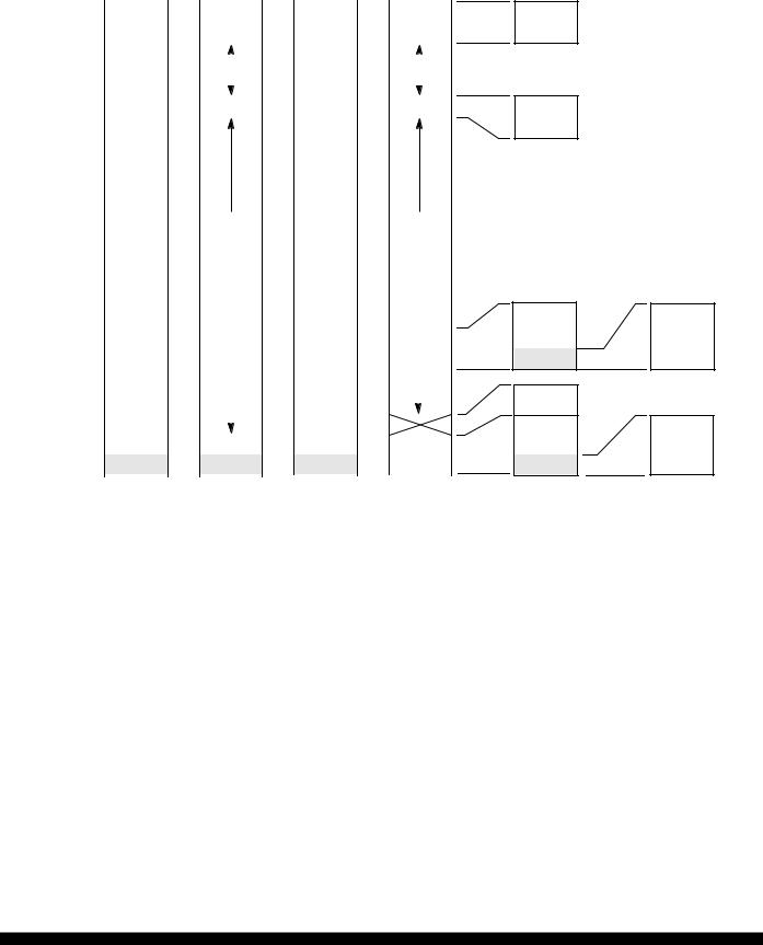
4.2 Memory Maps
$0000 — |
|
— |
|
|
— |
|
— |
|
|
|
|
|
|
|
|
||||
$03FF — |
|
— |
|
|
— |
|
— |
|
|
|
|
|
|
|
|
||||
|
|
|
|
|
|
|
|
|
|
|
|
|
|
|
|
|
|
|
|
|
|
|
EXTERNAL |
|
|
|
EXTERNAL |
||
$1000 — |
|
— |
|
|
— |
|
— |
|
|
|
|
|
|
|
|
||||
|
|
|
|
|
|
||||
$105F — |
|
— |
|
|
— |
|
— |
|
|
|
|
|
|
|
|
||||
EXTERNAL |
EXTERNAL |
$BF00 — |
— |
|
— |
|
— |
|
||||
|
||||||||||
$BFFF — |
— |
|
— |
|
— |
|
|
|||
|
|
|
|
|||||||
|
|
|
||||||||
$FE00 — |
|
|
|
|
|
|
|
|
|
|
|
|
|
|
|
|
|
|
|
|
|
|
|
|
|
|
|
|
|
|
|
|
|
|
|
|
|
|
|
|
|
|
|
|
|
|
|
|
|
|
|
|
|
|
$FFC0 — |
— |
— |
|
|
— |
|||||
$FFFF — |
|
— |
|
— |
|
|
— |
|
||
SINGLE |
EXPANDED |
|
|
SPECIAL |
||||||
|
|
|
|
SPECIAL |
|
|||||
|
CHIP |
|
|
|
|
|
BOOTSTRAP |
|
TEST |
|
|
MODA = 0 |
|
MODA = 1 |
|
|
MODA = 0 |
|
MODA = 1 |
||
|
MODB = 1 |
|
MODB = 1 |
|
|
MODB = 0 |
|
MODB = 0 |
||
NOTES:
x000
1024 BYTES RAM1
x3FF
y000
96-BYTE REGISTER FILE2
y05F
$BFC0
256 BYTES BOOTSTRAP ROM
RESERVED4
512 BYTES EEPROM5
SPECIAL
MODE
INTERRUPT
VECTORS3
$BFFF
$FFC0
NORMAL
MODE INTERRUPT VECTORS
$FFFF
1.RAM can be remapped to any 4-Kbyte boundary ($x000). “x” represents the value contained in RAM[3:0] in the INIT register.
2.The register block can be remapped to any 4-Kbyte boundary ($y000). “y” represents the value contained in REG[3:0] in the INIT register.
3.Special test mode vectors are externally addressed.
4.In special test mode the address locations $zD00—$zDFF are not externally addressable. “z” represents the value of bits EE[3:0] in the CONFIG register.
5.EEPROM can be remapped to any 4-Kbyte boundary ($z000). “z” represents the value contained in EE[3:0] in the CONFIG register.
Figure 7 MC68HC11F1 Memory Map
MC68HC11F1/FC0 |
MOTOROLA |
MC68HC11FTS/D |
19 |
$0000 — |
|
— |
|
|
— |
|
— |
|
|
|
|
|
|
|
|
||
|
|
|
|
|
|
|
|
|
|
|
|
||||||
$03FF — |
|
— |
|
|
— |
|
— |
|
|
|
|
|
|
|
|
||
|
|
|
|
|
|
|
|
|
|
|
|
||||||
|
|
|
|
|
|
|
|
|
|
|
|
|
|
|
|
||
|
|
|
|
|
|
|
|
|
|
|
|
|
|
|
|
|
|
|
|
|
EXTERNAL |
|
|
|
|
|
EXTERNAL |
|
|
|
|
|
|
||
$1000 — |
|
— |
|
|
— |
|
— |
|
|
|
|
|
|
|
|
||
|
|
|
|
|
|
|
|
|
|
|
|
||||||
|
|
|
|
|
|
|
|
|
|
|
|
||||||
$105F — |
|
— |
|
|
— |
|
— |
|
|
|
|
|
|
|
|
||
|
|
|
|
|
|
|
|
|
|
|
|
||||||
|
|
|
|
|
|
|
|
|
|
|
|
|
|
|
|
||
|
|
|
|
|
|
|
|
|
|
|
|
|
|
|
|
|
|
|
|
|
|
|
|
|
|
|
|
|
|
|
|
|
|
|
|
|
|
|
EXTERNAL |
|
|
|
|
|
EXTERNAL |
|
|
|
|
|
|
||
|
|
|
|
|
|
|
|
|
|
|
|
|
|
|
|
|
|
|
|
|
|
|
|
|
|
|
|
|
|
|
|
|
|
|
|
$BF00 — |
|
— |
|
|
— |
|
|
— |
|
|
|
|
|
|
|
256 BYTES |
|
|
|
|
|
|
|
|
|
|
|
|
|
BOOTSTRAP |
|||||
|
|
|
|
|
|
|
|
||||||||||
|
|
|
|
|
|
|
|
|
|
|
|
|
|
|
|
|
ROM |
$BFFF — |
|
— |
|
|
— |
|
|
— |
|
|
|
|
|
|
|
|
|
|
|
|
|
|
|
|
|
|
|
|
|
|
|
||||
|
|
|
|
|
|
|
|
|
|
|
|||||||
$FE00 — |
|
|
|
|
|
|
|
|
|
|
|
|
|
|
|
|
|
$FFC0 — |
|
— |
|
|
— |
|
— |
|
|
|
|
|
|
|
|
||
|
|
|
|
|
|
|
|
|
|
|
|
||||||
$FFFF — |
|
— |
|
|
— |
|
— |
|
|
|
|
|
|
|
|
||
|
|
|
|
|
|
|
|
|
|
|
|
||||||
SINGLE |
EXPANDED |
SPECIAL |
SPECIAL |
CHIP |
|
BOOTSTRAP |
TEST |
MODA = 0 |
MODA = 1 |
MODA = 0 |
MODA = 1 |
MODB = 1 |
MODB = 1 |
MODB = 0 |
MODB = 0 |
NOTES:
1024 BYTES RAM1
96-BYTE REGISTER FILE2
$BFC0
SPECIAL
MODE
INTERRUPT
VECTORS
$BFFF
$FFC0
NORMAL
MODE
INTERRUPT
VECTORS
$FFFF
1.RAM can be remapped to any 1-Kbyte boundary, depending on the value contained in the RAM field in the INIT register.
2.The register block can be remapped to $0000, $2000, or $3000, depending on the value contained in REG[1:0] in the INIT register.
Figure 8 MC68HC11FC0 Memory Map
4.3 System Initialization Registers |
|
|
|
|
|
|
|
|||
HPRIO — Highest Priority Interrupt and Miscellaneous |
|
|
|
$x03C |
|
|||||
|
Bit 7 |
6 |
5 |
4 |
3 |
2 |
1 |
Bit 0 |
|
|
|
|
|
|
|
|
|
|
|
|
|
|
RBOOT |
SMOD |
MDA |
IRV |
PSEL3 |
PSEL2 |
PSEL1 |
PSEL0 |
|
|
|
|
|
|
|
|
|
|
|
|
|
RESET: |
0 |
0 |
0 |
0 |
0 |
1 |
0 |
1 |
Single-Chip |
|
|
0 |
0 |
1 |
0 |
0 |
1 |
0 |
1 |
Expanded |
|
|
1 |
1 |
0 |
1 |
0 |
1 |
0 |
1 |
Bootstrap |
|
|
|
|
|
|
|
|
|
|
|
|
|
0 |
1 |
1 |
1 |
0 |
1 |
0 |
1 |
Special Test |
|
|
|
|
|
|
|
|
|
|
|
|
|
|
|
|
|
|
|
|
|
|
|
|
|
|
|
|
|
|
|
|
|
|
MOTOROLA |
MC68HC11F1/FC0 |
20 |
MC68HC11FTS/D |
RBOOT — Read Bootstrap ROM
RBOOT is valid only when SMOD is set to one (special bootstrap or special test mode). RBOOT can only be written in special modes but can be read anytime.
0 = Boot loader ROM disabled and not in memory map
1 = Boot loader ROM enabled and in memory map at $BF00–$BFFF
SMOD and MDA — Special Mode Select and Mode Select A
The initial value of SMOD is the inverse of the logic level present on the MODB pin at the rising edge of reset. The initial value of MDA equals the logic level present on the MODA pin at the rising edge of reset. These two bits can be read at any time. They can be written at any time in special modes. Neither bit can be written in normal modes. SMOD cannot be set once it has been cleared. Refer to Table 8.
Table 8 Hardware Mode Select Summary
Input Pins |
Mode Description |
Control Bits in HPRIO (Latched at Reset) |
||||
|
|
|
|
|
||
MODB |
MODA |
RBOOT |
SMOD |
MDA |
||
|
||||||
|
|
|
|
|
|
|
1 |
0 |
Single Chip |
0 |
0 |
0 |
|
|
|
|
|
|
|
|
1 |
1 |
Expanded |
0 |
0 |
1 |
|
|
|
|
|
|
|
|
0 |
0 |
Special Bootstrap |
1 |
1 |
0 |
|
|
|
|
|
|
|
|
0 |
1 |
Special Test |
0 |
1 |
1 |
|
|
|
|
|
|
|
|
IRV — Internal Read Visibility
This bit can be read at any time. It can be written at any time in special modes, but only once in normal modes. In single-chip and bootstrap modes, IRV has no meaning or effect.
0 = Internal reads not visible
1 = Data from internal reads is driven on the external data bus
PSEL[3:0] — See 5.2 Reset and Interrupt Registers, page 27.
INIT — RAM and I/O Mapping (MC68HC11FC0 only) |
|
|
|
|
$x03D |
|||||
|
Bit 7 |
6 |
5 |
4 |
|
3 |
2 |
1 |
Bit 0 |
|
|
|
|
|
|
|
|
|
|
|
|
|
RAM5 |
RAM4 |
RAM3 |
RAM2 |
|
RAM1 |
RAM0 |
REG1 |
REG0 |
|
|
|
|
|
|
|
|
|
|
|
|
RESET: |
0 |
0 |
0 |
0 |
|
0 |
0 |
0 |
1 |
|
The INIT register can be written only once in first 64 cycles out of reset in normal modes, or at any time in special modes.
NOTE
The register diagram above applies to the MC68HC11FC0 only. A diagram and bit descriptions of the INIT register in the MC68HC11F1 are provided elsewhere in this section.
RAM[5:0] — Internal RAM Map Position
These bits determine the upper six bits of the RAM address and allow mapping of the RAM to any oneKbyte boundary.
REG[1:0] — Register Block Map Position
These bits determine the location of the register block, as shown in Table 9.
Table 9 Register Block Location
|
REG[1:0] |
Register Block Address |
|
|
|
|
|
|
0 0 |
$0000 – $005F |
|
|
|
|
|
|
0 1 |
$1000 – $105F |
|
|
|
|
|
|
1 0 |
$2000 – $205F |
|
|
|
|
|
|
1 1 |
$3000 – $305F |
|
|
|
|
|
|
|
|
|
|
|
|
|
MC68HC11F1/FC0 |
MOTOROLA |
MC68HC11FTS/D |
21 |
Loading...