


SGS Thomson Microelectronics TL071M, TL071IN, TL071ID, TL071C, TL071ACN Datasheet
...
|
TL071 |
|
TL071A - TL071B |
LOW NOISE J-FET SINGLE OPERATIONAL AMPLIFIERS
.WIDE COMMON-MODE (UP TO VCC+) AND
.DIFFERENTIAL VOLTAGE RANGE
.LOW INPUT BIAS AND OFFSET CURRENT
.LOW NOISE en = 15nV/√ Hz (typ)
.OUTPUT SHORT-CIRCUIT PROTECTION HIGH INPUT IMPEDANCE J±FET INPUT
.STAGE
.LOW HARMONIC DISTORTION : 0.01% (typ)
.INTERNAL FREQUENCY COMPENSATION
.LATCH UP FREE OPERATION
HIGH SLEW RATE : 16V/μs (typ)
DESCRIPTION
The TL071, TL071A and TL071B are high speed J±FET inputsingle operationalamplifiersincorporating well matched, high voltage J±FET and bipolar transistors in a monolithic integrated circuit.
The devicesfeaturehigh slew rates, low input biasand offset currents, and low offset voltage temperature coefficient.
PIN CONNECTIONS (top view)
1
2
3
4
N |
D |
DIP8 |
SO8 |
(Plastic Package) |
(Plastic Micropackage) |
ORDER CODES
Part Number |
Temperature |
Package |
||
Range |
N |
D |
||
|
||||
|
|
|||
TL071M/AM/BM |
±55oC, +125oC |
• |
• |
|
TL071I/AI/BI |
±40oC, +105oC |
• |
• |
|
TL071C/AC/BC |
0oC, +70oC |
• |
• |
|
Example : TL071CN |
|
|
|
|
1 - Offset Null 1
82 - Inverting input
3 - Non-inverting input
4 - VCC-
75 - Offset Null 2
6 - Output
67 - VCC+
8 - N.C.
5
December 1998 |
1/9 |
TL071 - TL071A - TL071B
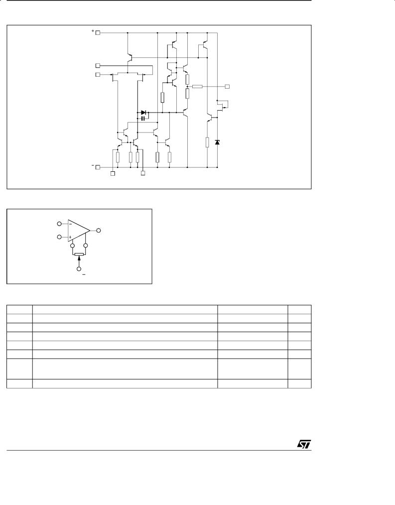
SCHEMATIC DIAGRAM
V
CC
Non-inverting
input
Inver ting input
100 Ω
200 Ω
Output
100 Ω
30k
|
|
|
|
8.2k |
1.3k |
35k |
1.3k |
3 5k |
100 Ω |
V CC |
|
|
|
|
Offset Null1 |
|
Offset Null2 |
|
|
INPUT OFFSET VOLTAGE NULL CIRCUITS
TL071
N1 N2
100k Ω
V CC
ABSOLUTE MAXIMUM RATINGS
Symbol |
Parameter |
|
Value |
Unit |
VCC |
Supply Voltage - (note 1) |
|
±18 |
V |
Vi |
Input Voltage - (note 3) |
|
±15 |
V |
Vid |
Differential Input Voltage - (note 2) |
|
±30 |
V |
Ptot |
Power Dissipation |
|
680 |
mW |
|
Output Short-circuit Duration - (note 4) |
|
Infinite |
|
Toper |
Operating Free Air Temperature Range |
TL071C,AC,BC |
0 to 70 |
oC |
|
|
TL071I,AI,BI |
±40 to 105 |
|
|
|
TL071M,AM,BM |
±55 to 125 |
|
Tstg |
Storage Temperature Range |
|
±65 to 150 |
oC |
Notes : 1. All voltage values, except differential voltage, are with respect to the zero reference level (ground) of the supply voltages where the zero reference level is the midpoint between VCC+ and VCC±.
2.Differential voltages are at the non-inverting input terminal with respect to the inverting input terminal.
3.The magnitude of the input voltage must never exceed the magnitude of the supply voltage or 15 volts, whichever is less.
4.The output may be shorted to ground or to either supply. Temperature and /or supply voltages must be limited to ensure that the dissipation rating is not exceeded.
2/9

|
|
|
|
|
TL071 - TL071A - TL071B |
|||
ELECTRICAL CHARACTERISTICS |
|
|
|
|
|
|
||
VCC = ±15V, Tamb = 25oC (unless otherwise specified) |
|
|
|
|
|
|||
|
|
|
|
TL071I,M,AC,AI, |
TL071C |
|
|
|
Symbol |
|
Parameter |
|
AM,BC,BI,BM |
|
Unit |
||
|
|
|
|
|||||
|
|
|
|
Min. Typ. Max. Min. Typ. Max. |
|
|||
Vio |
Input Offset Voltage (RS = 50Ω) |
|
|
|
|
|
mV |
|
|
Tamb = 25oC |
|
TL071 |
3 |
10 |
3 |
10 |
|
|
|
|
TL071A |
3 |
6 |
|
|
|
|
Tmin. ≤ Tamb ≤ Tmax. |
TL071B |
1 |
3 |
|
|
|
|
|
TL071 |
|
13 |
|
13 |
|
||
|
|
|
TL071A |
|
7 |
|
|
|
|
|
|
TL071B |
|
5 |
|
|
|
DVio Input Offset Voltage Drift |
|
10 |
|
10 |
|
μV/oC |
||
Iio |
Input Offset Current * |
|
|
|
|
|
|
|
|
Tamb = 25oC |
|
|
5 |
100 |
5 |
100 |
pA |
|
Tmin. ≤ Tamb |
≤ Tmax. |
|
|
4 |
|
10 |
nA |
Iib |
Input Bias Current * |
|
|
|
|
|
|
|
|
Tamb = 25oC |
|
|
20 |
200 |
20 |
200 |
pA |
|
Tmin. ≤ Tamb |
≤ Tmax. |
|
|
20 |
|
20 |
nA |
Avd |
Large Signal Voltage Gain (RL = 2kΩ, VO = ±10V) |
|
|
|
V/mV |
|
|
Tamb = 25oC |
≤ Tmax. |
50 |
200 |
25 |
200 |
|
Tmin. ≤ Tamb |
25 |
|
15 |
|
|
SVR |
Supply Voltage Rejection Ratio (RS = 50Ω) |
|
|
|
dB |
|
|
Tamb = 25oC |
≤ Tmax. |
80 |
86 |
70 |
86 |
|
Tmin. ≤ Tamb |
80 |
|
70 |
|
|
ICC |
Supply Current, no Load |
|
|
|
|
|
|
|
mA |
|
|
Tamb = 25oC |
|
|
|
|
1.4 |
2.5 |
|
1.4 |
2.5 |
|
Tmin. ≤ Tamb ≤ Tmax. |
|
|
|
|
2.5 |
|
|
2.5 |
|
Vicm |
Input Common Mode Voltage Range |
|
±11 |
+15 |
|
±11 |
+15 |
V |
||
|
|
|
|
|
|
-12 |
|
|
-12 |
|
CMR |
Common Mode Rejection Ratio (RS = 50Ω) |
|
|
|
|
|
dB |
|||
|
Tamb = 25oC |
|
|
|
80 |
86 |
|
70 |
86 |
|
|
Tmin. ≤ Tamb |
≤ Tmax. |
|
|
80 |
|
|
70 |
|
|
Ios |
Output Short-circuit Current |
|
|
|
|
|
|
|
mA |
|
|
Tamb = 25oC |
|
|
|
10 |
40 |
60 |
10 |
40 |
60 |
|
Tmin. ≤ Tamb |
≤ Tmax. |
|
|
10 |
|
60 |
10 |
|
60 |
±VOPP |
Output Voltage Swing |
|
|
|
|
|
|
|
V |
|
|
Tamb = 25oC |
|
RL = |
2kΩ |
10 |
12 |
|
10 |
12 |
|
|
|
|
RL = 10kΩ |
12 |
13.5 |
|
12 |
13.5 |
|
|
|
Tmin. ≤ Tamb ≤ Tmax. |
RL = |
2kΩ |
10 |
|
|
10 |
|
|
|
|
|
|
RL = 10kΩ |
12 |
|
|
12 |
|
|
|
SR |
Slew Rate (Vin = 10V, RL = 2kΩ, CL = 100pF, |
|
|
|
|
|
V/μs |
|||
|
Tamb = 25oC, unity gain) |
|
|
8 |
16 |
|
8 |
16 |
|
|
tr |
Rise Time (Vin = 20mV, RL = 2kΩ, CL = 100pF, |
|
|
|
|
|
μs |
|||
|
Tamb = 25oC, unity gain) |
|
|
|
0.1 |
|
|
0.1 |
|
|
KOV |
Overshoot (Vin = 20mV, RL = 2kΩ, CL = 100pF, |
|
|
|
|
|
% |
|||
|
Tamb = 25oC, unity gain) |
|
|
|
10 |
|
|
10 |
|
|
GBP |
Gain Bandwidth Product (f = 100kHz, |
|
|
|
|
|
|
MHz |
||
|
Tamb = 25oC, Vin = 10mV, RL = 2kΩ, CL = 100pF) |
2.5 |
4 |
|
2.5 |
4 |
|
|||
Ri |
Input Resistance |
|
|
|
1012 |
|
|
1012 |
Ω |
|
THD |
Total Harmonic Distortion (f = 1kHz, AV = 20dB, |
|
|
|
|
|
% |
|||
|
RL = 2kΩ, CL = 100pF, Tamb = 25oC, VO = 2VPP) |
|
0.01 |
|
|
0.01 |
|
|||
en |
Equivalent Input Noise Voltage |
|
|
|
15 |
|
|
15 |
nV |
|
(f = 1kHz, Rs = 100Ω) |
|
|
|
|
|
```√ |
||||
|
|
|
|
|
|
|
|
|
|
Hz |
m |
Phase Margin |
|
|
|
|
45 |
|
|
45 |
Degrees |
* The input bias currents are junction leakage currents which approximately double for every 10oC increase in the junction temperature.
3/9
 Loading...