


TDA8170
TV VERTICAL DEFLECTION OUTPUT CIRCUIT
.The functions incorporated are :
.POWER AMPLIFIER
.FLYBACK GENERATOR
.REFERENCE VOLTAGE THERMAL PROTECTION
DESCRIPTION
The TDA8170 is a monolithic integrated circuit in HEPTAWATTTM package. It is a high efficiency power booster for direct driving of verticalwindings of TV yokes. It is intended for use in Colour and B & W television receivers as well as in monitorsand displays.
PIN CONNECTIONS
HEPTAWATT
(Plastic Package)
ORDER CODE : TDA8170
7 |
REFERENCE VOLTAGE AND NON-INVERTING INPUT |
6 |
OUTPUT STAGE SUPPLY |
5 |
OUTPUT |
4 |
GROUND |
3 |
FLYBACK GENERATOR |
2 |
SUPPLY VOLTAGE |
1 |
INVERTING INPUT |
Tab connected to Pin 4
8170-01.EPS
BLOCK DIAGRAM
+ VS
2 |
6 |
3 |
FLYBACK
GENER ATOR
RE FER ENCE
VOLTAGE
1
PO WE R
AMPLIFIER |
5 |
7
THERMAL
P ROTE C TION
TDA8170
4
YOKE
8170-02.EPS
December 1997 |
1/7 |
TDA8170
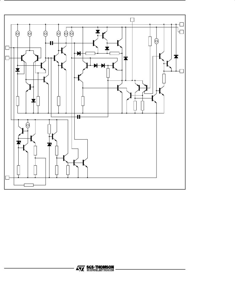
SCHEMATIC DIAGRAM
|
|
|
|
|
|
|
|
5 |
|
|
|
|
|
|
|
|
|
|
|
|
2 |
|
|
|
|
|
|
D4 |
|
|
|
6 |
|
|
|
C1 |
|
|
|
|
Q11 |
|
|
|
|
|
|
|
|
|
|
R10 |
|
|
|
|
|
|
|
|
Q10 |
Q12 |
|
||
|
|
|
|
|
|
|
|
|||
7 |
|
|
|
Q7 |
D3 |
R4 |
D5 |
R5 |
|
|
|
|
|
|
|
|
|
|
|
|
|
|
|
|
|
|
|
|
|
D8 |
Q20 |
D9 |
1 |
Q1 |
Q2 |
Q6 |
|
|
|
|
|||
|
D6 |
D7 |
|
|
|
|||||
|
|
|
|
|
|
|
Q21 |
|
||
|
|
|
Q4 |
Q8 |
|
Q9 |
|
Q13 |
|
|
|
|
|
|
|
|
|
||||
|
D1 |
|
|
|
|
|
|
|
|
3 |
|
|
|
|
|
|
|
|
R6 |
|
|
|
|
|
|
|
|
|
|
|
|
|
|
|
|
Q5 |
|
|
Q14 |
|
|
R11 |
|
|
|
|
|
|
|
|
|
Q18 |
|
|
|
|
|
|
|
|
|
|
Q15 |
|
|
|
|
|
|
|
|
|
|
|
|
|
|
Q3 |
|
|
|
|
|
Q17 |
|
|
|
|
|
|
|
|
|
|
|
Q22 |
|
|
|
|
|
|
|
|
|
|
|
|
|
|
|
|
|
|
|
|
|
Q16 |
Q19 |
|
|
R1 |
D2 |
R2 |
R3 |
|
R7 |
|
|
|
|
|
|
|
|
|
|
|||||
|
|
|
|
|
|
|
|
R8 |
R9 |
|
C2
R12
Q23
Q26
Q24
Z1
Z2
Q25
R13 R14
Q28
Q27
Q29
R15 |
R16 |
R17 |
R18 |
4
R19
8170-03.EPS
2/7

TDA8170
ABSOLUTE MAXIMUM RATINGS
Symbol |
Parameter |
|
Value |
Unit |
VS |
Supply Voltage (pin 2) |
|
35 |
V |
V5, V6 |
Flyback Peak Voltage |
|
60 |
V |
V3 |
Voltage at Pin 3 |
|
+ Vs |
|
V1, V7 |
Amplifier Input Voltage |
|
+ Vs, ± 0.5 |
V |
Io |
Output Peak Current (non repetitive, t = |
2 msec) |
2.5 |
A |
Io |
Output Peak Current at f = 50 or 60 Hz, |
t ≤ 10 μsec |
3 |
A |
Io |
Output Peak Current at f = 50 or 60 Hz, |
t > 10 μsec |
2 |
A |
I3 |
Pin 3 DC Current at V5 < V2 |
|
100 |
mA |
I3 |
Pin 3 Peak to Peak Flyback Current at f= 50 or 60 Hz, tfly ≤1.5msec |
3 |
A |
|
Ptot |
Total Power Dissipation at Tcase = 90 °C |
|
20 |
W |
Tstg, Tj |
Storage and Junction Temperature |
|
± 40, +150 |
°C |
8170-01.TBL
THERMAL DATA
Symbol |
Parameter |
|
Value |
Rth j±case |
Thermal Resistance Junction-case |
Max. |
3 |
Unit
°C/W
8170-02.TBL
ELECTRICAL CHARACTERISTICS
(refer to the test circuits, VS = 35V, Tamb = 25oC unless otherwise specified)
Symbol |
Parameter |
Test Conditions |
Min. Typ. |
Max. |
Unit |
Fig. |
|
I2 |
Pin 2 Quiescent Current |
I3 = 0, I5 = 0 |
8 |
16 |
mA |
1a |
|
I6 |
Pin 6 Quiescent Current |
I3 = 0, I5 = 0 |
16 |
36 |
mA |
1a |
|
I1 |
Amplifier Input Bias Current |
V1 = 1 V |
± 0.1 |
± 1 |
μA |
1a |
|
V7 |
Reference Voltage |
|
2.2 |
|
V |
1a |
|
V7 |
Reference Voltage Drift versus Supply Voltage |
Vs = 15 to 30 V |
1 |
2 |
mV/V |
1a |
|
VS |
|||||||
|
|
|
|
|
|
||
V3L |
Pin 3 Saturation Voltage to GND |
I3 = 20 mA |
1 |
|
V |
1c |
|
V5 |
Quiescent Output Voltage |
Vs = 35 V , Ra = 39 kΩ |
18 |
|
V |
1d |
|
|
|
Vs = 15 V , Ra = 13 kΩ |
7.5 |
|
V |
1d |
|
V5L |
Output Saturation Voltage to GND |
I5 = 1.2 A |
1 |
1.4 |
V |
1c |
|
|
|
I5 = 0.7 A |
0.7 |
1 |
V |
1c |
|
V5H |
Output Saturation Voltage to Supply |
± I5 = 1.2 A |
1.6 |
2.2 |
V |
1b |
|
|
|
± I5 = 0.7 A |
1.3 |
1.8 |
V |
1b |
|
Tj |
Junction Temperature for Thermal Shut Down |
|
140 |
|
°C |
|
8170-03.TBL
3/7
 Loading...