


TDA1675A
VERTICAL DEFLECTION CIRCUIT
.
.SYNCHRONISATION CIRCUIT
.ESD PROTECTED
PRECISION OSCILLATOR AND RAMP
.GENERATOR
POWER OUTPUT AMPLIFIER WITH HIGH
.CURRENT CAPABILITY
.FLYBACK GENERATOR
.VOLTAGE REGULATOR
.PRECISION BLANKING PULSE GENERATOR
.THERMAL SHUT DOWN PROTECTION
CRT SCREEN PROTECTION CIRCUIT WHICH BLANKS THE BEAM CURRENT IN THE EVENT OF LOSS OF VERTICAL DEFLECTION CURRENT
DESCRIPTION
The TDA1675A is a monolithic integrated circuit in 15-lead Multiwatt® package. It is a full performance and very efficient vertical deflection circuit intended for direct drive of the yoke of 110o colour TV picture tubes. It offers a wide range of applications also in portable CTVs, B&W TVs, monitors and displays.
MULTIWATT 15
(Plastic Package)
ORDER CODE : TDA1675A
PIN CONNECTIONS (top view)
15 |
FLYBACK |
14 |
SUPPLY |
13 |
BLANKING OUTPUT |
12 |
AMPLIFIER INPUT (-) |
11 |
AMPLIFIER INPUT (+) |
10 |
RAMP OUTPUT |
9 |
RAMP GENERATOR |
8 |
GROUND |
7 |
HEIGHT ADJUSTMENT |
6 |
OSCILLATOR |
5 |
SYNC. INPUT |
4 |
OSCILLATOR |
3 |
OSCILLATOR |
2 |
AMPLIFIER SUPPLY |
1 |
AMPLIFIER OUTPUT |
|
|
Tab connected to Pin 8
September 1993
1675A-01.EPS
1/11
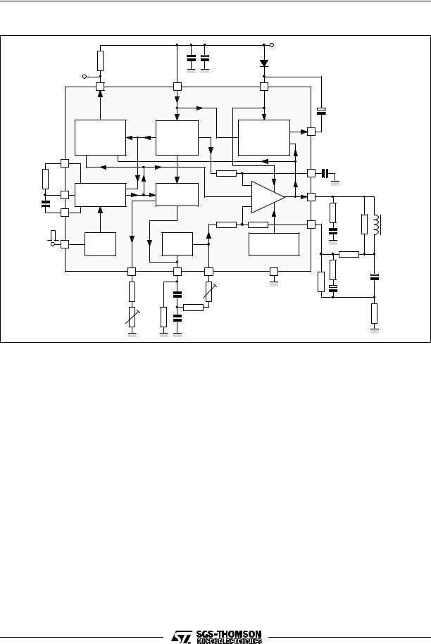
TDA1675A
BLOCK DIAGRAM
|
|
|
|
+ |
+V S |
|
|
|
|
|
|
|
|
|
|
|
|
BLANKING |
|
|
|
|
|
|
|
|
OUT |
13 |
|
14 |
|
2 |
|
|
|
|
|
|
|
|
|
|||
|
|
|
|
|
|
|
+ |
|
|
|
|
|
|
|
|
C f |
|
|
BLANK |
|
|
|
|
15 |
|
|
|
GENERATOR |
|
VOLTAGE |
|
FLYBACK |
|
|
|
|
|
|
|
|
|
|||
|
AND CRT |
|
REGULATOR |
|
GENERATOR |
|
|
|
|
PROTECTION |
|
|
|
|
|
|
|
6 |
|
|
|
|
|
|
|
|
R o |
|
|
|
|
|
11 |
|
|
|
|
|
R3 |
+ |
|
|
|
|
|
|
|
RAMP |
CLOCK |
|
|
|
|
4 |
OSCILLATOR |
|
POWER |
1 |
|
Ly |
||
|
GENERATOR |
|
||||||
C o |
|
|
PULSE |
AMP. |
|
Ry |
||
|
|
|
|
|
||||
3 |
|
|
|
|
- |
|
|
Iy |
|
|
|
R1 |
R2 |
|
|
||
|
|
|
|
12 |
Re |
YOKE |
||
|
|
|
|
|
|
|||
7 |
SYNC. |
|
BUFFER |
|
THERMAL |
|
Ra |
|
|
STAGE |
|
PROTECTION |
|
|
|||
SYNC. |
|
|
|
|
|
|
|
|
|
7 |
|
9 |
10 |
8 |
|
Rc |
+ |
|
|
|
|
|
|
Rb |
+ |
|
|
|
|
C a |
LIN |
|
|
Cc |
|
|
|
|
|
|
|
|
||
|
HEIGHT |
R d |
|
|
|
|
|
R f |
|
C b |
|
|
|
|
1675A02.EPS- |
||
|
|
|
|
|
|
|
||
|
|
|
|
|
|
|
|
ABSOLUTE MAXIMUM RATINGS
Symbol |
|
Parameter |
Value |
Unit |
|
|
|
|
|
|
|
|
|
VS |
Supply Voltage at Pin 14 |
|
|
35 |
V |
|
V1, V2 |
Flyback Peak Voltage |
|
|
65 |
V |
|
V5 |
Sync. Input Voltage |
|
|
20 |
V |
|
V11, V12 |
Power Amplifier Input Voltage |
|
VS - 10 |
V |
|
|
V13 |
Voltage at Pin 13 |
|
|
VS |
|
|
|
|
|
|
|
|
|
IO |
Output Current (non repetitive) at t = |
2ms |
3 |
A |
|
|
IO |
Output Peak Current at f = |
50Hz t > |
10μs |
2 |
A |
|
IO |
Output Peak Current at f = |
50Hz t ≤ 10 μs |
3.5 |
A |
|
|
I15 |
Pin 15 Peak-to-peak Flyback Current at f = 50Hz, tfly ≤ 1.5ms |
3 |
A |
|
||
I15 |
Pin 15 D.C. Current at V1 < V14 |
|
100 |
mA |
01.TBL |
|
Ptot |
Maximum Power Dissipation at Tcase ≤ 60oC |
30 |
W |
|||
|
|
|
|
|
|
1675A- |
Tstg, Tj |
Storage and Junction Temperature |
|
- 40, + 150 |
oC |
||
|
|
|||||
THERMAL DATA
Symbol |
Parameter |
|
Value |
Unit |
02.TBL |
|
|
|
|
|
|
RTH(j-c) |
Thermal Resistance Junction-case |
Max. |
3 |
o |
|
|
C/W |
- |
|||
RTH(j-a) |
Thermal Resistance Junction-ambient |
Max. |
40 |
oC/W |
1675A |
|
2/11

TDA1675A
DC ELECTRICAL CHARACTERISTICS (VS = 35V, Tamb = 25oC, unless otherwise specified)
Symbol |
Parameter |
|
Test conditions |
Min. |
Typ. |
Max. |
Unit |
Fig. |
|
||
|
I2 |
Pin 2 quiescent current |
I1 = 0 |
|
|
16 |
36 |
mA |
1b |
|
|
|
- I9 |
Ramp generator bias current |
V9 = 0 |
|
0.02 |
1 |
mA |
1b |
|
||
|
- I9 |
Ramp generator current |
V9 = 0 ; - I7 = 20mA |
18.5 |
20 |
21.5 |
mA |
1b |
|
||
|
ê DI 9 ê |
|
Ramp generator non linearity |
DV9 = 0 to 15V, - I7 = 20mA |
|
0.2 |
1 |
% |
1b |
|
|
|
I 9 |
|
|
||||||||
|
|
|
|
|
|
|
|
|
|
||
|
I14 |
Pin 14 quiescent current |
|
|
|
25 |
45 |
mA |
1b |
|
|
|
V1 |
Quiescent output voltage |
VS = 35V, Ra = 2.2kW, Rb = 1kW |
16.4 |
17.8 |
19.5 |
V |
1a |
|
||
|
|
|
|
VS = 15V, Ra = 390W, Rb = 1kW |
6.9 |
7.5 |
8.1 |
V |
|
|
|
|
V1L |
Output saturation voltage to ground |
I1 = 1.2A, |
|
1 |
1.4 |
V |
1c |
|
||
|
V1H |
Output saturation voltage to supply |
- I1 = 1.2A |
|
1.6 |
2.2 |
V |
1d |
|
||
|
V4 |
Oscillator virtual ground |
|
|
|
0.45 |
|
V |
1b |
|
|
|
V7 |
Regulated voltage at pin 7 |
- I7 = 20mA |
6.3 |
6.6 |
7 |
V |
1b |
|
||
|
DV 7 |
Regulated voltage drift with supply |
DVS = 15 to 35V |
|
1 |
2 |
mV |
1b |
|
||
|
DVS |
voltage |
|
V |
|
||||||
|
|
|
|
|
|
|
|
||||
|
V11 |
Amplifier input (+) reference voltage |
|
|
4.1 |
4.4 |
4.7 |
V |
1b |
03.TBL |
|
|
V13 |
Blanking output saturation voltage |
I13 = |
10 mA |
|
0.35 |
0.5 |
V |
1a |
||
|
|
1675A- |
|||||||||
|
V15 |
Pin 15 saturation voltage to ground |
I15 = |
20 mA |
|
1 |
1.5 |
V |
1a |
||
Figure 1 : DC Test Circuit. |
|
|
|
|
|
|
|
|
|||
Figure 1a |
|
|
Figure 1b |
|
|
|
|
|
|
||
|
|
|
I15 |
|
V15 |
|
VS |
|
|
|
|
|
VS |
|
|
|
|
|
|
|
|
|
|
|
|
|
|
|
|
|
|
V11 |
|
I 2 + I 1 |
|
|
I 14 |
|
|
I13 |
|
|
|
|
|
|
|
|
|
||
V13 |
|
|
|
|
A |
|
11 |
2 |
|
14 |
|
|
|
|
|
|
|
|
|
|
|||||
|
|
|
|
|
|
|
|
|
|
|||
|
|
|
|
|
|
B |
|
4 |
|
|
|
I1 |
13 |
|
2 |
14 |
15 |
|
1V |
V4 |
|
|
|
|
1 |
|
|
3 |
|
|
|
|
||||||
|
|
|
|
|
|
|
|
|
|
|
Ω |
|
|
|
|
|
|
1 |
|
|
|
|
|
|
|
7 |
|
|
|
|
|
|
|
|
|
|
22k |
|
8V |
|
|
|
|
|
|
75kΩ |
|
|
|
|
|
|
|
|
|
Ra |
|
|
|
|
|
|
||
|
|
|
|
|
|
|
5 |
|
|
|
12 |
|
|
|
|
|
|
|
|
|
|
|
|
|
|
4 |
|
|
|
|
V1 |
|
|
10 |
7 |
9 |
8 |
Ω |
|
|
|
|
|
|
47k |
||||||
1V |
|
|
|
|
12 |
|
|
|
|
|
|
|
|
|
|
|
|
|
|
|
|
|
-I 9 |
|
|
9 |
5 |
11 |
8 |
10 |
Rb |
|
|
|
|
|
|
|
|
|
V7 |
-I 7 |
|
|
|
||||||
|
|
|
|
|
|
|
|
V9 |
|
|||
-I 9 |
|
|
|
|
1675A03.EPS- |
|
|
|
|
|
1675A04.EPS- |
|
0.1µF |
|
|
|
|
|
|
|
|
|
|||
|
|
|
|
|
|
|
|
|
|
|||
|
|
|
|
|
|
|
|
|
|
|
||
Figure 1c |
|
|
|
|
|
Figure 1d |
|
|
|
|
|
|
|
VS |
|
|
|
|
|
|
VS |
|
|
|
|
|
|
2 |
14 |
|
|
|
|
2 |
14 |
|
|
|
|
|
|
|
|
+I 1 |
|
|
|
|
|
|
V1H |
4 |
|
|
|
|
1 |
|
4 |
|
|
|
1 |
|
1V |
|
|
|
|
V1L |
1V |
|
|
|
|
|
-I1 |
12 |
11 |
|
5 |
10 |
|
12 |
11 |
5 |
10 |
8 |
||
|
8 |
|
|
|||||||||
8V |
|
0.1µF |
|
1675A-05.EPS |
|
8V |
0.1µF |
|
|
1675A-06.EPS |
||
|
|
|
|
|
|
|
||||||
|
|
|
|
|
|
|
|
|
|
|
||
|
|
|
|
|
|
|
|
|
|
|
|
3/11 |
TDA1675A
AC ELECTRICAL CHARACTERISTICS |
25oC, VS = 24V, f = 50Hz, unless otherwise specified) |
|
|
|||||
(Refer to A.C. test circuit of fig. 2, Tamb = |
|
|
||||||
|
|
|
|
|
|
|
|
|
Symbol |
Parameter |
|
Test conditions |
Min. |
Typ. |
Max. |
Unit |
|
|
|
|
|
|
|
|
|
|
IS |
Supply Current |
|
IY = 2APP |
|
295 |
|
mA |
|
I5 |
Sync Input Current Required to Sync |
|
100 |
|
|
μA |
|
|
V1 |
Flyback Voltage |
|
Iy = 2App |
|
50 |
|
V |
|
V3 |
Peak-to-peak Oscillator Sawtooth |
|
I5 = 0 |
|
3.6 |
|
V |
|
|
Voltage |
|
I5 = 100μA |
|
3.4 |
|
V |
|
|
|
|
|
|
|
|
|
|
V10TH(L) |
Start Scan Level of the Input Ramp |
|
|
|
1.85 |
|
V |
|
|
|
|
|
|
|
|
|
|
tFLY |
Flyback Time |
|
Iy = 2App |
|
0.6 |
|
ms |
|
tBLANK |
Blanking Pulse Duration |
|
fo = 50Hz, Tj = 75oC |
1.33 |
1.4 |
1.47 |
ms |
|
|
|
|
fo = 60Hz, Tj = 75oC |
|
1.17 |
|
ms |
|
fo |
Free Running Frequency |
|
Ro = 7.5kΩ, Co = 330nF, Tj = 75oC |
42 |
43.5 |
46 |
Hz |
|
|
|
|
Ro = 6.2kΩ, Co = 330nF, Tj = 75oC |
|
52.5 |
|
Hz |
|
f |
Synchronization Range |
|
I5 = 100μA, Tj = 75oC |
14 |
16 |
|
Hz |
|
Tj |
Shut-down |
|
|
|
145 |
|
oC |
04.TBL- |
Junction Temperature for Thermal |
|
|
|
|
|
|||
|
|
|
|
|
|
|
|
1675A |
VON |
Peak-to-peak Output Noise |
|
|
|
|
35 |
mVPP |
|
|
|
|
|
|
||||
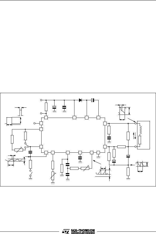
Figure 2 : AC Test Circuit
|
|
|
|
|
|
|
|
1N4001 |
220µF |
|
|
|
|
|
|
|
|
|
|
+V S |
|
1000µF |
|
|
|
|
t f Iy |
|
|
|
|
|
|
t blank |
|
|
|
|
0.1µF |
|
|
|
|
|
|
||
|
|
|
|
2.4kΩ |
|
|
|
|
|
|
|
||||
|
|
|
|
|
|
|
|
|
|
|
|
||||
|
|
|
BLANKING |
|
|
|
|
|
V1 |
|
|||||
|
|
|
|
|
|
|
|
|
GND |
|
|||||
|
|
|
OUT |
|
|
|
|
|
|
|
|
|
|
||
|
|
|
|
|
|
13 |
|
14 |
2 |
|
15 |
1/fo |
|
|
|
|
100µA |
|
|
|
|
|
|
|
|
|
|
|
|
|
|
|
|
SYNC. IN |
|
5 |
|
|
|
|
1 |
|
|
|
|
||
|
t sync. |
|
|
|
6 |
|
|
|
|
|
Ω |
|
|
YOKE |
|
|
|
|
|
|
|
|
|
|
|
|
2.2 |
|
|
||
|
|
7.5kΩ |
|
|
|
|
|
TDA 1675A |
|
|
|
|
10mH |
||
4.7kΩ |
|
|
|
|
|
|
|
|
0.22µF |
IY |
5.9Ω |
||||
|
|
|
|
|
|
|
|
|
|
270Ω |
|
|
|||
|
|
A |
S1 (Ro) |
|
|
|
|
|
|
|
2.4kΩ |
|
|
|
|
4.7kΩ |
|
B |
|
4 |
|
|
|
|
12 |
|
|
|
|
||
|
|
0.33µF |
|
|
|
|
|
|
|
|
|
||||
(FREQ.) |
|
|
Co |
|
3 |
7 |
9 |
11 |
10 |
8 |
120Ω |
|
|
|
|
tblank |
|
|
|
|
|
|
|||||||||
|
|
|
|
|
|
|
0.1µF |
|
Ω |
2200µF |
|||||
|
|
|
|
|
|
|
|
|
|
1k |
|
|
|
|
|
|
|
|
|
|
|
|
|
0.1µF |
|
|
47µF |
|
|
|
|
1/fo |
|
V3 |
15kΩ |
|
180kΩ |
|
|
|
|
|
|
R f Iy |
|||
|
|
|
56kΩ |
100kΩ |
|
|
|
|
|
||||||
|
|
|
|
560kΩ |
|
1/fo |
|
|
|
||||||
|
|
|
|
|
|
|
|
|
|
|
|
1/fo |
|||
|
|
SERVICE |
|
|
|
|
LINEARITY |
|
V10 |
R |
|
||||
|
|
|
|
|
|
|
f |
|
|||||||
|
|
SWITCH |
S2 |
|
Ω |
0.1µF |
|
|
|
||||||
|
|
|
|
|
220k |
|
GND |
|
V10thL |
|
|
07.EPS |
|||
|
|
|
|
|
|
|
|
|
|
|
|
||||
|
|
|
|
|
|
HEIGHT |
|
|
|
|
0.82Ω |
|
|
||
|
|
|
|
|
|
|
|
|
|
|
|
|
|
- |
|
|
|
|
|
|
|
|
|
|
|
|
|
|
|
1675A |
|
|
|
|
|
|
|
|
|
|
|
|
|
|
|
|
|
4/11
 Loading...