


SGS Thomson Microelectronics ST95040M6, ST95040M3TR, ST95040M3, ST95040M1TR, ST95040M1 Datasheet
...ST95040
ST95020, ST95010
4K/2K/1K Serial SPI EEPROM with Positive Clock Strobe
1 MILLION ERASE/WRITE CYCLES
40 YEARS DATA RETENTION SINGLE SUPPLY VOLTAGE
±4.5V to 5.5V for ST950x0
±2.5V to 5.5V for ST950x0W
SPI BUS COMPATIBLE SERIAL INTERFACE 2 MHz CLOCK RATE MAX
BLOCK WRITE PROTECTION STATUS REGISTER
16 BYTE PAGE MODE WRITE PROTECT
SELF-TIMED PROGRAMMING CYCLE E.S.D.PROTECTION GREATER than 4000V SUPPORTS POSITIVE CLOCK SPI MODES
DESCRIPTION
The ST950x0 is a family of Electrically Erasable Programmable Memories (EEPROM) fabricated with STMicroelectronics's High Endurance Single Polysilicon CMOS technology. Each memory is accessed by a simple SPI bus compatible serial interface. The bus signals are a serial clock input (C), a serial data input (D) and a serial data output
(Q).
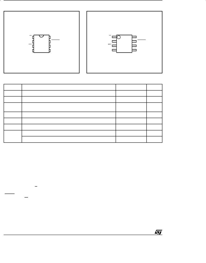
8
1
PSDIP8 (B)
0.25mm Frame
Figure 1. Logic Diagram
VCC
D
C
8
1
SO8 (M)
150mil Width
Q
Table 1. Signal Names |
S |
ST950x0 |
|
C |
Serial Clock |
W |
|
D |
Serial Data Input |
HOLD |
|
|
|
|
|
Q |
Serial Data Output |
|
|
S |
Chip Select |
|
|
W |
Write Protect |
|
VSS |
|
AI01435B |
||
|
|
|
|
HOLD |
Hold |
|
|
VCC |
Supply Voltage |
|
|
VSS |
Ground |
|
|
June 1998 |
1/18 |
ST95040, ST95020, ST95010
Figure 2A. DIP Pin Connections |
Figure 2B. SO Pin Connections |
|
ST950x0 |
|
|
ST950x0 |
|
||
S |
1 |
8 |
VCC |
S |
1 |
8 |
VCC |
Q |
2 |
7 |
HOLD |
Q |
2 |
7 |
HOLD |
W |
3 |
6 |
C |
W |
3 |
6 |
C |
VSS |
4 |
5 |
D |
VSS |
4 |
5 |
D |
|
|
AI01436B |
|
|
|
AI01437B |
|
Table 2. Absolute Maximum Ratings (1)
Symbol |
Parameter |
|
Value |
Unit |
|
TA |
Ambient Operating Temperature |
|
|
±40 to 125 |
°C |
TSTG |
Storage Temperature |
|
|
±65 to 150 |
°C |
TLEAD |
Lead Temperature, Soldering |
(SO8 package) |
40 sec |
215 |
°C |
|
|
(PSDIP8 package) |
10 sec |
260 |
|
|
|
|
|||
VO |
Output Voltage |
|
|
±0.3 to VCC +0.6 |
V |
VI |
Input Voltage with respect to Ground |
|
±0.3 to 6.5 |
V |
|
VCC |
Supply Voltage |
|
|
±0.3 to 6.5 |
V |
VESD |
Electrostatic Discharge Voltage (Human Body model) (2) |
|
4000 |
V |
|
Electrostatic Discharge Voltage (Machine model) (3) |
|
|
|
||
|
|
500 |
V |
||
Notes: 1. Except for the rating ºOperating Temperature Rangeº, stresses above those listed in the Table ºAbsolute Maximum Ratingsº may cause permanent damage to the device. These are stress ratings only and operation of the device at these or any other conditions above those indicated in the Operating sections of this specification is not i mplied. Exposure to Absolute Maximum Rating conditions for extended periods may affect device reliability. Refer also to the STMicroelectronics SURE Program and other relevant quality documents.
2.MIL-STD-883C, 3015.7 (100pF, 1500Ω)
3.EIAJ IC-121 (Condition C) (200pF, 0Ω)
DESCRIPTION (cont'd)
The device connected to the bus is selected when thechip select input (S) goes low. Communications with the chip can be interrupted with a hold input (HOLD). The write operation is disabled by a write protect input (W).
Data is clocked in during the low to high transition of clock C, data is clocked out during the high to low transition of clock C.
SIGNALS DESCRIPTION
Serial Output (Q). The output pin is used to transfer data serially out of the Memory. Data is shifted out on the falling edge of the serial clock.
Serial Input (D). The input pin is used to transfer data serially into the device. It receivesinstructions, addresses, and the data to be written. Input is latched on the rising edge of the serial clock.
2/18
ST95040, ST95020, ST95010
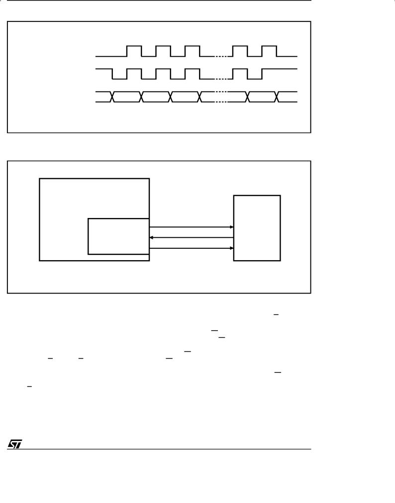
Figure 3. Data and Clock Timing
CPOL |
CPHA |
|
|
|
0 |
0 |
C |
|
|
1 |
1 |
C |
|
|
|
|
D or Q |
MSB |
LSB |
AI01438
Figure 4. Microcontroller and SPI Interface Set-up
MICROCONTROLLER
(ST6, ST7, ST9, ST10, OTHERS)
SPI Interface with (CPOL, CPHA) = ('0', '0') or ('1', '1')
SCK
C
ST95xx0
SDI
Q
SDO
D
AI01439B
Serial Clock (C). The serial clock provides the timing of the serial interface. Instructions, addresses, or data present at the input pin are latched on the rising edge of the clock input, while data on the Q pin changes after the falling edge of the clock input.
Chip Select (S). When S is high, the Memory is deselected and the Q output pin is at high impedance and, unless an internal write operation is underway the Memory will be in the standby power mode. S low enables the Memory, placing it in the active power mode. It should be noted that after
power-on, a high to low transition on S is required prior to the start of any operation.
Write Protect (W). This pin is for hardware write protection. When W is low, writes to the Memory are disabled but any other operationsstay enabled. When W is high, all writes operationsare available. W going low at any time before the last bit D0 of thedata streamwill reset the write enable latch and prevent programming. No action on W or on the write enable latch can interrupt a write cycle which has commenced.
3/18
ST95040, ST95020, ST95010
Hold (HOLD). The HOLD pin is used to pause serial communications with the Memory without resetting the serial sequence. To take the Hold condition into account, the product must be selected (S = 0). Then the Hold state is validated by a high to low transition on HOLD when C is low. To resumethe communications,HOLDis broughthigh while C is low. During the Hold condition D, Q, and C are at a high impedance state.
When the Memory is under the Hold condition, it is possibleto deselect the device. However, the serial communications will remain paused after a reselect, and the chip will be reset.
TheMemorycan bedrivenby a microcontrollerwith its SPI peripheral running in either of the two following modes: (CPOL, CPHA) = ('0', '0') or (CPOL, CPHA) = ('1', '1').
For these two modes, input data is latchedin by the low to high transition of clock C, and output data is available from the high to low transition of Clock
(C).
The differencebetween(CPOL, CPHA)= (0, 0) and (CPOL, CPHA) = (1, 1) is the stand-by polarity: C remains at '0' for (CPOL, CPHA) = (0, 0) and C remains at '1'for (CPOL, CPHA) = (1, 1) when there is no data transfer.
OPERATIONS
All instructions, addresses and data are shifted in and out of the chip MSB first. Data input (D) is sampled on the first rising edge of clock (C) after the chip select (S) goes low. Prior to any operation, a one-byte instruction code must be entered in the chip. This code is entered via the data input (D), and latched on the rising edge of the clock input
(C). To enter an instruction code, the product must have been previously selected (S = low). Table 3 shows the instruction set and format for device
Table 3. Instruction Set
operation. If an invalid instruction is sent (one not contained in Table 3), the chip is automatically deselected. For operations that read or write data in the memory array, bit 3 of the instruction is the MSB of the address, otherwise, it is a don't care.
Write Enable (WREN) and Write Disable (WRDI)
The Memory contains a write enable latch. This latch must be set prior to every WRITE or WRSR operation. The WREN instruction will set the latch and the WRDI instruction will reset the latch. The latch is reset under the following conditions:
±W pin is low
±Power on
±WRDI instruction executed
±WRSR instruction executed
±WRITE instruction executed
As soon as the WREN or WRDI instruction is received by the memory, the circuit executes the instruction and enters a wait mode until it is deselected.
Read Status Register (RDSR)
TheRDSR instructionprovidesaccessto thestatus register. The status register may be read at any time, even during a write to the memory operation. If a Read Status register reaches the 8th bit of the Status register, an additional 9th clock pulse will wrap around to read the 1st bit of the Status Register
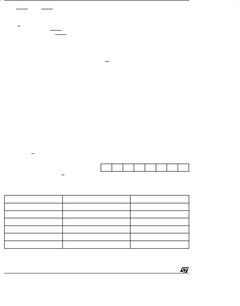
The status register format is as follows:
b7 |
|
|
b0 |
1 |
1 |
1 |
1 BP1 BP0 WEL WIP |
BP1, BP0: Read and write bits WEL, WIP: Read only bits.
b7 to b4: Read only bits.
Instruction |
Description |
Instruction Format |
|
WREN |
Set Write Enable Latch |
0000 0110 |
|
WRDI |
Reset Write Enable Latch |
0000 |
0100 |
RDSR |
Read Status Register |
0000 |
0101 |
WRSR |
Write Status Register |
0000 |
0001 |
READ |
Read Data from Memory Array |
0000 A8011 |
|
WRITE |
Write Data to Memory Array |
0000 A8010 |
|
Notes: A8 = 1, Upper page selected on ST95040.
A8 = 0, Lower page selected on ST95040.
4/18
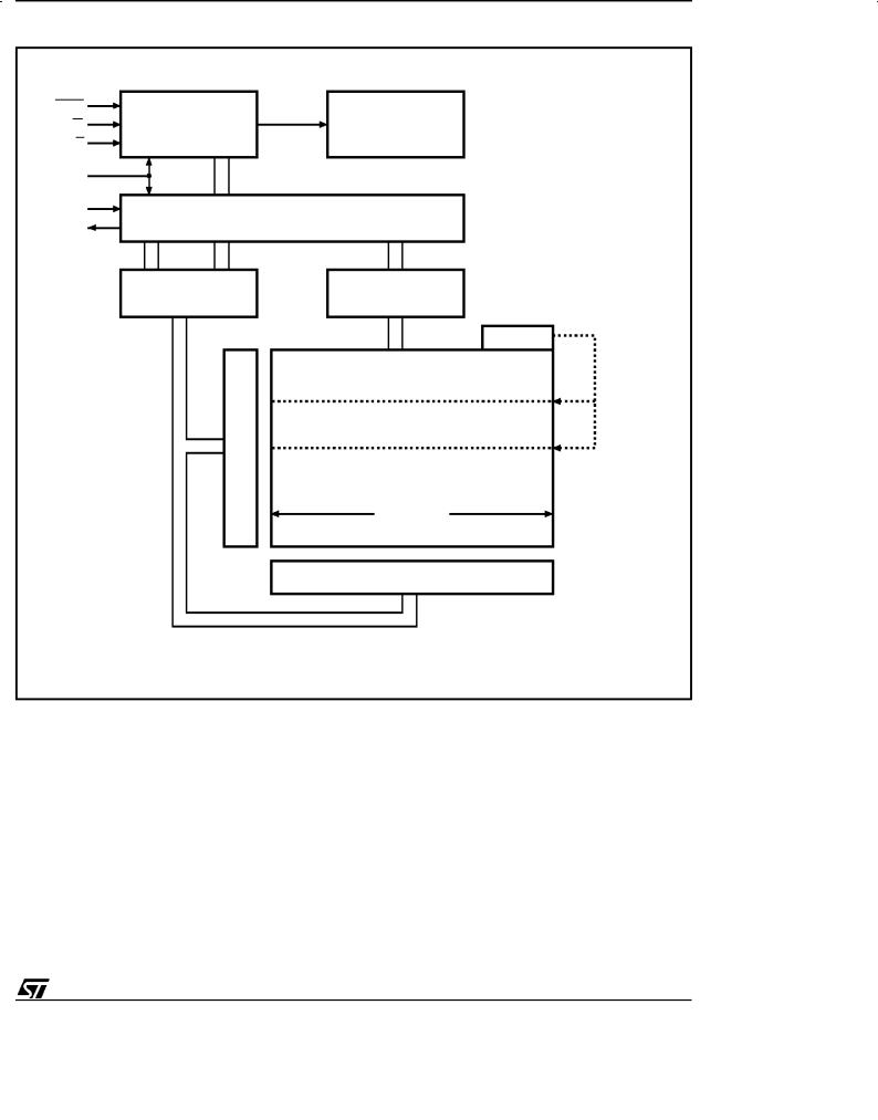
Figure 5. Block Diagram
HOLD
W Control Logic
S
C
D
I/O Shift Register
Q
Address Register
and Counter
Y Decoder
ST95040, ST95020, ST95010
High Voltage
Generator
Data
Register
Status
Block
Protect
16 Bytes
X Decoder
AI01272
During a write to the memory operation to the memory array, all bits BP1, BP0, WEL, WIP are valid and can be read. During a write to the status register, only the bits WEL and WIP are valid and can be read. The values of BP1 and BP0 read at that time correspondto the previouscontentsof the status register.
The Write-In-Process (WIP) read-only bit indicates whether the Memory is busy with a write operation.
When set to a '1' a write is in progress, when set to a '0' no write is in progress.
The Write Enable Latch (WEL) read-only bit indicates the status of the write enable latch. When set to a '1' the latch is set, when set to a '0' the latch is reset. The Block Protect (BP0 and BP1) bits indicate the extent of the protection employed. These bits are set by the user issuing the WRSR instruction. These bits are non-volatile.
5/18

ST95040, ST95020, ST95010
Figure 6. Read Operation Sequence
S |
|
|
|
|
|
|
|
|
|
|
|
|
|
|
|
|
|
|
|
|
|
|
|
0 |
1 |
2 |
3 |
4 |
5 |
6 |
7 |
8 |
9 |
10 |
11 |
12 |
13 |
14 |
15 |
16 |
17 |
18 |
19 |
20 |
21 |
22 |
23 |
C |
|
|
|
|
|
|
|
|
|
|
|
|
|
|
|
|
|
|
|
|
|
|
|
|
|
INSTRUCTION |
|
|
|
BYTE ADDRESS |
|
|
|
|
|
|
|
|
|
|
|||||||
D |
|
|
|
A8 |
|
|
|
A7 A6 A5 A4 A3 A2 A1 A0 |
|
|
|
|
|
|
|
|
|||||||
|
|
|
|
|
|
|
|
|
|
|
|
|
|
|
|
|
|
|
|
|
|
|
|
|
HIGH IMPEDANCE |
|
|
|
|
|
|
|
|
|
|
|
DATA OUT |
|
|
||||||||
|
|
|
|
|
|
|
|
|
|
|
|
|
|
|
|
1 |
|
||||||
Q |
|
|
|
|
|
|
|
|
|
|
|
|
|
|
|
7 |
6 |
5 |
4 |
3 |
2 |
0 |
|
|
|
|
|
|
|
|
|
|
|
|
|
|
|
|
|
|
|
|
|
|
|
|
|
AI01440
Notes: A8 = A7 = 0 on ST95010; A8 = 0 on ST95020; A8 is only active on ST95040.
Table 4. Write Protected Block Size
Status Register Bits |
Protected Block |
|
Array Address Protected |
|
|
|
|
|
|
|
|
BP1 |
BP0 |
|
ST95040 |
ST95020 |
ST95010 |
0 |
0 |
none |
none |
none |
none |
0 |
1 |
Upper quarter |
180h - 1FFh |
C0h - FFh |
60h - 7Fh |
1 |
0 |
Upper half |
100h - 1FFh |
80h - FFh |
40h - 7Fh |
1 |
1 |
Whole memory |
000h - 1FFh |
00h - FFh |
00h - 7Fh |
Write Status Register (WRSR)
The WRSR instruction allows the user to select the size of protected memory. The user may read the blocks but will be unable to write within the protected blocks. The blocks and respective WRSR control bits are shown in Table 4.
When the WRSR instruction and the 8 bits of the Status Register are latched-in, the internal write cycle is then triggered by the rising edge of S.
This rising edge of S must appear no later than the 16th clock cycle of the WRSR instruction of the Status Register content (it must not appear a 17th clock pulse before the rising edge of S), otherwise the internal write sequence is not performed.
Read Operation
The chip is firstselected by putting S low. The serial one byte read instruction is followed by a one byte
address (A7-A0), each bit being latched-in during the rising edge of the clock (C). Bit 3 (see Table 3) of the read instruction contains address bit A8 (most significant address bit). Then the data stored in the memory at the selected addressis shifted out on the Q output pin; each bit being shifted out during the falling edge of the clock (C). The data stored in the memory at the next address can be read in sequence by continuing to provide clock pulses. The byte address is automatically incremented to the next higher address after each byte of data is shifted out. When the highest address is reached,the address counter rolls over to 0h allowing the read cycle to be continued indefinitely. The read operation is terminated by deselecting the chip. The chip can be deselectedat anytime during data output. Any read attempt during a write cycle will be rejected and will deselect the chip.
6/18
 Loading...