


SGS Thomson Microelectronics LM311D, LM311, LM211N, LM211D, LM211 Datasheet
...LM111
LM211 - LM311
VOLTAGE COMPARATORS
.
.MAXIMUM INPUT CURRENT : 150nA
.MAXIMUM OFFSET CURRENT : 20nA
DIFFERENTIAL INPUT VOLTAGE RANGE :
.±30V
.POWER CONSUMPTION : 135mW AT ±15V
.SUPPLY VOLTAGE : +5V TO ±15V
OUTPUT CURRENT : 50mA
N |
D |
DIP8 |
SO8 |
(Plastic Package) |
(Plastic Micropackage) |
DESCRIPTION
The LM111, LM211 and LM311 are voltage comparators that have low input currents.
They are also designed to operateover a wide range of supplyvoltages : from standard ±15V operational amplifier supplies down to the single +5V supply used for IC logic.
Their outputis compatible with RTL-DTL and TTL as well as MOS circuits and can switch voltages up to +50V at output currents as high as 50mA.
PIN CONNECTIONS (top view)
ORDER CODES
Part Number |
Temperature |
Package |
||
Range |
N |
D |
||
|
||||
|
|
|||
LM111 |
±55, 125oC |
• |
• |
|
LM211 |
±40, 105oC |
• |
• |
|
LM311 |
0, 70oC |
• |
• |
|
Example : LM311D
1 |
|
8 |
1 |
- Ground |
|
|
|
2 |
- Non-inverting input |
|
|
|
3 |
- Inverting input |
2 |
+ |
7 |
|
- |
4 - VCC |
||||
|
|
|
5 |
- Balance |
3 |
- |
6 |
6 |
- Strobe/balance |
7 - Output |
||||
|
|
|
8 |
+ |
|
|
|
- VCC |
|
4 |
|
5 |
|
|
October 1997 |
1/9 |

LM111 - LM211 - LM311
SCHEMATIC DIAGRAM
|
|
|
|
S trobe/balance |
|
|
|
|
|
|
|
|
Ba lance |
|
|
||
|
300R3Ω |
300R4Ω |
|
|
|
|
|
|
|
|
|
Q6 |
R8 |
R9 |
|
||
|
|
|
|
750 |
Ω |
600Ω |
|
|
|
|
|
|
|
|
|
Q 20 |
|
|
|
|
R2 |
R5 |
Q10 |
|
|
|
|
R1 |
|
1.3kΩ |
|
|
|||
|
1.3 kΩ |
|
|
70Ω |
|
|
|
|
|
|
|
|
Q7 |
|
|
|
|
|
|
|
R6 |
R7 |
|
|
|
|
|
|
|
1.2kΩ |
1.2kΩ |
|
|
Q11 |
|
|
Q5 |
|
|
|
|
|
Q19 |
|
|
|
|
|
Q8 |
|
|
|
|
|
|
|
Q3 |
|
|
|
|
Q18 |
|
|
|
|
Q9 |
|
|
|
|
|
|
|
|
|
|
|
R 16 |
|
|
D1 D2 |
|
Q4 |
|
|
R17 |
400 |
Ω |
|
5V 5V |
|
|
|
|
60Ω |
|
|
|
|
|
|
Q21 |
|
|
|
|
Non-inverting |
Q1 |
|
|
|
|
|
|
|
input |
|
|
|
|
|
|
|
|
|
|
|
|
|
|
R15 |
|
|
|
|
|
Q23 |
|
|
450 |
Ω |
|
Inverting |
|
|
|
Q22 |
|
|
Q17 |
|
|
Q2 |
R19 |
R1 8 |
|
|
|
|
|
input |
|
|
R14 |
|
||||
|
|
|
2 50Ω |
200Ω |
|
2kΩ |
|
|
Collector output
VC C
Q12
Q13
R10
4kΩ
Q14
R11 130Ω
Q15
R12
600Ω
Q16
VC C |
R13 |
4Ω |
Emitter output or ground
ABSOLUTE MAXIMUM RATINGS
Symbol |
Parameter |
LM111 |
LM211 |
LM311 |
Unit |
VCC |
Supply Voltage |
36 |
36 |
36 |
V |
Vid |
Differential Input Voltage |
±30 |
±30 |
±30 |
V |
Vi |
Input Voltage ± (note 1) |
±15 |
±15 |
±15 |
V |
Ptot |
Power Dissipation |
|
500 |
|
mW |
Toper |
Operating Free-air Temperature Range |
±55 to +125 |
±40 to +105 |
0 to +70 |
oC |
Tstg |
Storage Temperature Range |
±65 to +150 |
±65 to +150 |
±65 to +150 |
oC |
V(1±4) |
Ground to Negative Supply Voltage |
30 |
30 |
30 |
V |
V(7±4) |
Output to Negative Supply Voltage |
50 |
50 |
40 |
V |
Output short-circuit duration : 10s |
|
LM111 : +150oC |
Voltage at strobe pin : VCC+ ±5V |
Maximum junction temperature |
LM211 : +150oC |
|
|
LM311 : +150oC |
Note : 1. This rating applies for ±15V supplies. The positive input voltage limit is 30V above the negative. The negative input voltage limit is equal to the negative supply voltage or 30V below the positive supply, whichever is less.
2/9
LM111 - LM211 - LM311
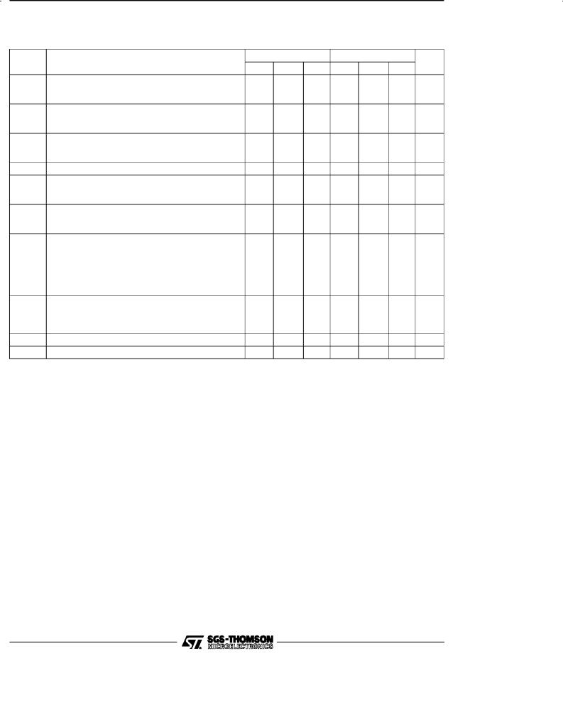
ELECTRICAL CHARACTERISTICS
VCC = ±15V, Tamb = 25oC (unless otherwise specified)
Symbol |
|
Parameter |
|
|
LM111 - LM211 |
LM311 |
|
Unit |
|||
|
|
|
Min. Typ. Max. Min. Typ. Max. |
||||||||
|
|
|
|
|
|
|
|||||
Vio |
Input Offset Voltage (RS ≤ 50kΩ) ± (note 1) |
|
|
|
|
|
mV |
||||
|
Tamb = +25oC |
|
|
|
|
0.7 |
3 |
2 |
7.5 |
|
|
|
Tmin. ≤ Tamb |
≤ Tmax. |
|
|
|
|
|
4 |
|
10 |
|
Iio |
Input Offset Current ± (note 1) |
|
|
|
|
|
|
|
nA |
||
|
Tamb = +25oC |
|
|
|
|
4 |
10 |
6 |
50 |
|
|
|
Tmin. ≤ Tamb ≤ Tmax. |
|
|
|
|
|
20 |
|
70 |
|
|
Iib |
Input Bias Current ± (note 1) |
|
|
|
|
|
|
|
|
nA |
|
|
Tamb = +25oC |
|
|
|
|
60 |
100 |
100 |
250 |
|
|
|
Tmin. ≤ Tamb |
≤ Tmax. |
|
|
|
|
|
150 |
|
300 |
|
Avd |
Large Signal Voltage Gain |
|
|
|
40 |
200 |
40 |
200 |
|
V/mV |
|
+ |
Supply Currents |
|
|
|
|
|
|
|
|
mA |
|
Positive |
|
|
|
|
|
5.1 |
6 |
5.1 |
7.5 |
|
|
ICC - |
|
|
|
|
|
|
|||||
ICC |
Negative |
|
|
|
|
|
4.1 |
5 |
4.1 |
5 |
|
Vicm |
Input Common Mode Voltage Range |
|
|
|
|
|
V |
||||
|
Tmin. ≤ Tamb |
≤ Tmax. |
|
|
|
-14.5 |
+13.8 |
+13 |
+13.8 |
+13 |
|
|
|
|
|
|
|
|
-14.7 |
-14.5 |
-14.7 |
|
|
VOL |
Low Level Output Voltage |
|
|
|
|
|
|
|
|
V |
|
|
Tamb = +25oC, IO = 50mA Vi ≤ -5mV |
|
0.75 |
1.5 |
|
|
|
||||
|
Tmin. ≤ Tamb ≤ Tmax. |
Vi ≤ -10mV |
|
|
|
0.75 |
1.5 |
|
|||
|
|
|
|
|
|
|
|
|
|
||
|
VCC+ ≥ +4.5 V, VCC- = 0 |
|
|
|
|
|
|
|
|
|
|
|
Io = 8mA |
|
Vi ≤ -6mV |
|
0.23 |
0.4 |
|
|
|
||
|
|
|
Vi ≤ -10mV |
|
|
|
0.23 |
0.4 |
|
||
IOH High Level Output Current |
|
|
|
|
|
|
|
|
|
||
|
Tamb = +25oC |
Vi |
≥ |
+ 5mV, VO = +35V |
|
0.2 |
10 |
|
|
nA |
|
|
|
|
Vi |
≥ |
+10mV, VO = +5V |
|
|
|
0.2 |
50 |
nA |
|
Tmin. ≤ Tamb ≤ Tmax. |
Vi |
≥ |
+ 5mV, VO = +35V |
|
0.1 |
0.5 |
|
|
μA |
|
Istrobe |
Strobe Current |
|
|
|
|
|
3 |
|
3 |
|
mA |
tre |
Response Time ± (note 2) |
|
|
|
|
200 |
|
200 |
|
ns |
|
Notes : 1. The offset voltage, offset current and bias current specifications apply for any supply voltage from a single +5V supply up to ±15V supplies.
The offset voltages and offset currents given are the maximum values required to drive the output down to +1V or up to +14V with a 1mA load current. Thus, these parameters define an error band and take into account the worst-case of voltage gain and input impedance.
2. The response time specified (see definitions) is for a 100mV input step with 5mV overdrive.
3/9
 Loading...