


SGS Thomson Microelectronics LM301AN, LM301AD, LM301A, LM201AN, LM201AD Datasheet
...LM101A - LM201A
LM301A
SINGLE OPERATIONAL AMPLIFIER
.
.INPUT OFFSET VOLTAGE
.INPUT BIAS CURRENT
.INPUT OFFSET CURRENT SLEW RATE AS INVERTING AMPLIFIER
LM101A LM301A LM201A
0.7mV 2mV
25nA 70nA
1.5nA 2nA 10V/μs 10V/μs
N |
D |
DIP8 |
SO8 |
(Plastic Package) |
(Plastic Micropackage) |
DESCRIPTION
The LM101A is a general-purpose operational amplifier which offers many features : supply voltages from ±5V to ±22V, low current drain, overload protectionon the inputand output,no latch-up when the common-mode range is exceeded, free from oscillations and compensationwith a single 30pFcapacitor. It has advantagesover internally compensated amplifiers in that the compensation can be tailored to theparticular application : slew rate of 10V/μs and bandwidth of 3.5MHz can be easily achieved.
PIN CONNECTIONS (top view)
ORDER CODES
Part |
Temperature |
Package |
|
Number |
Range |
N |
D |
|
|
||
LM101A |
-55oC, +125oC |
• |
• |
LM201A |
-40oC, +105oC |
• |
• |
LM301A |
0oC, +70oC |
• |
• |
Example : LM201AN
1 |
8 |
1 |
- Balance - compensation 1 |
|
2 |
- Inverting input |
|||
2 |
7 |
3 |
- Non-inverting input |
|
4 |
- VCC- |
|||
|
|
|||
3 |
6 |
5 |
- Balance |
|
6 |
- Output |
|||
|
|
|||
4 |
5 |
7 |
- VCC+ |
|
|
|
8 |
- Compensation 2 |
October 1995 |
1/11 |

LM101A - LM201A - LM301A
SCHEMATIC DIAGRAM
ABSOLUTE MAXIMUM RATINGS
Symbol |
Parameter |
|
LM101A |
LM201A |
LM301A |
Unit |
|
Vcc |
Supply Voltage |
|
|
|
±22 |
|
V |
Vid |
Differential Input Voltage |
|
|
|
±30 |
|
V |
Vi |
Input Voltage |
|
|
|
±15 |
|
V |
Ptot |
Power Dissipation |
N Suffix |
|
|
500 |
|
mW |
|
|
D Suffix |
|
|
300 |
|
|
|
Output Short-circuit Duration |
|
|
|
Infinite |
|
|
Toper |
Operating Free Air Temperature Range |
-55 |
to +125 |
-40 to +105 |
0 to +70 |
oC |
|
Tstg |
Storage Temperature Range |
|
-65 |
to +150 |
-65 to +150 |
-65 to +150 |
oC |
2/11
|
|
|
|
|
|
|
LM101A - LM201A - LM301A |
||||
ELECTRICAL CHARACTERISTICS |
|
|
|
|
|
|
|
|
|
||
LM301A |
0oC < Tamb < +70oC |
|
±5V ≤ VCC ≤ |
±20V |
|
C1 = 30pF |
|
|
|||
LM201A |
-40oC < Tamb < +105oC |
±5V ≤ VCC ≤ |
±20V |
|
C1 = 30pF |
|
|
||||
LM101A |
-55oC < Tamb < +125oC |
±5V ≤ VCC ≤ |
±20V |
|
C1 = 30pF |
|
|
||||
Symbol |
Parameter |
|
|
LM101A - LM201A |
|
LM301A |
|
Unit |
|||
|
|
Min. |
Typ. |
Max. |
Min. |
Typ. |
Max. |
||||
|
|
|
|
|
|
||||||
Vio |
Input Offset Voltage (RS ≤ 10kΩ) |
|
|
|
|
|
|
|
mV |
||
|
Tamb = +25oC |
|
|
|
|
0.7 |
2 |
|
2 |
7.5 |
|
|
Tmin. ≤ Tamb ≤ Tmax. |
|
|
|
|
3 |
|
|
10 |
|
|
DVio |
Input Offset Voltage Drift |
|
|
|
3 |
15 |
|
6 |
30 |
μV/oC |
|
|
Tmin. ≤ Tamb ≤ |
Tmax. |
|
|
|
|
|
|
|
|
|
Iib |
Input Bias Current |
|
|
|
|
|
|
|
|
nA |
|
|
Tamb = +25oC |
|
|
|
|
25 |
75 |
|
70 |
250 |
|
|
Tmin. ≤ Tamb ≤ Tmax. |
|
|
|
|
100 |
|
|
300 |
|
|
Iio |
Input Offset Current |
|
|
|
|
|
|
|
|
nA |
|
|
Tamb = +25oC |
|
|
|
|
1.5 |
10 |
|
2 |
50 |
|
|
Tmin. ≤ Tamb ≤ Tmax. |
|
|
|
|
20 |
|
|
70 |
|
|
DIio |
Input Offset Current Drift |
|
|
|
|
|
|
|
|
pA/oC |
|
|
25oC ≤ Tamb ≤ Tmax. |
|
|
|
10 |
100 |
|
10 |
300 |
|
|
|
Tmin. ≤ Tamb ≤ |
Tmax. |
|
|
|
20 |
200 |
|
20 |
600 |
|
Avd |
Large Signal Voltage Gain * |
|
|
|
|
|
|
|
|
V/mV |
|
|
(VO ≤ 10V, RL = 2kΩ) |
|
|
|
|
|
|
|
|
|
|
|
Tamb = +25oC |
|
|
|
50 |
100 |
|
25 |
100 |
|
|
|
Tmin. ≤ Tamb ≤ Tmax. |
|
|
25 |
|
|
15 |
|
|
|
|
SVR |
Supply Voltage Rejection Ratio |
|
|
|
|
|
|
|
dB |
||
|
(RS ≤ 10kΩ) |
|
|
|
|
|
|
|
|
|
|
|
Tamb = +25oC |
|
|
|
80 |
96 |
|
70 |
96 |
|
|
|
Tmin. ≤ Tamb ≤ Tmax. |
|
|
80 |
|
|
70 |
|
|
|
|
ICC |
Supply Current, no load |
|
|
|
|
|
|
|
|
mA |
|
|
Tamb = +25oC |
|
|
|
|
1.8 |
3 |
|
1.8 |
3 |
|
|
Tmin. ≤ Tamb ≤ Tmax. |
|
|
|
|
3 |
|
|
3 |
|
|
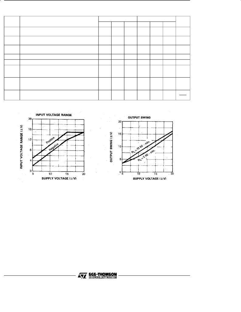
Vicm |
Input Common Mode Voltage Range |
|
|
|
|
|
|
|
V |
||
|
(VCC = ±20V) |
|
|
|
|
|
|
|
|
|
|
|
Tamb = +25oC |
|
|
|
±15 |
|
|
±15 |
|
|
|
|
Tmin. ≤ Tamb ≤ Tmax. |
|
|
±15 |
|
|
±15 |
|
|
|
|
CMR |
Common-mode Rejection Ratio |
|
|
|
|
|
|
|
dB |
||
|
(RS ≤ 10kΩ) |
|
|
|
|
|
|
|
|
|
|
|
Tamb = +25oC |
|
|
|
80 |
96 |
|
70 |
96 |
|
|
|
Tmin. ≤ Tamb ≤ Tmax. |
|
|
80 |
|
|
70 |
|
|
|
|
IOS |
Output Short-circuit Current * |
|
|
|
|
|
|
|
|
mA |
|
|
Tamb = +25oC |
|
|
|
10 |
30 |
50 |
10 |
30 |
50 |
|
±VOPP |
Output Voltage Swing * |
|
|
|
|
|
|
|
|
V |
|
|
Tamb = +25oC |
|
RL = 10kΩ |
12 |
14 |
|
12 |
14 |
|
|
|
|
|
|
RL = 2kΩ |
10 |
13 |
|
10 |
13 |
|
|
|
|
Tmin. ≤ Tamb ≤ Tmax. |
RL = 10kΩ |
12 |
|
|
12 |
|
|
|
||
|
|
|
RL = 2kΩ |
10 |
|
|
10 |
|
|
|
|
3/11
LM101A - LM201A - LM301A
ELECTRICAL CHARACTERISTICS (continued)
Symbol |
Parameter |
LM101A - LM201A |
|
LM301A |
Unit |
||
Min. |
Typ. Max. Min. Typ. Max. |
||||||
|
|
|
|||||
SR |
Slew Rate (Vi = ±10V, RL =2kΩ, CL= 100pF, |
|
|
|
|
V/μs |
|
|
Tamb = 25oC, unity gain) - (note 1) * |
0.25 |
0.5 |
0.25 |
0.5 |
|
|
tr |
Rise Time (Vi = ±20μV, RL = 2kΩ, CL = 100pF, |
|
|
|
|
μs |
|
|
Tamb = 25oC, unity gain) * |
|
0.3 |
|
0.3 |
|
|
KOV |
Overshoot (Vi = 20mV, RL = 2kΩ, CL = 100pF, |
|
|
|
|
% |
|
|
Tamb = 25oC, unity gain) |
|
5 |
|
5 |
|
|
Zi |
Input Impedance * |
1.5 |
4 |
1.5 |
4 |
MΩ |
|
Ro |
Output Resistance * |
|
75 |
|
75 |
Ω |
|
GBP |
Gain Bandwidth Product * |
|
|
|
|
MHz |
|
|
(Vi = 10mV, RL = 2kΩ, CL= 100pF, f = 100kHz, |
0.5 |
1 |
0.5 |
1 |
|
|
|
Tamb = 25oC) |
|
|
|
|
|
|
THD |
Total Harmonic Distortion |
|
|
|
|
% |
|
|
(f = 1kHz, AV = 20dB, RL =2kΩ, VO = 2VPP, |
|
0.015 |
|
0.015 |
|
|
|
CL = 100pF, Tamb = 25oC) |
|
|
|
|
|
|
en |
Equivalent Input Noise Voltage |
|
25 |
|
25 |
nV |
|
|
(f = 1kHz, Rs = 100Ω) |
|
|
|
|
```√ Hz |
|
Notes : 1. May be i mproved up to 10V /μs in invert ing ampli fier configuration * = > VCC = ±15V Tamb = +25oC (unl ess ot herwise specified)
4/11
 Loading...